Approximate MRAM: High-performance and Power-efficient Computing with MRAM Chips for Error-tolerant Applications
Abstract
Approximate computing (AC) leverages the inherent error resilience and is used in many big-data applications from various domains such as multimedia, computer vision, signal processing, and machine learning to improve systems performance and power consumption. Like many other approximate circuits and algorithms, the memory subsystem can also be used to enhance performance and save power significantly. This paper proposes an efficient and effective systematic methodology to construct an approximate non-volatile magneto-resistive RAM (MRAM) framework using consumer-off-the-shelf (COTS) MRAM chips. In the proposed scheme, an extensive experimental characterization of memory errors is performed by manipulating the write latency of MRAM chips which exploits the inherent (intrinsic/extrinsic process variation) stochastic switching behavior of magnetic tunnel junctions (MTJs). The experimental results, involving error-resilient image compression and machine learning applications, reveal that the proposed AC framework provides a significant performance improvement and demonstrates a reduction in MRAM write energy of on average with negligible or no loss in output quality.
Index Terms:
Approximate Computing, MRAM, Cache Write Policy, Low Power Design, Approximate MRAM.1 Introduction
The amount of unstructured data processing from numerous modern computing platforms, from mobile to the cloud, is increasing rapidly. Therefore, we need an efficient framework to mitigate the gap between processor and memory systems and accomplish the computational and storage demands of the current computing system, even in advanced multi-core processors. In addition, memories consume a significant power and chip area, becoming the computing system’s main bottleneck. Moreover, continual scaling down in technology nodes introduces additional challenges to the conventional memory chips, such as increased leakage power, substantial process variation, high sensitivity with different operating conditions, etc. Existing mainstream volatile memory chips, i.e., static RAM (SRAM) and dynamic RAM (DRAM), suffer from density, scalability, memory persistency, and leakage issues. Besides, current non-volatile memory (NVM) chips (e.g., Flash) suffer from endurance and performance problems. These limitations make existing memory chips incompetent for delivering ever-increasing demands of power-efficient, high-performance systems with the growing number of cores and data volume [1].
Fortunately, data-intensive emerging applications in graphics/multimedia, data-driven inference, computer vision, data mining, and machine learning exhibit intrinsic error resilience properties. Therefore, those applications can produce outputs with acceptable quality in the presence of data or computation approximations [2]. Approximate computing (AC) attains performance and power improvement by orders of magnitude using software, architecture, and circuit-level techniques [3, 2]. Therefore, AC is attracting significant interest in implementing approximate memories by relaxing the strict constraints on data integrity in a controlled manner, and as a result, saves significant power consumption as well as improves performance notably.
MRAM chip has significant potential to turn into a dominant universal memory (cache or main memory) technology due to its attractive characteristics, such as non-volatility, scalability, high speed and fast access latencies, large endurance, ultralow-power operation, CMOS compatibility, high density, reliability, near-zero leakage, almost zero static power, thermal robustness, radiation hardness, etc. [4]. These advantageous features make MRAM suitable to integrate into most of the systems. Therefore, MRAM can be an excellent candidate for energy-efficient on-chip memory. However, the higher write current for a sufficiently long duration is required for proper magnetic switching during the write operation, limiting the overall energy efficiency. Several promising research has been performed on the circuit, device, and architecture levels to improve the energy efficiency of MRAM [5, 6, 7, 8]. This paper proposes a new dimension of MRAM-based approximate approach to attain significant performance and power gain by introducing a small number of errors that most error-resilient applications can endure.
The major challenge in AC is managing the approximations to trade-off between the application quality and device performance (i.e., energy, speed, etc.). Most AC-based prior works are focused on processing or logic circuits and can be categorized based on the targeted memory hierarchy level [9, 10, 11, 12, 13, 14]. These works focus on (i) secondary storage and main memory [9, 10], (ii) application-specific memory designs [11, 12], and (iii) CMOS memory-based approximate cache architecture [13, 14]. However, the existing MRAM-based AC framework is mostly simulation-based requires extension in either new instruction set architecture (ISA) or enhancement in cache replacement policies along with device-circuit-architecture remodeling [12, 8]. Hence, these MRAM-based AC frameworks can not be easily integrated into the existing computing system due to the above-mentioned strict requirements. The previous contributions inspirit the need for real memory implementation and build the foundation of the proposed MRAM-based AC framework using commercial-off-the-shelf (COTS) MRAM chips, which require minimal or no additional hardware, is robust against operating conditions. To this end, we propose a system-level MRAM-based experimental AC framework that works at the reduced write latency of COTS MRAM chips to improve computation speed significantly and energy efficiency with the cost of small write accuracy.
This paper presents a new approach to constructing an approximate MRAM framework. We also introduce a data allocation scheme based on the cell characterization algorithm for the proposed framework. The core idea is that at sub-optimal write latency, MRAM addresses can be split into accurate and approximate addresses through extensive error characterization of COTS toggle MRAM chips. The correlation between the obtained errors and the application-level output quality guides the proper allocation of application data to MRAM addresses. The more straightforward implementation of the proposed mechanism results in a better speed-power-quality trade-off. In summary, the key contributions of this work are as follows.
-
•
We reduce the write enable () time from the manufacturer’s recommended value during the write operation to introduce errors. We extensively characterize these errors using COTS Everspin toggle MRAM chips [15] to improve write power efficiency by exploiting the applications’ error-resilient nature. The characterization results are used to derive key insights about memory errors — for example, toggling from “1” “0” and “0” “1” are mutually exclusive.
-
•
Insights obtained from the characterization guide us in constructing a systematic data allocation scheme based on the application requirements to store critical and approximate data considering the occurrence and properties of MRAM errors by writing different intuitive and non-intuitive input data patterns. Subsequently, approximate data can be stored in the approximate addresses, whereas critical data must be allocated in entirely accurate memory addresses.
-
•
We analyze a detailed trade-off between the application-level output accuracy and system-level performance/power gains by determining optimal write latency.
-
•
We implement our AC framework using our custom memory controller implemented on Xilinx Artix 7 (XC7A35T-1C) FPGA to manipulate different timing latency of a couple of emerging memories [16]. Our experimental results show a significant improvement in the speed-power-quality trade-off, an average write speed-up of and power savings of with minimal or no loss in application quality.
The rest of the paper is organized as follows. Sect. 2 provides an overview of related prior work. Sect. 3 briefly overviews the organization and operating principle of MRAM chips and related preliminaries of cache writing policies. Sect. 4 presents the proposed AC framework, including the cell characterization algorithm. Sect. 5 explains the experimental setup and exhibits obtained results. Sect. 6 discusses the characterization and memory overhead required to store the erroneous memory addresses along with the proposed scheme’s applicability to next-generation MRAMs. Finally, Sect. 7 concludes the article.
2 Related Work
This work correlates two distinct research areas – emerging MRAM memories with approximate computing. Previous simulation-based MRAM-related work focuses on addressing spintronic memories’ high write energy while preserving accurate read/write operations to achieve energy-efficient on-chip memories using the circuit, architectural, and device-level techniques [17, 18, 19, 20, 21, 22, 6]. In [17], using the bit-line voltage clamping technique, MRAM write-current asymmetry is mitigated at the circuit level to achieve the goal. Besides, in [18], a co-design methodology focusing on the bit-cell access transistor and the supply voltage is proposed to improve energy efficiency. Moreover, the MRAM cell’s actual switching time detection technique is proposed to cease the unnecessary current flow immediately after a complete write [21]. Significant write energy reduction is achieved for such techniques; however, the overall write latency remains the same. On the other hand, at the architectural level, in [19, 20], the proposed hybrid CMOS-spintronic cache can selectively direct the write-intensive memory blocks to the CMOS portion while keeping the remaining blocks in the spintronic part to address the write-inefficiency of the spintronic memories. Besides, redundant memory writes are eliminated by comparing the previously stored data before the write operation [21] or tracking dirty data at a finer granularity [22]. In addition, in [23], significant write margin reduction is achieved by exploiting incomplete write operations, and the incomplete bits are processed through robust Error Correction Codes (ECCs) at the cost of large decoding latencies (impairing the memory read latency). Furthermore, at the device level, in [6, 24], volatile spintronic memory is proposed by relaxing the non-volatility property (data-retention-time) or the current to overcome high write latency and energy issues of STT-MRAMs at the cost of higher write errors. However, those proposed techniques require an additional data refresh scheme to avoid further retention errors. Besides, in [25], the thermal stability factor [26], which defines the stability of the free layer’s magnetic orientation against thermal noise, is reduced to address extreme write margin at the cost of a higher overall failure rate and retention time.
In addition to the above techniques, a few previous AC-based frameworks explore different layers of abstraction spanning software or circuits, architectures, and algorithms to reduce the consumed energy in processing cores/accelerators. Introducing errors in the memory subsystem is an effective way of exploiting the applications’ intrinsic error resilience. However, we concentrate on prior works related to approximate memories since that aligns with this work. Prior works on approximate DRAMs [9, 10] relax their refresh rate to inject retention errors in the saved or read data contents in exchange for refresh power savings. On the other hand, [27] proposes approximate multilevel PCMs that can (i) reduce the number of programming pulses to inject write errors in exchange for energy savings and (ii) perform partial error correction on the most significant bits of the worn-out blocks. However, spintronic memories require exploring new technique due to the in-applicability of the mentioned approximation mechanisms. Moreover, [12, 28] proposed simulation-based enhanced architectural and software approximate design models by accessing cells in the memory arrays with different current levels depending on application requirements at the cost of higher read/write error rates. The proposed technique can (i) specify acceptable error probabilities for groups of bits within the word by controlling the quality of the read/write operations (ii) regulate (by software) the numerical significance of errors incurred during approximate load/store operations. However, this work entirely ignores the process variation effect. The process variation in spintronic memories affects both the MTJ cell and CMOS transistor parameters, which, in turn, impacts the parameters associated with read/write operations such as switching current, thermal stability factor, transistor’s output current, etc. Consequently, the output accuracy at the architecture level will vary considerably with process variation due to these different and lower read/write access current levels. In [8], another simulation-based new approximate spintronic on-chip memory design is proposed by relaxing both device and circuit parameters of spintronic memories by increasing various failure rates such as read disturb, retention and read decision failures, along with write errors to improve energy consumption and performance.
In contrast, our work renders a speed-power-quality trade-off through an actual memory implementation by employing COTS MRAM chips that (i) require minimal or no additional hardware, (ii) are robust against diverse operating conditions, and (iii) achieve power and performance improvements over and beyond the previous techniques, which is the key uniqueness of the proposed work.
3 Background
3.1 MRAM: Preliminaries
The core element of toggle MRAM is the magnetic tunnel junction (MTJ) that uses the Savtchenko switching [29] property to store both data states (high and low). The 1T-1MTJ MRAM bit cell comprises two ferromagnetic layers separated by a thin dielectric tunnel oxide ( or ) layer (Fig. 1(a)). One layer’s magnetic orientation is permanently fixed, commonly referred to as the reference (or fixed) magnetic layer (RML). In contrast, the other layer’s magnetization can freely be oriented depending on the magnetic field, known as the free magnetic layer (FML). The substantially higher magnetic anisotropy of RML compared to FML ascertains the stable magnetization direction of FML during memory read/write operation. The resistance states determine the bit that will be stored in the memory array. When both the FML and RML are aligned in the same direction, the MTJ produces low electrical resistance. On the other hand, when their magnetic field orientation is opposite, the resistance becomes extremely large; hence, almost no current or weak current flows through the barrier layer. Therefore, the MTJ exhibits high electrical resistance.
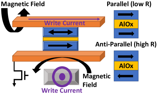
Writing a bit in the magnetic field-driven toggle MRAM array requires passing a high write current () for changing FML’s magnetic orientation [29]. The applied to the write lines, placed on top and bottom of the MTJ devices (see Fig. 1(a)), creates an auxiliary magnetic field that changes the FML direction in the required position. Contrastingly, the RML’s direction is strongly coupled with an anti-ferromagnet [29]. During the write operation, the memory circuit performs a pre-read operation to determine the state of the target bit and execute a toggle pulse (if required) to change the state of the bit if the desired state is not the same as the targeted state. Consequently, it reduces the overall power consumption and improves power efficiency. However, this increases the total write cycle time (including an additional read operation).
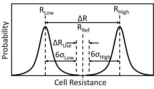
A small bias voltage (far below the device’s breakdown voltage) is applied across the MRAM cell during the read cycle. Depending on parallel () or anti-parallel () magnetic orientation, a current sensing circuitry that is attached with the MRAM cell experiences different amounts of current and latches the appropriate logic (“0” or “1”) compared with the reference resistance () shown in Fig. 1(b). Note that the width of resistance distribution varies from cell to cell because of manufacturing process variations. Besides, the quality, size, and level of in-homogeneity of the MTJ tunnel barrier significantly impact larger relative bit-to-bit resistance variation [29].
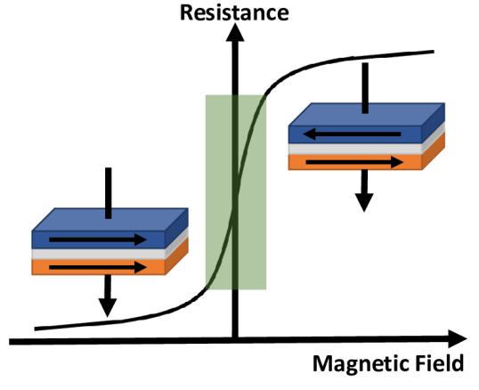
However, from Fig. 1(c), we observe that the change in resistance due to the change in the induced magnetic field is steep in a certain region (the green region on Fig. 1(c)). In this region, a slight change in the induced magnetic field may cause a drastic change in resistance states and alter the decision of the read circuitry. Therefore, manufacturers define timing parameters for all commercial memory chips for reliable write/read operation against a wide range of operating conditions. For toggle MRAM, the write operation is governed by three different control signals: write enable (), chip enable (), and upper/lower byte enable (/) signals [15]. A simplified version of the write enable () controlled write operation of the MRAM chip is shown in Fig. 2.
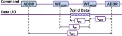
Here,
= write cycle time, i.e., the time period to complete full write operation in a particular address.
= write pulse width, i.e., the time period for which the pin is kept activated.
= write recovery time, i.e., the time to complete the write operation after the pin is deactivated.
= valid data to end of write, i.e., the time for which the valid data need to be available in the data I/O before the pin is deactivated.
Reducing any of these timing parameters can improve the speed and reduce power consumption but may lead to faulty operation. The write timing parameter is manipulated in this work to introduce errors during the -controlled write operation.
3.2 Read vs. Write Latency
Due to the technology limitation, the MRAM is still much slower than the most commonly used SRAM cache ( access time on MRAM vs. – access time on SRAM cache). Hence, we will keep our discussion limited by considering MRAM as the main memory in this section. However, it is worth mentioning that our proposed reducing MRAM write latency strategy will also improve the system performance, even if it is used as a cache.
In a computer system, the main memory is only accessed when there is a cache miss (read/write miss). Usually, recovering a read miss is a direct procedure; i.e., when a read miss occurs, the corresponding memory block (usually consists of multiple data words) of the main memory is copied directly to the cache. However, by taking proper caution at the software level, one can maximize the cache hit rate and hide the read access latency of the main memory. For example, the average cache miss rate in a modern computer processor is 8% for most use-cases [31]. On the other hand, handling a write miss is more complex. Usually, most of the modern processors use either of the following two policies- (i) write-through policy with the no-write allocation and (ii) write back policy with write allocation [32]. The first policy is not used in high-end processors since it requires a long time to proceed. However, both cache miss policies become more complex if some of the memory resources are shared by the multiple processor cores (e.g., L2/L3 caches and the main memory) and require a dedicated cache coherency protocol. As the write miss recovery procedure is more complex than the read miss, the write miss penalty is much higher than the read miss penalty. Moreover, the write miss penalty might become a critical bottleneck for write-intensive program performance (e.g., iterative weight updating on neural networks). Moreover, write operations consume a significant portion of total energy[8, 12]. Hence, in this work, we aim to reduce such penalties by improving the write access time of MRAMs.
Furthermore, big data applications allow data approximation to some extent, motivating us to develop an AC framework to investigate the trade-off between application-level acceptable output accuracy vs. system-level power/performance gain in the memory system.
4 MRAM Approximate Computation Framework
Random Savtchenko switching property is exploited at the reduced timing parameter in our proposed methodology to obtain data approximation at the application level. At reduced write pulse width, , of toggle MRAM (see Fig. 2), all memory cells do not receive sufficient write current and time to toggle into the intended stable state. These random variations are created in the MTJ storage element due to the process variation and the non-uniform distribution of the current pulse within the chip, which hinders performing an appropriate write operation in all memory cells. That is why the manufacturer specifies a set of timing parameters for reliable read/write operations. Hence, violation in any of these manufacturer-recommended timing parameters may cause erroneous/faulty outputs during the read/write operation. If the is insufficient, there is a high chance that FML cannot align perfectly with the RML (either the same or opposite direction) and might be settled on an intermediate position, leading to the cell resistance being halfway between and [30]. Therefore, at reduced , if the resultant cell resistance falls around the region of the resistance distribution (see Fig. 1(b)) curve, the cell will show indeterministic characteristics and generate erroneous bits.
Several steps are involved in our proposed scheme. At the reduced , MRAM chips create errors, and the total number of errors differs at different reduced values. At first, we select the most suitable reduced value. This selected aims to generate erroneous bits at a tolerable range for error-resilient applications. Second, we propose a cell selection algorithm to characterize all MRAM cells from a set of measurements by writing a specific data pattern that produces maximum error compared with other data patterns to identify the erroneous (approximate) and error-free (accurate) memory cells/addresses for the AC framework. The characterization needs to be performed only once to choose the appropriate number of MRAM cells/addresses. Finally, we collect data by writing all necessary data patterns into the entire memory to gain valuable insights about the bit errors’ frequency, significance, and nature.
4.1 Appropriate Reduced Time Selection
Appropriate reduced time selection is essential for obtaining the most favorable trade-off between application quality and speed/power improvement. Towards this end, the experimental results reveal that some of the memory cells provide erroneous outputs if the data is written at the reduced timing parameters [33]. The number of these error-prone cells varies within the write pulse activation time range t = [0 ]. The total number of erroneous bit cells is counted by changing the and writing different input data patterns at different . The main objective is to determine a suitable for which the acceptable amount of erroneous bits is achieved. In the next step, the number of erroneous cells is calculated from all achievable reduced write timing parameters. Finally, we propose an algorithm to characterize the erroneous memory cells for the AC framework using the timing parameter for which the sustainable amount of error bits is obtained.
4.2 Erroneous Address Selection
Our experimental result manifests that only a few memory cells, hence addresses are error-prone at a specific sub-optimal write latency. To locate these cells, we characterize MRAM memory cells by writing different intuitive (solid) and nonintuitive (random, checkerboard, and striped) input data patterns to the entire memory cells at the reduced write enable time, , and read back the entire memory contents with appropriate timing parameters a total of times. Larger provides better characterization results, but it increases the computation time.
To toggle magnetic direction, parallel (P) anti-parallel (AP), or vice versa, in the MRAM cell, the write current () needs to be held sufficiently long [34]. If we reduce the write time (i.e., pulse width), the cell resistance might be stuck in an intermediate value (anywhere between to ) and might occur data corruption. However, while toggling the cell resistance (), switching the side of the (i.e., or ) is sufficient to write the data appropriately (see. Fig. 1(b)). Although just switching side of might affect the long-term retention capability, that should not affect the functionality of MRAM as a cache/main memory as long as the same memory component is not used as the storage memory. In the characterization phase, we aim to find the appropriate value of pulse width, which toggles from one side of the to another side for the majority of MRAM cells. Note that switching from P () to AP () is more vulnerable to reduced write operation due to enhanced switching delay, leading to write failures. Likewise, from preliminary MRAM characterization with different data patterns and different reduced , we observe the followings:
-
1.
Error patterns and their nature and frequency depend entirely on the input data pattern to be written and vary with different memory chips.
-
2.
Experimental results also manifest that the write operation at the reduced produces comparatively more erroneous data for solid 0x0000 data patterns.
-
3.
Silicon results further reveal that errors occur due to random variations in the MRAM having no relation to its internal hardware implementation.
Furthermore, error patterns from the sample measurements reveal that allocating data randomly to the MRAM at reduced can degrade application-level output quality and cause complete or partial application failure, necessitating a systematic method to track the errors on different addresses and allocate the application data according to their criticality. Toward this end, we split the entire memory space into accurate and approximate addresses based on the error characteristics to efficiently allocate addresses of different applications to tolerate different error amounts for generating acceptable output quality. These accurate addresses can be coalesced logically into a required contiguous entirely accurate memory chunk by only tracking the approximate addresses for critical data allocation (devoid of any error) by noting the error characteristics.
For the proposed AC framework, addresses that contain erroneous cells need to be filtered. At first, we discover all erroneous cells, hence addresses, at the reduced from () measurements using the data pattern that produces maximum errors. Next, we count and locate the total number of bit errors (if any) in each memory address (lines 1 - 9 of Algo. 1). To do so, we write fixed data (write-data) to the memory at reduced and read it back with the appropriate timing parameter. Then we compute the error comparing the write- and read-data. Lastly, we categorize the error by taking the union of the error-prone addresses across different measurements. The pseudo-code for erroneous address selection and accumulation (strategy 1) and sorting (strategy 2) is shown in Algorithm 1. The sorting of erroneous addresses is performed based on the stored data (sD) and intended data to be written (oD) (lines 11 - 18). The entire AC framework methodology is split into two phases: training and evaluation. Error-prone addresses are accumulated from measurements using the most erroneous input data pattern in the training phase. In the evaluation phase, error statistics and output quality are analyzed using different input data patterns and testing big data applications.
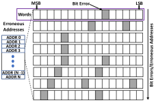
In strategy 2, we sort all the error-prone MRAM addresses in ascending order with decreasing quality (increasing number of errors) according to the total number of bit errors present in each word based on the occurrence and bit positions of the errors. A larger number of bit errors at the most significant bits (MSB) position denote higher application quality degradation; therefore, those addresses are assigned to lower-level positions. Besides, bytes/half-words can also be chosen instead of words (if required) as the error granularity. This decision depends entirely on the stored data’s nature and can be trivially extended. Fig. 3 depicts the sorting strategy. Data allocation is performed to each address in the sorted order, i.e., data is first assigned to the least erroneous addresses and later to addresses with higher errors ensuring that at reduced the stored data always incurs the least amount of errors. However, each application’s critical data must be allocated to entirely accurate addresses. Experimental results reveal that the enormous amount of accurate addresses is sufficient for most applications. Next, approximate data can be allocated to either accurate (based on availability) or erroneous addresses sorted according to the number of errors. As (i) sorting the erroneous addresses require extra overhead and complexity and (ii) most of the big data applications, the performance of strategy 1 is sufficient enough (see Sect. 5.3), so we propose strategy 2 in this work for further performance enhancement111Results of strategy 2 are not presented in this work as we achieve almost accuracy only using strategy 1. (if required).
5 Experimental Setup, Results, & Analysis
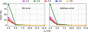
The preliminary analysis is performed over ten (2 chips from each MR0A16ACYS35, MR0A16AYS35, MR1A16AYS35 MR2A16ACYS35, MR2A16AYS35 models) 16-bit parallel interfaced differently sized () toggle MRAM chips to verify our proposed scheme. These chips belong to Everspin technologies. Among them, five chips are selected randomly to perform extensive analysis to verify our observations’ true universality. The characterization is performed using our custom memory controller implemented on the Alchitry Au development board containing Xilinx Artix 7 (XC7A35T-1C) FPGA to manipulate different timing latency of a couple of emerging memories [16]. The temperature (low/high) experiments were performed by placing the memory socket that holds the memory chip in Temptronic ATS-605 ThermoStream to maintain a uniform temperature.
According to Sect. 4.2, the generated errors are pattern-dependent on reduced write operation. Therefore, to determine the suitable pattern and examine the data pattern dependency, a total of 5-set measurement data is collected with seventeen different intuitive (solid) and non-intuitive (random, checkerboard, and striped) 16-bit input data patterns: (0xFFFF, 0xAAAA,0x5555, 0x0000) from each ten memory chips222The least significant 8 bits of the address-bit are used for column addressing for all memory chips. before performing characterization. We observed that, at reduced , switching from “1” to “0” produces more bit-error in our test MRAM chips. Consequently, the reduced produces maximum bit-error with the solid 0x0000 pattern when the memories are initialized with logic “1”. Therefore, we initialized memory with “1” for all test patterns (except for the solid 0xFFFF test pattern) to simulate the worst possible usage scenario. Based on the observation and the discussion on Sect. 4.2, we also conclude that the parallel (anti-parallel) configuration is the logic state ’1’ (state ’0’). Next, to characterize the MRAM cells (discussed in Sect. 4.2), we collected a total of 50-set measurement data with only solid 0x0000 input pattern from the randomly selected five memory chips. We chose the value of , of the recommended , for this work to obtain approximate writes. However, our selected value of can generate a sufficient number of accurate addresses (a moderate number of incorrect outputs) for the proposed framework.
Analyzing results from the conducted experiments validate our proposed scheme’s novelty and provide interesting insights. The results are divided into five broad subsections. In the first part, we manifest the speed-quality (number of erroneous cells/addresses) trade-off for selecting the reduced appropriately, a universal trait in any approximate computing mechanism. The second part presents the characterization results in detail applying Algo. 1. The third part shows how the output quality is affected when data is written into the memory with different initialized values and with or without applying the proposed address selection strategy (strategy 1 of Algo. 1). We also show that our approach results in comparably higher performance improvement than many popular (non) volatile memory-based prior works [8, 9, 10, 12]. Moreover, an efficient implementation of a memory controller can further improve the overall performance of our proposed framework. Note that all results are presented in the Sects. 5.2 and 5.3 are obtained at room temperature (). The fourth part describes the approximate MRAM results subject to operating conditions and memory chip variations. Finally, the fifth part elucidates our proposed technique’s power analysis results.
5.1 Selection of
An extensive analysis is performed to determine the error profile, such as frequency, location of the bit errors, comparing the behavior of the faulty/erroneous outputs at different reduced values using solid 0x0000 data pattern. We reduce the value from (manufacturer’s recommended) to , , and , respectively (Fig. 4). Note that our experimental setup’s timing resolution is limited to . At = , the total failed bit counts fall within – , which spans over – addresses. Our analysis shows that higher bit errors can be used for random number generation and physical unclonable function [33] but is not suitable for approximate computing. However, at = and , the obtained total failed bits are almost negligible ( and , respectively) for all ten chips (considering a single measurement). Hence, we choose = (considering the number of failed bit counts) to characterize erroneous cells to improve write speed ( overall improvement) and power savings (see Sect. 5.5).
5.2 Characterization of Error-Prone Cells
The cell characterization of MRAM is performed according to Sect. 4.2 with temporal measurements. Solid 0x0000 is used as the write data pattern. Moreover, the entire memory is reset with the solid 0xFFFF data pattern before every measurement to erase previously written data traces. In Table I, the first two rows show the statistics of erroneous MRAM addresses and bits after performing the proposed cell characterization algorithm (strategy 1 of Algo. 1). Here, is the percentage of total erroneous addresses, and is the percentage of total erroneous bits accumulated from 50 temporal measurements (obtained through characterization). The results manifest that the total number of erroneous bits obtained at reduced () varies from chip to chip. We also observe that only a few addresses hold these erroneous bits. The rest of the rows represent erroneous addresses and bits from different data patterns and to which extent they belong to and . Here, is the percentage of total erroneous addresses, and is the percentage of total erroneous bits from a specific test pattern (from a single measurement), and is the percentage of belonging to . Similarly, is the percentage of belonging to .
Table I represents that, after performing characterization using temporal measurements with solid 0x0000 data pattern, the cumulative amount of erroneous addresses is , and bits is for chip 1 (C1). During the testing phase, the number of erroneous addresses observed using solid 0x0000 data pattern is only , and bits is only . Now, among these erroneous addresses, of addresses belong to the , and of bits belong to the .
In summary, the cumulative maximum amount of erroneous addresses is , whereas the minimum is only (\nth1 row of characterization segment in Table I) for different memory chips at . Similarly, in Table I, the cumulative maximum amount of erroneous bit is , whereas the minimum is only (\nth2 row of characterization segment). This indicates that of the addresses ( of bits) are entirely accurate in the worst case scenario, resulting in negligible or no loss in output quality. As the percentage of error-prone addresses is fairly small () regardless of memory size, storage overhead is minimal for storing these few memory addresses’ information.
For pattern 0xAAAA or 0x5555, we do not observe any error for any data pattern. Based on the internal architecture of MRAM, there might be different reasons behind not getting any error. For example, if all of the I/O buffers are driven by the same power rail, the inrush current caused by the I/O buffers should be lower for these specific data patterns as only 8 out of 16 bits experience the switching [35]. Hence, the overall timing characteristics might be improved [35]. Moreover, the maximum obtained erroneous address () is , whereas the minimum is only for any given pattern considering a single test measurement. Similarly, the maximum obtained erroneous bit () is , whereas the minimum is only . Besides, our proposed characterization technique covers most erroneous addresses () and bits () for all data patterns. We observed that the lowest covered erroneous address () is and bit () is for solid 0xFFFF data pattern. However, a closer observation reveals that solid 0xFFFF data pattern produces only erroneous addresses and erroneous bits, which is negligible (). This insignificant number of errors can be overlooked for any big data application.
| Sample Chip33footnotemark: 3 | (%) | C1 | C2 | C3 | C4 | C5 | |
| Characterization | 22.41 | 26.41 | 10.34 | 8.36 | 5.33 | ||
| 10.49 | 22.06 | 7.60 | 5.15 | 3.89 | |||
| Solid | FFFF | 0.26 | 0.26 | 0 | 0 | 0 | |
| 0.11 | 0.23 | 0 | 0 | 0 | |||
| 1.74 | 60.81 | —- | —- | —- | |||
| 2.76 | 54.39 | —- | —- | —- | |||
| 0000 | 2.52 | 6.04 | 1.83 | 2.04 | 1.29 | ||
| 0.83 | 3.30 | 1.25 | 1.36 | 0.86 | |||
| 96.92 | 99.28 | 95.26 | 86.23 | 94.34 | |||
| 85.48 | 98.36 | 94.37 | 80.73 | 91.5 | |||
| Row Striped | FFFF | 1.99 | 3.52 | 0.72 | 0.82 | 0.62 | |
| 0.67 | 2.13 | 0.53 | 0.56 | 0.47 | |||
| 97.78 | 99.55 | 95.2 | 92.87 | 95.78 | |||
| 90.9 | 98.34 | 94.42 | 91.43 | 94.11 | |||
| 0000 | 0.75 | 2.63 | 0.94 | 1.09 | 0.67 | ||
| 0.18 | 1.25 | 0.61 | 0.68 | 0.40 | |||
| 97.77 | 99.45 | 96.8 | 84.29 | 94.03 | |||
| 83.07 | 98.55 | 96.02 | 76.87 | 90.46 | |||
| Column Striped | FFFF | 1.68 | 0 | 1.06 | 1.27 | 0.89 | |
| 0.67 | 0 | 0.71 | 0.79 | 0.60 | |||
| 87.4 | — | 93.13 | 90.23 | 89.82 | |||
| 74.8 | — | 92.75 | 89.73 | 88.73 | |||
| 0000 | 1.37 | 1.18 | 0.32 | 0.37 | 0.22 | ||
| 0.54 | 0.94 | 0.19 | 0.20 | 0.12 | |||
| 46.99 | 90.73 | 51.74 | 32.89 | 34.93 | |||
| 47.51 | 93.23 | 51.25 | 29.09 | 35.42 | |||
| Checker- board | FFFF | 1.59 | 3.05 | 0.71 | 0.84 | 0.61 | |
| 0.60 | 1.77 | 0.51 | 0.53 | 0.41 | |||
| 76.3 | 96.02 | 83.44 | 74.97 | 79.47 | |||
| 68.07 | 93.81 | 83.96 | 76.62 | 80.64 | |||
| 0000 | 1.25 | 2.96 | 0.64 | 0.75 | 0.49 | ||
| 0.59 | 1.55 | 0.40 | 0.42 | 0.29 | |||
| 62.61 | 96.02 | 85.71 | 83.54 | 81.54 | |||
| 60.43 | 93.62 | 83.97 | 82.49 | 79.89 | |||
| Any Pattern44footnotemark: 4 | 5555 / AAAA | 0 | 0 | 0 | 0 | 0 | |
| 0 | 0 | 0 | 0 | 0 | |||
| —- | —- | —- | — | — | |||
| —- | —- | —- | — | — | |||
| Random | 0.27 | 0.28 | 0.22 | 0.19 | 0.16 | ||
| 0.13 | 0.13 | 0.11 | 0.42 | 0.08 | |||
| 34.83 | 68.94 | 13.97 | 10.18 | 10.12 | |||
| 20.99 | 62.47 | 11.5 | 7.55 | 8.02 | |||
| ∗NB. —- not performed as no error occurred at reduced for corr- | |||||||
| esponding data patterns. | |||||||
Note that taking the union of the errors resulting from each data pattern (0xFFFF, 0xAAAA,0x5555, 0x0000) can further improve the fault coverage for the worst case. However, only a marginal improvement is observed for the chips used for experiments using different data patterns over the solid 0x0000 data pattern. Besides, Table I shows that a vast portion of the erroneous addresses () generated from different data patterns belongs to those erroneous addresses () obtained through the address selection strategy from error characterization using solid 0x0000 data pattern (described in strategy 1 of Algo. 1). Furthermore, it is essential to note that the acquired erroneous addresses heavily depend on the training data and frequency characteristics. Hence, it becomes imperative to select the training data and frequency judiciously.
5.3 Evaluation
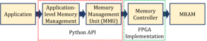
We evaluate our proposed AC framework with two different end-user applications- (i) JPEG image compression and (ii) optical character recognition (OCR) using the K-nearest neighbors (KNN) algorithm [12]. Fig. 5 presents the evaluation scheme for our proposed AC framework. We use this scheme to emulate MRAM as the main memory for both applications. Conventionally, memory allocation/deallocation (resource management) is accomplished at the application level with the assistance of the operating system (application-level memory management) [36]. On the other hand, a memory management unit (MMU) is a separate entity responsible for translating virtual addresses into physical addresses. Although traditionally, MMU is a hardware unit, software implementation of memory management is also feasible without requiring virtual addresses[37]. To simplify our experimental setup, we fuse the resource manager and the MMU in a single python API (similar to [37]). This python API also interfaces our custom memory controller, built on an FPGA board.
For JPEG application, we use the most common and popular metrics, signal-to-noise ratio (SNR), mean squared error (MSE), and peak signal-to-noise ratio (PSNR), between the approximated image and the unapproximated image used in the JPEG compression to quantify the acceptability of the application output quality. The SNR, MSE, and PSNR are calculated using the following equations (Eqs. 1 to 3). Here, and are the compressed JPEG image data with and without applying our AC framework, respectively. Note that the size of the images is , where . Besides, is the maximum possible pixel value of the image. Here, the pixels are represented using 8 bits per sample; hence, .
| (1) |
| (2) |
| (3) |
The value of SNR, MSE, and PSNR measures the image’s quality of JPEG compression output, evaluating the proposed scheme’s effectiveness. A minimum SNR value is required for such applications for the approximated image where the human brain and eyes can differentiate between the approximated and unapproximated image. A lower SNR value is considered as unacceptable output quality and vice versa. Similarly, a higher MSE value is considered as unacceptable output quality. The SNR, MSE, and PSNR measurements reveal the degree to which an application could produce satisfactory and reasonable output at reduced for approximate applications and determine the achievable limits of the performance and power improvements for MRAM technology. Fig. 6 shows the unapproximate and approximate output image quality with and without applying the proposed addresses selection technique (strategy 1 of Algo. 1), considering two different initialization states. The SNR of the image is infinite (MSE of the image is zero) means it does not have any errors relative to the unapproximated image output (Table III). Observing the images and the related SNR and MSE reveals the appropriateness of the proposed technique through application quality.
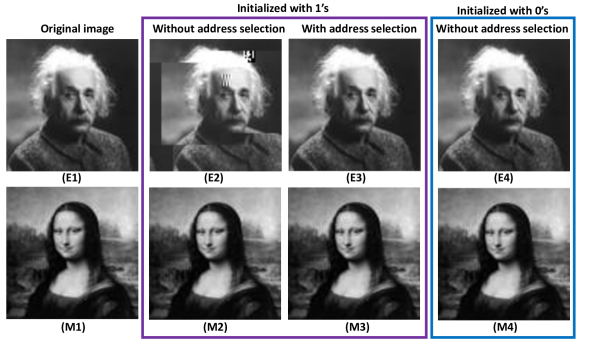
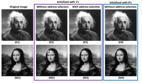
We have presented our results with and without the address selection technique in this work. In the “without address selection” technique, our proposed framework produces the worst possible result, where we did not consider erroneous and error-free addresses differently, i.e., memory is allocated conventionally. On the other hand, in the “with address selection” technique, we excluded error-prone addresses during memory allocation (strategy 1 of Algo. 1). Note that we did not perform a detailed analysis using sorted addresses (obtained using strategy 2 of Algo. 1) as reducing causes at most error in a single measurement. This strategy would only be required when the application needs the entire memory address. Therefore, we did not allocate data based on (lower or higher) error locations. Additionally, this strategy will also include a higher system overhead.
The result shows the influence of address selection on application quality, which is necessary to understand the impact of approximate data placement in memory addresses. This, in turn, is useful to comprehend how application quality changes with initialized values. In Fig. 6, the \nth2 & \nth3 columns show the JPEG image without and with applying the address selection technique, respectively. It is evident that the image quality improvement obtained using the proposed address selection technique is substantially better than without applying the technique, underscoring the need for the proposed address selection. However, as switching from “1” “0” is more vulnerable at reduced , requiring more write current for the prolonged duration; hence, initializing the entire memory with all 1’s requires address selection technique to attain very small or no loss in the output quality. Contrarily, initializing the entire memory with all 0’s does not require an address selection technique to obtain the same level of output quality. Furthermore, we also observe that commercial-grade MRAM is more vulnerable to reduced than industrial-grade MRAM as commercial-grade MRAM is more susceptible to thermal noise (see Sect. 5.4). Therefore, without applying the address selection technique in industrial-grade MRAMs, we notice a negligible loss in the output quality. It is worth mentioning that JPEG compression is a critical application in approximate computing. For example, a slight change in the RUNLENGTH (number of consecutive zero-valued discrete cosine transform (DCT) coefficient of the compressed JPEG data [38]) can impact the output quality severely.
In addition to JPEG image compression, we also demonstrate our AC framework for the KNN algorithm. KNN algorithm is a widely used supervised machine learning technique for image classification and object recognition (detail construction of the algorithm is out of this paper’s scope). In this work, we use the UCI optical character recognition (OCR) dataset [39] and the KNN algorithm (vanilla). To evaluate the performance of our proposed framework, we compare KNN accuracy with and without using our AC framework. Accuracy quantifies the fraction of correct prediction out of all test samples. The accuracy of the KNN algorithm without using our AC framework is . If the MRAM is initialized with logic “0” bits, our AC framework does not impact the KNN accuracy. On the other hand, with the logic “1” initialization and without address selection technique, the accuracy of the KNN algorithm using our AC framework ranges between to (i.e., performance degradation). With the logic “1” initialization and address selection technique, however, the accuracy of the KNN algorithm with our frameworks improves to at least (i.e., performance degradation).
5.4 Effect of Operating Condition and Chip Variations
Random thermal fluctuations and process variation exacerbate the intrinsic stochasticity of the magnetic orientation switching of MRAM cells; hence, significantly varies the switching time of the cell over the entire memory array. Therefore, the MRAM write failure rate increases significantly as temperature increases [40]. We can characterize these failures at the highest possible operating temperature to incorporate the temperature effect to cover maximum erroneous addresses. Our observation is that errors occurring at a lower temperature are a subset of those occurring at high temperatures; therefore, guaranteeing no additional bit errors in the lower temperature range. The highest temperature used for characterization can be determined within the manufacturer’s recommended value covering all MRAM models (in our case, ), suitable for commercial applications. Our experiments’ characterization and evaluation are performed at room temperature (). To demonstrate the temperature effect on MRAM errors, we evaluate results for both high () and low () temperatures and compare them with room temperature ().
We observe that the total number of errors and erroneous addresses increase with higher temperatures. However, no significant change is observed in the total number of erroneous addresses at low temperature () and temperature range up to . As the thermal noise becomes smaller at low temperature, the low temperature has less impact at reduced . Therefore, only results at temperature (worst case) are shown in Table II as the obtained errors are insignificant at low temperatures. Moreover, the maximum erroneous address () at in reduced () is for any given pattern (except 0xAAAA or 0x5555), considering a single test measurement for all memory chips. In contrast, the minimum is only . Similarly, the maximum erroneous bit () is , whereas the minimum is only . Comparing with the nominal operating condition (Table I), we observe a maximum of increase in the erroneous addresses and increase in the erroneous bits at temperature. Contrarily, the maximum erroneous address () at in reduced () is . In contrast, the minimum is only . Similarly, the maximum erroneous bit () is , whereas the minimum is only . Comparing with the nominal operating condition (Table I), we observe a maximum of decrease in the erroneous addresses and decrease in the erroneous bits at temperature. Although a detailed assessment is not performed, the obtained results reveal that errors at lower temperatures are a subset of the errors at high temperatures.
Furthermore, to observe the impact of external magnetic field (M-Field), we collected a set of test data sequences at room temperature () with an external M-Field by using a set of permanent magnets in six different orientations of 3D coordinates555The maximum recommended magnetic field is for commercial-grade and for industrial-grade MRAM.. However, no significant change is observed in the number of erroneous cells with () external M-Field. The maximum erroneous address () in reduced () is . In contrast, the minimum is only . Similarly, the maximum erroneous bit () is , whereas the minimum is only . Comparing with the nominal operating condition (Table I), we observe a maximum of increase in the erroneous addresses and increase in the erroneous bits. Hence, we can conclude that the external M-Field does not significantly impact the number of error occurrences.
The silicon results from five different memory models of three different sizes show that the statistics of erroneous cells are different for different memory models, shown in Tables I and II. These sources of variations come from architectural as well as both inter- and intra-chip dissimilarities due to the random process variation, which is the key source of any memory chips’ randomness. Data collected from different FPGAs also verify that the memory controllers do not influence the proposed framework.
| Sample Chip | (%) | C1 | C2 | C3 | C4 | C5 | |
| Solid | FFFF | 0.002 | 0.09 | 0 | 0 | 0 | |
| 0.002 | 0.02 | 0 | 0 | 0 | |||
| 100 | 5.79 | —- | —- | —- | |||
| 100 | 16.77 | —- | —- | —- | |||
| 0000 | 16.00 | 13.53 | 7.55 | 2.73 | 0.94 | ||
| 6.31 | 7.54 | 4.30 | 0.56 | 0.22 | |||
| 39.70 | 77.63 | 10.72 | 11.77 | 21.8 | |||
| 26.59 | 74.68 | 7.93 | 17.07 | 32.54 | |||
| Row Striped | FFFF | 12.83 | 6.92 | 4.63 | 1.61 | 0.33 | |
| 6.05 | 3.87 | 1.85 | 0.35 | 0.12 | |||
| 47.39 | 81.38 | 13.84 | 15.64 | 38.17 | |||
| 32.07 | 79.25 | 13.31 | 21.56 | 42.08 | |||
| 0000 | 12.79 | 5.74 | 2.87 | 1.01 | 0.167 | ||
| 5.61 | 3.07 | 1.33 | 0.21 | 0.07 | |||
| 30.32 | 78.44 | 6.74 | 5.91 | 14.65 | |||
| 18.65 | 73.35 | 3.11 | 9.61 | 22.77 | |||
| Column Striped | FFFF | 15.56 | 9.93 | 3.55 | 1.02 | 0.273 | |
| 8.98 | 5.41 | 1.04 | 0.24 | 0.12 | |||
| 47.66 | 74.21 | 12.32 | 16.07 | 48.42 | |||
| 27.41 | 68.75 | 15.01 | 23.16 | 53.61 | |||
| 0000 | 3.15 | 2.13 | 2.55 | 0.83 | 0.23 | ||
| 0.76 | 0.93 | 0.68 | 0.15 | 0.09 | |||
| 28.25 | 95.81 | 9.32 | 14.93 | 36.38 | |||
| 41.57 | 94.11 | 14.83 | 23.5 | 37.36 | |||
| Checker- board | FFFF | 9.40 | 5.93 | 3.34 | 0.84 | 0.23 | |
| 4.75 | 3.21 | 0.86 | 0.20 | 0.11 | |||
| 50.53 | 80.52 | 12.11 | 17.01 | 48.17 | |||
| 33.8 | 75.31 | 16.94 | 26.46 | 53.5 | |||
| 0000 | 9.10 | 5.96 | 3.37 | 0.89 | 0.25 | ||
| 4.37 | 3.06 | 0.93 | 0.19 | 0.11 | |||
| 40.51 | 78.21 | 8.82 | 14.67 | 41.71 | |||
| 24.48 | 71.84 | 12.77 | 22.76 | 41.62 | |||
| Any Pattern | 5555/ AAAA | 0 | 0 | 0 | 0 | 0 | |
| 0 | 0 | 0 | 0 | 0 | |||
| —- | —- | —- | —- | —- | |||
| —- | —- | —- | —- | —- | |||
| Random | 0.13 | 0.23 | 0.01 | 0.005 | 0.008 | ||
| 0.04 | 0.09 | 0.01 | 0.002 | 0.002 | |||
| 59.09 | 72.97 | 31.43 | 38.46 | 38.1 | |||
| 33.16 | 63.81 | 36.3 | 40.48 | 41.58 | |||
| ∗NB. —- not performed as no error occurred at reduced for corr- | |||||||
| esponding data patterns. | |||||||
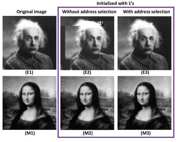
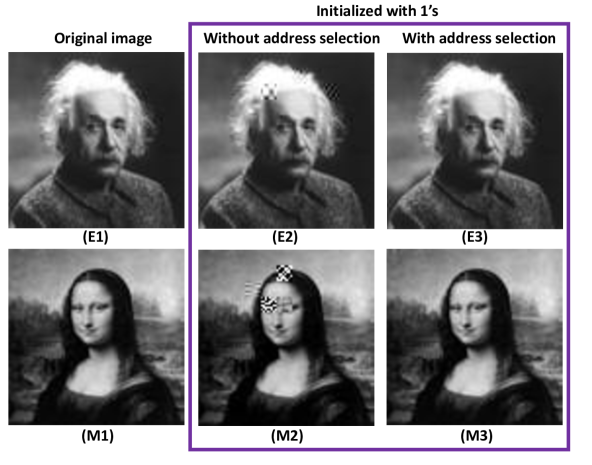
Furthermore, we have also evaluated our result for both JPEG compression and the KNN algorithm at high temperature (). Fig. 7 presents the JPEG images at with “1” initialization (initialization “0” has no impact). Compared with Fig. 6, the image quality is slightly worse (noise magnitude increased by ). On the other hand, the KNN accuracy further decreased by (at most). Table III summarizes the list of applications, datasets, and results at both room temperature () and high temperature ().
| Chip grade | Commerical | Industrial | |||||||||||||||||
| Operating condition | () | () | () | () | |||||||||||||||
| Initial state | “1” | “0” | “1” | “0” | “1” | “0” | “1” | “0” | |||||||||||
| App. | Algorithm | Approx. data | Quality metric | Addr. sel. | Addr. sel. | Addr. sel. | Addr. sel. | Addr. sel. | Addr. sel. | Addr. sel. | Addr. sel. | ||||||||
| W/O | W | W/O | W | W/O | W | W/O | W | W/O | W | W/O | W | W/O | W | W/O | W | ||||
| JPEG comp. | JPEG enc. | JPEG image | SNR | 4.34 | 4.35 | 122.00 | 36.99 | ||||||||||||
| MSE | 3216.11 | 0.00 | 0.00 | 0.00 | 3208.83 | 0.06 | 0.00 | 0.00 | 111.52 | 0.85 | 0.00 | 0.00 | 339.17 | 1.01 | 0.00 | 0.00 | |||
| PSNR | 13.06 | 13.07 | 60.40 | 27.66 | 48.85 | 22.83 | 48.09 | ||||||||||||
| OCR | KNN | Feat. vec. | % Acc.* | 88.25 | 92.75 | 95.5 | 95.5 | 85.25 | 91.75 | 95.5 | 95.5 | 92.25 | 93.5 | 95.5 | 95.5 | 92.00 | 92.75 | 95.5 | 95.5 |
| *KNN Accuracy (Acc.) without approximation = 95.5%; W/O: without address selection; W: with address selection | |||||||||||||||||||
5.5 Power Improvement
MRAM write energy () can be expressed as by Eq. 4. Here, is the write pulse magnitude, is the write current that depends on instantaneous cell resistance () during the resistance switching process. A higher value of will cost a higher .
| (4) |
To evaluate the energy efficiency of our proposed framework, we require to measure the write current over . However, it is difficult to achieve an appropriate experimental setup using COTS chips. For example, all of our test chips have multiple pairs of power-ground pins. Therefore, measuring write current requires probing each power/ground current with sufficiently high-frequency bandwidth instruments while preserving precise timestamps. Additionally, power consumed by memory peripherals (I/Os, sense-amplifier, etc.) is hard to estimate. Therefore, we estimate the power savings of our AC scheme from simulation data. For power analysis, we use the simulation framework for Spin-Transfer Torque MRAM (STT-MRAM), developed by Wang et al. [41]. It is worth mentioning that STT-MRAM is an improved version of MRAM technology, which is more scalable, hence achieving higher densities at a lower price, providing a significant reduction in switching energy and consuming low power compared to toggle MRAM devices. In STT-MRAM, the current is injected perpendicularly into the magnetic tunnel junction (MTJ), and the read/write operation is performed through the same path [42, 43]. Our simulation result aligns with the error characteristics of toggle MRAM (see Sect. 5.2), confirming our proposed AC framework’s applicability in next-generation MRAM technology. Note that all simulation parameters in this work are adopted from [41] and [44], including physical variation (MTJ tunnel thickness, free layer thickness, cell area, etc.) that might occur from the fabrication process.
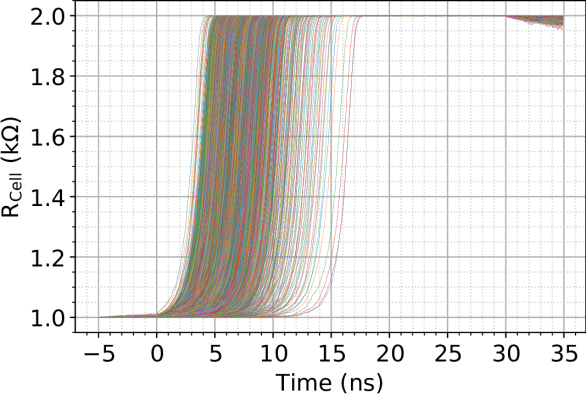
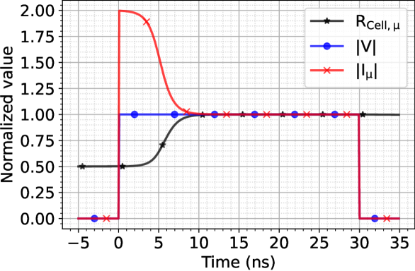
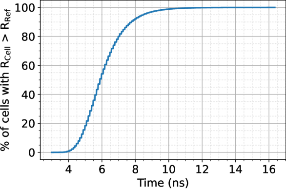
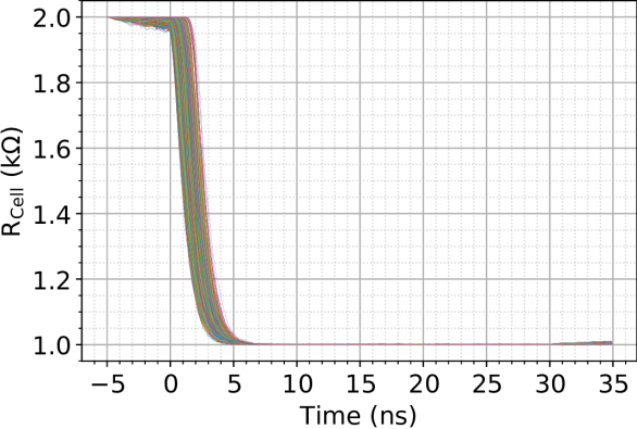
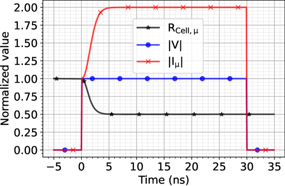
We summarize our simulation result in Fig. 8, performed over STT-MRAM cells. Figs. 8(a)–8(c) represent MRAM switching characteristics for low to high resistance (normalized). On the other hand, 8(d)–8(f) show the opposite switching characteristics (i.e., ). Fig. 8(a) and 8(d) show the cell resistance () over for all memory cells. These figures prove that switching the low resistance state (logic “1”) to the high resistance state (logic “0”) is more critical (higher transition time) than the high to low resistance state switching, which we also observe from our experimental result. The should be sufficiently large to guarantee proper switching of all cells under all kinds of physical variation. From this simulation statistics, if we want to guarantee write success ( write failure out of write operations), the should be at least . The also depends on operating conditions. For example, with voltage variation ([45]) and write accuracy, the increases to . In this discussion, we will consider as the write time for standard operation.
Figs. 8(b) and 8(e) represent mean (normalized) cell resistance (), write pulse voltage (), and write current (). In these figures, mean write energy is proportional to the area under curve (as is constant). Fig. 8(c) and 8(f) represent the cumulative distribution function (CDF) of at which the memory cells switch the side of (i.e., or ). For , all memory cells switch their side of within . However, for , of cells switch their side of within and of cells switch their side within . Therefore, in this simulation, applying would produce almost similar to our experimental result (obtained at ). Fig. 8(b) and 8(e) show that ( curve), with , the mean energy saving would be for transition and for transition (considering energy at ). Therefore, the average energy saving would be , considering the uniform distribution of logic “0” and logic “1” in application data. Note that the energy-saving would be more for a tighter estimation of .
Table IV compares our proposed technique with MRAM-based prior approximate computing frameworks. As previous works are based on simulating STT-MRAM, we use our STT-MRAM-based simulation result for a fair comparison. The \nth2 () and \nth3 () columns of the table represent the reduction of write pulse width () and write energy. The \nth4 column shows the error (bit error rate or ) induced in approximate computing. The result shows that our proposed technique produces superior results over [8], considering , , and . On the other hand, the AC framework proposed by Ranjan et al. can save more power with smaller [28, 12]; however, it does not improve the write speed. Additionally, our proposed technique can be readily used in COTS available MRAM and does not require any modification on system architecture.
5.6 Summary of Results
Overall, we draw the following main conclusions from the results.
-
1.
The cell characterization is performed once in a lifetime before deploying the MRAM in the computing system. However, the appropriate selection is required for the training data and frequency to perform characterization.
-
2.
The output quality degradation occurs when approximate application data are placed at addresses containing both erroneous and error-free (without address selection). However, this is the worst possible scenario when the entire memory is initialized with all 1’s before writing. However, with the proposed address selection strategy, we can achieve almost of output quality.
-
3.
Contrarily, the same applications retain almost of quality even when put into addresses containing both erroneous and error-free in the case when the entire memory initialized with all 0’s before writing.
-
4.
Commercial-grade MRAM is more vulnerable to reduced than industrial-grade MRAM
-
5.
Errors that occurred at lower temperatures are a subset of the errors at high temperatures.
-
6.
Our simulation result shows that our proposed framework will also be applicable for STT-MRAM. The simulation also shows that the reduced write pulse width () can also save on average of write energy (considering write accuracy with nominal ) with virtually no loss in output quality for error-resilient applications.
6 Discussions
6.1 Storage and Performance Overheads
Our proposed framework requires allocating application data (critical and approximate) to first error-free addresses and moving forward to erroneous addresses based on the required application accuracy. We use a similar approach proposed in [10]; however, our approach is simpler as the access policy of DRAM and MRAM is entirely different, and we do not require quality-wise erroneous address sorting. Note that the following strategy needs to be performed only for high-accuracy applications when no more accurate addresses are available. For this purpose, a custom memory allocator (resource manager) is required to track the erroneous addresses obtained from the characterization step. Next, based on the application requirements, it will allocate the user annotated critical and approximate data into virtual addresses using a critical bit for each address. Operating systems (OS) usually accomplish mapping virtual to physical addresses through a page table (with the assist of MMU). Hence, in our proposed scenario, the OS has to perform this additional responsibility of assigning virtual to physical addresses belonging to error-free (accurate) and erroneous addresses depending on the application requirement.
The OS and the MMU require additional logic to implement the proposed addresses selection strategy. Towards this end, first, the OS can track the erroneous addresses using a custom data structure (consisting of critical bits). Then, at the start-up phase, the OS can utilize the custom data structure to modify the core map and subsequently utilize this modified mapping function to translate virtual to a physical address. Note that the modified mapping is used in conjunction with the original core map. Before performing virtual to physical address mapping, first, the OS will check whether the virtual address is critical or not for the required application. If it is critical, the OS will check for the error-free address based on the application requirement as specified by the system designer. In addition to that, one can use additional flag bits on the cache memory (similar to the valid bit) to identify if a data block is erroneous or accurate. This flag bit can be directly copied from the custom data structure in parallel to the main memory operations. The OS can utilize this flag bit during the memory allocation for further optimization. It is expected that the OS will completely automate the entire allocation process for the proposed framework. Hence, hardware and OS support are essential for adapting approximate MRAM to reality in sophisticated high-end embedded computing systems. However, a software-based memory management can further simplify our framework as it does not require any virtual to physical address mapping [37]. Note that for a 1GByte main memory (with 32Byte block size), the size of the custom data structure would be 4MByte. It is worth mentioning that the latency and energy overheads for the MRAM characterization are negligible as the characterization needs to be performed only once before deploying the MRAM in the computing system.
6.2 Critical Data Protection: MRAM as a Cache
A significant challenge of approximate storage usage is: most of the highly amenable approximate computing paradigm applications also have a mixture of control data (i.e., critical data) that is intolerable to any errors. Hence imposing approximation on these data makes them unreliable. For example, the instruction cache requires to be entirely error-free. Although various solutions are proposed to protect the critical data part [8], the critical data size is minimal compared with the non-critical counterpart. Therefore, designing a heterogeneous data cache memory array with different static (design-time) and dynamic (runtime) configurations to make critical data error-resilient guarantees error-free operation. However, this requires (i) fabrication parameters modification (ii) complex cache controller for proper data allocation in different arrays. Contrarily, a more straightforward solution for critical data protection is either using multiple copies of this data content or an error correction code (ECC), where data protection is performed through additional check bit(s). However, the overhead due to the additional bit-cells for the mentioned approaches is minimal for these significantly smaller critical data sizes [8]. Besides, considerably lower write accesses to the instruction cache help the critical data protection considerably more manageable for our proposed framework.
6.3 Applicability to Next Generation MRAMs
We used COTS toggle MRAM, which is designed to act like SRAM. On the other hand, STT-MRAM performs like a persistent DRAM. The \nth1 generation STT-MRAM structure uses an in-plane MTJ (iMTJ), whereas \nth2 generation STT-MRAM devices use a more optimized structure known as perpendicular MTJ (pMTJ) in which the magnetic moments are perpendicular to the silicon substrate surface [43]. Therefore, \nth2 generation STT-MRAM is more scalable and cost-competitive than \nth1 generation STT-MRAM, thus a more promising technology to replace DRAM and other memory technologies. Our simulation result presented in Sect. 5.5 (based on \nth2 generation STT-MRAM) confirms that our proposed AC framework is also applicable for STT-MRAM. Additionally, the DRAM-like operation of STT-MRAM can provide further opportunities to improve performance. The DRAM read/write operations are generally performed in burst mode, where 4 or 8 data words are accessed (read/write) in a single command. In burst mode, only the first write operation requires full write time, whereas the next consecutive write operations only require an additional write pulse for each data word. Therefore, reducing write pulse width () can improve huge performance.
On top of that, unlike STT-MRAM, the new spin-orbit torque MRAM (SOT-MRAM) technology switched the free magnetic layer by injecting an in-plane current in an adjacent SOT layer (typically made of heavy metal). Due to the current injection geometry, the read and write paths are decoupled. SOT-MRAM offers better performance in terms of speed (sub-ns switching speed), endurance, power, and read stability at the cost of a slightly degraded density. As the SOT-MRAM has a similar switching characteristic as the previous generation of MRAMs [42], we believe our system-level proposed approach also applies to future MRAM generations. In the future, we plan to explore the SOT-MRAM experimentally (or with simulation) to confirm our hypothesis.
7 Conclusion
This paper proposes an efficient approximate computing framework to evaluate the applicability of non-volatile COTS MRAM, a promising candidate for future computing platforms, through memory address’s error characterization by utilizing the internal write latency variation of MRAM to improve the power efficiency. Our methodology provides an optimal system-level implementation yielding a favorable performance and power vs. quality trade-off for error-resilient applications by devising efficient segregation strategies for the erroneous addresses while allocating approximate and critical data systematically. Our experimental results reveal that MRAM-based memory systems can achieve substantial power and performance benefits for negligible or no loss in application output quality. Furthermore, other emerging memory technologies can also adopt the proposed address selection strategy, a promising framework aspect.
References
- [1] J. A. Mandelman et al., “Challenges and future directions for the scaling of dynamic random-access memory (dram),” IBM Journal of Research and Development, vol. 46, no. 2.3, pp. 187–212, 2002.
- [2] Q. Xu, T. Mytkowicz, and N. S. Kim, “Approximate computing: A survey,” IEEE Design Test, vol. 33, no. 1, pp. 8–22, 2016.
- [3] J. Han and M. Orshansky, “Approximate computing: An emerging paradigm for energy-efficient design,” in 2013 18th IEEE European Test Symposium (ETS), 2013, pp. 1–6.
- [4] S. Ghosh et al., “Security and privacy threats to on-chip non-volatile memories and countermeasures,” in Proceedings of the 35th International Conference on Computer-Aided Design, 2016.
- [5] X. Fong et al., “Spin-transfer torque memories: Devices, circuits, and systems,” Proceedings of the IEEE, vol. 104, no. 7, pp. 1449–1488, 2016.
- [6] A. Jog et al., “Cache revive: Architecting volatile stt-ram caches for enhanced performance in cmps,” in Proceedings of the 49th Annual Design Automation Conference, 2012, p. 243–252.
- [7] X. Wu et al., “Hybrid cache architecture with disparate memory technologies,” in Proceedings of the 36th Annual International Symposium on Computer Architecture, 2009, p. 34–45.
- [8] N. Sayed, R. Bishnoi, and M. B. Tahoori, “Approximate spintronic memories,” J. Emerg. Technol. Comput. Syst., vol. 16, no. 4, Sep. 2020.
- [9] S. Liu, K. Pattabiraman, T. Moscibroda, and B. G. Zorn, “Flikker: Saving dram refresh-power through critical data partitioning,” SIGPLAN Not., vol. 46, no. 3, p. 213–224, Mar. 2011.
- [10] A. Raha et al., “Quality configurable approximate dram,” IEEE Transactions on Computers, vol. 66, no. 7, pp. 1172–1187, 2017.
- [11] I. J. Chang, D. Mohapatra, and K. Roy, “A priority-based 6t/8t hybrid sram architecture for aggressive voltage scaling in video applications,” IEEE Transactions on Circuits and Systems for Video Technology, vol. 21, no. 2, pp. 101–112, 2011.
- [12] A. Ranjan et al., “Approximate storage for energy efficient spintronic memories,” in 2015 52nd ACM/EDAC/IEEE Design Automation Conference (DAC), 2015, pp. 1–6.
- [13] M. Shoushtari, A. BanaiyanMofrad, and N. Dutt, “Exploiting partially-forgetful memories for approximate computing,” IEEE Embedded Systems Letters, vol. 7, no. 1, pp. 19–22, 2015.
- [14] J. S. Miguel, M. Badr, and N. E. Jerger, “Load value approximation,” in 2014 47th Annual IEEE/ACM International Symposium on Microarchitecture, 2014, pp. 127–139.
- [15] “Everspin 16-bit parallel interface mram,” accessed: 22 April 2021. [Online]. Available: www.everspin.com/parallel-interface-mram
- [16] J. Rajewski, “Alchitry au fpga development board,” accessed: 22 April 2021. [Online]. Available: alchitry.com/products/alchitry-au-fpga-development-board
- [17] Y. Kim et al., “Write-optimized reliable design of stt mram,” in Proceedings of the 2012 ACM/IEEE International Symposium on Low Power Electronics and Design, New York, NY, USA, 2012, p. 3–8.
- [18] S. Chatterjee et al., “A scalable design methodology for energy minimization of sttram: A circuit and architecture perspective,” IEEE Transactions on Very Large Scale Integration (VLSI) Systems, vol. 19, no. 5, pp. 809–817, 2011.
- [19] X. Wu et al., “Hybrid cache architecture with disparate memory technologies,” in Proceedings of the 36th Annual International Symposium on Computer Architecture, vol. 37, no. 3, New York, NY, USA, Jun. 2009, p. 34–45.
- [20] B. Wang et al., “Exploring hybrid memory for gpu energy efficiency through software-hardware co-design,” in Proceedings of the 22nd International Conference on Parallel Architectures and Compilation Techniques, 2013, pp. 93–102.
- [21] P. Zhou et al., “Energy reduction for stt-ram using early write termination,” in 2009 IEEE/ACM International Conference on Computer-Aided Design - Digest of Technical Papers, 2009, pp. 264–268.
- [22] S. P. Park et al., “Future cache design using stt mrams for improved energy efficiency: Devices, circuits and architecture,” in DAC Design Automation Conference 2012, 2012, pp. 492–497.
- [23] Y. Emre et al., “Enhancing the reliability of stt-ram through circuit and system level techniques,” in 2012 IEEE Workshop on Signal Processing Systems, 2012, pp. 125–130.
- [24] H. Naeimi et al., “Sttram scaling and retention failure,” in intel technology journal, vol. 17, no. 1, 2013.
- [25] A. Driskill-Smith et al., “Latest advances and roadmap for in-plane and perpendicular stt-ram,” in 2011 3rd IEEE International Memory Workshop (IMW), 2011, pp. 1–3.
- [26] C. W. Smullen et al., “Relaxing non-volatility for fast and energy-efficient stt-ram caches,” in 2011 IEEE 17th International Symposium on High Performance Computer Architecture, 2011, pp. 50–61.
- [27] A. Sampson et al., “Approximate storage in solid-state memories,” in 2013 46th Annual IEEE/ACM International Symposium on Microarchitecture (MICRO), 2013, pp. 25–36.
- [28] A. Ranjan et al., “Staxcache: An approximate, energy efficient stt-mram cache,” in Design, Automation Test in Europe Conference Exhibition (DATE), 2017, 2017, pp. 356–361.
- [29] D. Apalkov et al., “Magnetoresistive random access memory,” Proceedings of the IEEE, vol. 104, no. 10, pp. 1796–1830, 2016.
- [30] “Tmr sensors,” accessed: 22 April 2021. [Online]. Available: product.tdk.com/en/techlibrary/productoverview/tmr-angle-sensors.html
- [31] S. Kumar and P. K. Singh, “An overview of modern cache memory and performance analysis of replacement policies,” in 2016 IEEE International Conference on Engineering and Technology (ICETECH), 2016, pp. 210–214.
- [32] J. L. Hennessy and D. A. Patterson, Computer architecture: a quantitative approach. Elsevier, 2011.
- [33] F. Ferdaus et al., “True random number generation using latency variations of commercial mram chips,” in 2021 22nd International Symposium on Quality Electronic Design (ISQED), 2021, pp. 510–515.
- [34] R. Bishnoi et al., “Avoiding unnecessary write operations in stt-mram for low power implementation,” in Fifteenth International Symposium on Quality Electronic Design, 2014, pp. 548–553.
- [35] K. Shi and J. Li, “A wakeup rush current and charge-up time analysis method for programmable power-gating designs,” in 2007 IEEE International SOC Conference, 2007, pp. 163–165.
- [36] S. Pai, R. Govindarajan, and M. J. Thazhuthaveetil, “Fast and efficient automatic memory management for gpus using compiler-assisted runtime coherence scheme,” in 21st int. conference on Parallel architectures and compilation techniques, 2012, pp. 33–42.
- [37] D. Zagieboylo, G. E. Suh, and A. C. Myers, “The cost of software-based memory management without virtual memory,” arXiv preprint arXiv:2009.06789, 2020.
- [38] G. K. Wallace, “The jpeg still picture compression standard,” IEEE trans. on consumer electronics, vol. 38, no. 1, pp. xviii–xxxiv, 1992.
- [39] E. Alpaydin and C. Kaynak, “Optical recognition of handwritten digits data set,” 1998, accessed: 22 November 2021. [Online]. Available: archive.ics.uci.edu/ml/datasets/optical+recognition+of+handwritten+digits
- [40] F. Ferdaus and M. T. Rahman, Security of Emerging Memory Chips. Cham: Springer International Publishing, 2021, pp. 357–390.
- [41] S. Wang et al., “Comparative evaluation of spin-transfer-torque and magnetoelectric random access memory,” IEEE Journal on Emerging and Selected Topics in Circuits and Sys., vol. 6, no. 2, pp. 134–145, 2016.
- [42] C. Bi, N. Sato, and S. X. Wang, “6 - spin-orbit torque magnetoresistive random-access memory (sot-mram),” in Advances in Non-Volatile Memory and Storage Technology, 2019, pp. 203–235.
- [43] A. Khvalkovskiy et al., “Basic principles of stt-mram cell operation in memory arrays,” Journal of Physics D: Applied Physics, vol. 46, no. 7, p. 074001, 2013.
- [44] J. Song et al., “Evaluation of operating margin and switching probability of voltage-controlled magnetic anisotropy magnetic tunnel junctions,” IEEE Journal on Exploratory Solid-State Computational Devices and Circuits, vol. 4, no. 2, pp. 76–84, 2018.
- [45] M. Solka et al., “A practical methodology for calculating acceptable ir drop targets in advanced vdsm design.”
![[Uncaptioned image]](/html/2105.14151/assets/x18.jpg) |
Farah Ferdaus (S’20) received her M.S. degree in Electrical and Computer Engineering from the University of New Hampshire in 2018. She is currently working towards her Ph.D. in Electrical and Computer Engineering at Florida International University. Her research interests include performance enhancement and security solutions of emerging memories; privacy and security issues of existing memories; wireless communications and networks. |
![[Uncaptioned image]](/html/2105.14151/assets/Figures/BB.jpg) |
B. M. S. Bahar Talukder (S’18) received his Ph.D. degree in Electrical and Computer Engineering at Florida International University. His primary research interests include hardware security, secured computer architecture, machine-learning application in system security, and emerging memory technologies. |
![[Uncaptioned image]](/html/2105.14151/assets/x19.jpg) |
Md Tauhidur Rahman (S’12–M’18) is an Assistant Professor in the Department of Electrical and Computer Engineering at Florida International University (FIU). He received his Ph.D. degree in Computer Engineering from the University of Florida in 2017. His current research interests include hardware security and trust, memory system, machine learning applications, embedded security, and reliability. |