Understanding and minimizing resonance frequency deviations on a 4-inch kilo-pixel kinetic inductance detector array
Abstract
One of the advantages of kinetic inductance detectors is their intrinsic frequency domain multiplexing capability. However, fabrication imperfections usually give rise to resonance frequency deviations, which create frequency collision and limit the array yield. Here we study the resonance frequency deviation of a 4-inch kilo-pixel lumped-element kinetic inductance detector (LEKID) array using optical mapping. Using the measured resonator dimensions and film thickness, the fractional deviation can be explained within , whereas the residual deviation is due to variation of electric film properties. Using the capacitor trimming technique, the fractional deviation is decreased by a factor of 14. The yield of the trimming process is found to be 97%. The mapping yield, measured under a 110 K background, is improved from 69% to 76%, which can be further improved to 81% after updating our readout system. With the improvement in yield, the capacitor trimming technique may benefit future large-format LEKID arrays.
Lumped element kinetic inductance detectors (LEKIDs) have been widely developed for astronomical observations Day et al. (2003); Doyle et al. (2008); Adam et al. (2018); Wandui et al. (2020); Austermann et al. (2018); Wheeler et al. (2018); Walter et al. (2020) in the last decade. Their intrinsic frequency multiplexing property makes LEKIDs suitable for large detector arrays. In practice, the multiplexing factor per readout line depends on the readout bandwidth, resonance frequency spacing, and resonance width, which is usually limited by background radiation for ground-based observations. As the number of pixels per feedline increases, resonance frequency collision between adjacent resonators becomes problematic. When a collision happens, the readout tone may pick up signal from a nearby resonance. This affects the number of pixels that are useful for astronomical observations. Frequency collision is usually caused by the variation of material parameters, such as the film thickness, the superconducting transition temperature, and the resonator dimensions across the wafer. Aluminium is commonly used in LEKIDs design for its easy fabrication, low gap frequency and long quasiparticle lifetime Mazin (2020). Its low kinetic inductance and resistivity, however, impose thin films ( nm) and narrow linewidths ( ), in order to optimize sensitivity and optical coupling. For example, the NIKA2 260 GHz array uses a 18 nm thick Al film with a 4 inductor widthAdam et al. (2018). Intrinsic variation in these parameters gives rise to a large, uncontrolled deviation of the resonance frequency from the design values, leading to many frequency collisions. This causes the number of functional pixels of the NIKA2 260 GHz array to decrease from 84% to 70% under sky background illumination Adam et al. (2018).
Recently, a corrective technique has been developed, in which scatter in the resonance frequencies is mitigated by a second lithography step adapting the resonator capacitor Liu et al. (2017); Shu et al. (2018a). This technique has been deployed on LEKID arrays consisting of resonators. It has been shown that the deviation from design resonance frequency can be improved by a factor 10, going down from the few percent level to . Array yield has been shown to go up to 97% on a 1-inch 112-pixel array Shu et al. (2018a).
In this letter, we take this technique one step further, to a telescope-class, 4-inch kilo-pixel LEKID array. This array is designed for the 260 GHz band of the NIKA2 instrument with 2392 pixels, designed to have their resonance frequencies spaced by only 1.6 MHz. We have analysed the causes for resonance frequency deviation for 920 pixels from this array, and have applied our corrective technique to these pixels. We show that of the initial frequency deviation can be explained by geometric variations of the individual pixels, and that the technique is ready to be deployed on actual telescope-class arrays.
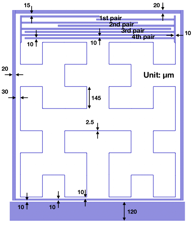
The detector array design in this study is based on the current NIKA2 array Calvo et al. (2016). To optimally take advantage of the angular resolution possible at the IRAM 30-m telescope, the meandering inductor is reduced to a surface area of Shu et al. (2018b). To fully cover the 80 mm diameter focal plane, the total number of pixels is increased to 2392, distributed over 8 feedlines. The resonators are made of nm thick Al on a -thick high-resistivity silicon substrate. In our design and calculations, we assumed a surface resistance and a surface inductance . A 200 nm thick Al film is deposited on the back side of the wafer, serving as the ground of the microstrip feedline and the backshort for optical coupling. The inductor is shaped in a 3rd-order Hilbert curve with a width of . An 8-finger interdigitated capacitor (IDC) is used to tune the resonance frequencies from , by decreasing the IDC finger lengths pair by pair. The geometry detail is shown in the supplementary material. On different feedlines, the number of resonators varies from 276 to 332 and the designed frequency spacing ranges from 1.51 MHz to 1.82 MHz. The resonance frequency shift due to coupling between adjacent resonators is optimized to be 55 kHz. The maximum crosstalk between feedlines is smaller than . The coupling quality factor is optimized to to match the expected internal quality factor under a sky radiation. The array design detail is shown in the supplementary material.
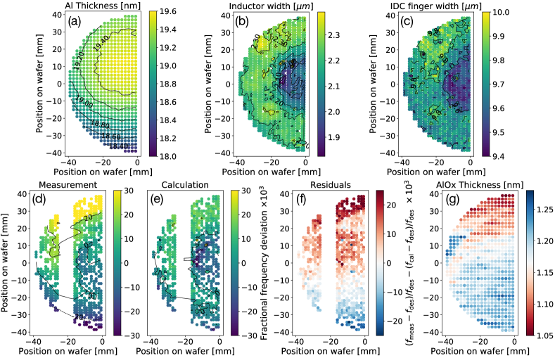
After fabrication, dicing and wire bonding, the array is cooled down to 100 mK in a dilution cryostat. Due to a limited number of connections in our test cryostat, only 4 out of 8 feedlines were connected. One feedline was found to be broken, the resulting measurements were performed on 3 feedlines with 920 designed resonators. Both S21 and mapping measurement were performed with the cryostat window open. To locate the position of the resonances on wafer, we performed an optical mapping on this array using a beam mapper Shu et al. (2018a, b). This mapper consists of a blackbody cooled down to 50 K, in front of which a moving 300 K metal ball acts as a source. The Teflon window of this mapper has a 20% emissivity at 300 K, which increases the total background radiation to the equivalent of a 110 K blackbody. The mapping was performed by scanning y-axis at fixed position. The step is 1 mm, corresponding to 0.4 mm on focal plane. We scan the metal ball at , corresponding to on focal plane. With a readout frequency of 23 Hz, this gives a position resolution of . Compared with the designed 1.4 mm pitch size between resonators, this configuration has enough accuracy to locate them individually. On each feedline, the resonators were measured simultaneously using a NIKEL readout board Bourrion et al. (2016). Fig. 1d shows the measured fractional resonance frequency deviation, defined as , where is the initially designed resonance frequency and is the measured resonance frequency.
To understand the cause of this frequency deviation, we calculated the frequency deviation through equation , with the magnetic inductance, the kinetic inductance, and the capacitance. From simulation using a commercial software package (Sonnet), we have nH with the designed inductor width , and with , where is the capacitance for each resonator with the designed IDC finger width and is the resonance frequency with . The kinetic inductance is given by , where mm is the inductor length. The thickness dependence of is non-trivial since both critical temperature and resistivity vary significantly with film thickness in our thickness range. We use an empirical relation pH/, with in nanometers, which is obtained from a series of independent measurements on sputter deposited films, while noting that this relation might not be perfectly adapted for our current e-beam evaporated film.
The geometry dimensions used in calculation are shown in Figure 1a-c. The aluminium film thickness was measured just after deposition, using ellipsometry. The thickness varies from 18.0 nm to 19.6 nm over the wafer, in a concentric fashion that is expected from thin film deposition using e-beam evaporation. The inductor width and IDC finger width are measured for each individual pixel using scanning electron microscopy (SEM). Both dimensions show a large variation, with notably a large size reduction in the center of the array. These variations are possibly due to variations in the photolithography process, like the variation in resist thickness, or variations in local wet etching speed, and are currently under investigation.
Using the calculation described above, we calculate the explained fractional frequency deviation, as shown in Fig. 1e. The residual, unexplained, frequency deviation is shown in Fig. 1f. The average residual frequency deviation is , with a standard deviation of (20 MHz). This is not sufficiently precise to predict resonance frequencies without an optical measurement. We note that the residuals are most significant in a small area in the upper left region of the wafer, which region is also observed in the results after trimming. Moreover, we find a strong correlation () between residual frequency deviation and aluminum oxide (AlOx) thickness (measured with ellipsometry before film processing, and shown in Fig. 1g) for the region where the residuals are , suggesting that the residuals are mainly related with . We have no means of measuring or other electrical film parameters locally, due to the dense packing of this telescope-class array.
In the optical mapping, the positions of 635 (69%) resonators were identified. For the unidentified resonators, we used radial basis functions to interpolate or extrapolate their resonance frequencies. We re-designed the resonance frequencies after trimming as , ranging from for each feedline. As both and use the same relation between IDC finger lengths and resonance frequencies, the corresponding trimming frequencies of the patterns on the trimming mask are given by , assuming the same frequency deviation
| (1) |
The final trimming mask is defined by the difference of the IDC patterns between and designs.
As described before Shu et al. (2018a), the trimming process consists of a contact lithography and Al wet-etching step. As the photoresist residue in small patterns can block wet-etching, an oxygen plasma was applied to remove the residue after development. During etching process, a large part of the backside 200 nm Al was etched away, so a new layer of 200 nm Al was sputtered on top of the Al residue.
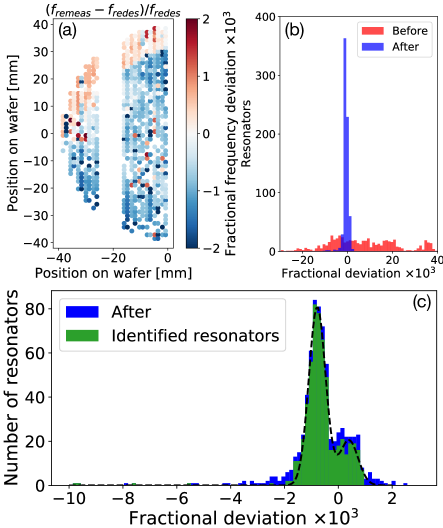
After trimming, the array was re-bonded and cooled down to 100 mK using the same setup as in the first characterization. S21 and mapping measurements are applied on the same three feedlines. The resonance frequencies after trimming range as the redesigned frequency . After trimming, the overall standard deviation of is , improved by a factor of 14. For the resonators identified beforehand, the standard deviation is is , indicating that the radial basis function used to inter/extrapolate the resonance frequencies works well on large format arrays. We also notice that trimming one or two pairs of IDC fingers give similar accuracy.
Fig. 2a shows two groups of resonators on the array, with a similar standard deviation of but different mean values. One group has , and its mean value of -1.7 MHz is consistent with previous trimming results Liu et al. (2017); Shu et al. (2018a), due to Al film aging. The other resonator group with , is located at the upper region of the array, partly overlapping with where the residuals . From the residual map (Fig. 1g) we know that this region has a lower compared with calculation, indicating a lower . However, this should not give two groups of if aging happens uniformly. This positive suggests that is either unchanged (no aging) or slightly increased, as should not decrease. By checking previous data, we confirm that this AlOx pattern was reproducible. One possible reason is nonuniformity of the argon plasma cleaning, just before the Al deposition, which creates a varying roughness of the substrate. Larger substrate roughness would facilitate film ageing.
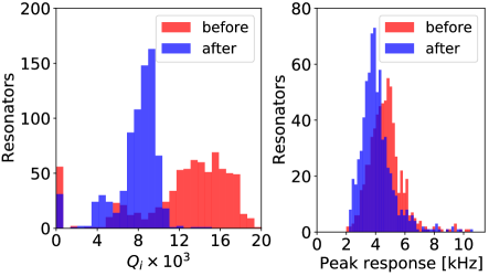
and are extracted from S21 measured using VNA under a 110 K background. After trimming, remains the same, while is decreased by from to . As using a K background radiation gives higher in both cases, here are limited by the 110 K background radiation. In a previous experiment, we observed an average dark of after trimming, much higher than the optical here. The film aging and the trimming process may have little effect on our , which is limited by the loss of quasiparticles created by photons. To compare the sensitivity, we directly take the peak response of the mapping source, shown in Fig. 3b, as the noise is dominated by the noise of the background temperature variation and the readout board. The peak response of the mapping source decreases from after trimming (Fig. 3), consistent with the 21% decrease of from to .
As the inductor geometry is untouched during trimming and the background temperature of the mapping system is stable, we can remove the influence of dimensions and incident power. The high trimming accuracy of suggests that the change of sheet resistance and gap energy of the Al film should also be at the same level, according to , which cannot explain the 40% degradation of . Using Mattis-Bardeen theory Mattis and Bardeen (1958), the equivalent temperatures corresponding to the observed are 334 mK and 361 mK before and after trimming, much larger than the 100 mK bath temperature, suggesting a small change in heat sinking may give this degradation of . The heat sinking of this array is determined by the contact between the backshort Al film and the Al sample holder. In a similar measurement, we observed that using an Al-Au bilayer as a backshort and a copper sample holder increased the from to under a 300 K optical loading. Because the backside Al is re-deposited, as described above, we suggest that the decrease of is due to a decrease in heat sinking. This could be remedied by using a Ti-Au bilayer backshort, which can trap phonons Karatsu et al. (2019), improve heat-sinking, and is resistant to Al etching process.
The yield of this array was measured under the 110 K blackbody radiation, a typical on-telescope condition. For reference, the on-telescope sky background radiation varies from 30 K to 180 K depending on the atmospheric opacity Perotto et al. (2020). After trimming, the yield is increased from 69% to 76% counted from optical mapping results. For all counted pixels, no crosstalk is observed from the 2-dimensional mapping results, with signal to noise ratio of 10. 45 resonators are missed by the readout system due to the limited number of readout tones. Including these missed resonators, the final yield is 81%, 10% higher than the on-telescope yield of the current NIKA2 260 GHz array Adam et al. (2018), while the initial fabrication yield is 84% for both arrays. The yield could be further increased by improving our fabrication process. resonances were broken during trimming process, giving the trimming fabrication yield of .
In conclusion, we have studied and minimized the resonance frequency deviations in a 4-inch kilo-pixel LEKID array. The calculation agrees with the measurement within an accuracy of . The decrease of the optical-loaded quality factor, after trimming, could be explained by a degradation of the heat sinking instead of a film property change. After trimming, the mapping yield, measured under a 110 K background, is improved from 69% to 76%, which can be further improved to 81% after updating our readout system. This improvement in yield within fixed readout bandwidth suggests that the trimming technique is capable to improve the on-telescope yield, which may benefit future large-format LEKID arrays.
See supplementary material for the design in detail.
The authors thank D. Billon-Pierron and A. Barbier for experimental help, and K.F. Schuster for useful discussions. This work has been partially funded by LabEx FOCUS ANR-1-LABX-0013.
Data availability
The data that support the findings of this study are available from the corresponding author upon reasonable request.
References
- Day et al. (2003) P. K. Day, H. G. LeDuc, B. A. Mazin, A. Vayonakis, and J. Zmuidzinas, Nature 425, 817 (2003).
- Doyle et al. (2008) S. Doyle, P. Mauskopf, J. Naylon, A. Porch, and C. Duncombe, Journal of Low Temperature Physics 151, 530 (2008).
- Adam et al. (2018) R. Adam, A. Adane, P. Ade, P. André, A. Andrianasolo, H. Aussel, A. Beelen, A. Benoit, A. Bideaud, N. Billot, et al., Astronomy & Astrophysics 609, A115 (2018).
- Wandui et al. (2020) A. Wandui, J. J. Bock, C. Frez, M. Hollister, L. Minutolo, H. Nguyen, B. Steinbach, A. Turner, J. Zmuidzinas, and R. O’Brient, Journal of Applied Physics 128, 044508 (2020).
- Austermann et al. (2018) J. Austermann, J. Beall, S. Bryan, B. Dober, J. Gao, G. Hilton, J. Hubmayr, P. Mauskopf, C. McKenney, S. Simon, et al., Journal of Low Temperature Physics 193, 120 (2018).
- Wheeler et al. (2018) J. Wheeler, S. Hailey-Dunsheath, E. Shirokoff, P. Barry, C. Bradford, S. Chapman, G. Che, S. Doyle, J. Glenn, S. Gordon, et al., Journal of Low Temperature Physics 193, 408 (2018).
- Walter et al. (2020) A. B. Walter, N. Fruitwala, S. Steiger, J. I. Bailey III, N. Zobrist, N. Swimmer, I. Lipartito, J. P. Smith, S. R. Meeker, C. Bockstiegel, et al., Publications of the Astronomical Society of the Pacific 132, 125005 (2020).
- Mazin (2020) B. A. Mazin, “Superconducting materials for microwave kinetic inductance detectors,” (2020), arXiv:2004.14576 [astro-ph.IM] .
- Liu et al. (2017) X. Liu, W. Guo, Y. Wang, M. Dai, L. Wei, B. Dober, C. McKenney, G. Hilton, J. Hubmayr, J. Austermann, et al., Applied Physics Letters 111, 252601 (2017).
- Shu et al. (2018a) S. Shu, M. Calvo, J. Goupy, S. Leclercq, A. Catalano, A. Bideaud, A. Monfardini, and E. F. Driessen, Applied Physics Letters 113, 082603 (2018a).
- Calvo et al. (2016) M. Calvo, A. Benoît, A. Catalano, J. Goupy, A. Monfardini, N. Ponthieu, E. Barria, G. Bres, M. Grollier, G. Garde, J. P. Leggeri, G. Pont, S. Triqueneaux, R. Adam, O. Bourrion, J. F. Macías-Pérez, M. Rebolo, J. P. Scordilis, D. Tourres, A. Adane, G. Coiffard, S. Leclercq, F. X. Désert, S. Doyle, P. Mauskopf, C. Tucker, P. Ade, P. André, A. Beelen, B. Belier, A. Bideaud, N. Billot, B. Comis, A. D’Addabbo, C. Kramer, J. Martino, F. Mayet, F. Pajot, E. Pascale, L. Perotto, V. Revéret, A. Ritacco, L. Rodriguez, G. Savini, K. Schuster, A. Sievers, and R. Zylka, Journal of Low Temperature Physics 184, 816 (2016).
- Shu et al. (2018b) S. Shu, M. Calvo, S. Leclercq, J. Goupy, A. Monfardini, and E. Driessen, Journal of Low Temperature Physics 193, 141 (2018b).
- Bourrion et al. (2016) O. Bourrion, A. Benoit, J. Bouly, J. Bouvier, G. Bosson, M. Calvo, A. Catalano, J. Goupy, C. Li, J. Macías-Pérez, et al., Journal of Instrumentation 11, P11001 (2016).
- Mattis and Bardeen (1958) D. C. Mattis and J. Bardeen, Physical Review 111, 412 (1958).
- Karatsu et al. (2019) K. Karatsu, A. Endo, J. Bueno, P. de Visser, R. Barends, D. Thoen, V. Murugesan, N. Tomita, and J. Baselmans, Applied Physics Letters 114, 032601 (2019).
- Perotto et al. (2020) L. Perotto, N. Ponthieu, J. Macías-Pérez, R. Adam, P. Ade, P. André, A. Andrianasolo, H. Aussel, A. Beelen, A. Benoît, et al., Astronomy & Astrophysics 637, A71 (2020).
I Supplementary material
I.1 Array design
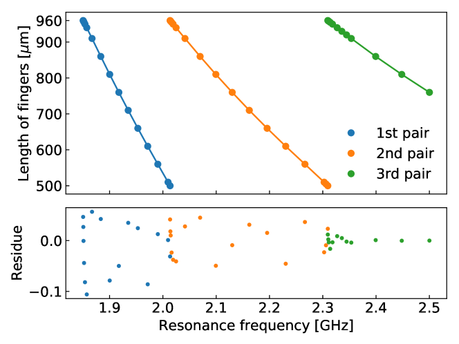
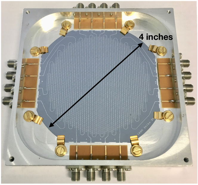
The whole focal plane of the NIKA2 instrument is a 80 mm diameter circle. With inductor size of 1 mm, in total there are 2392 resonators on 8 microstrip feedlines. The pitch size is optimized to be 1.4 mm. The single pixel design is shown in Fig. 4 in detail. Resonance frequencies are tune by shortening the length of IDC fingers pair by pair. The longest finger length is and the shortest length is . The resonance frequencies are simulated in Sonnet software with several different IDC finger lengths. A polynomial fit is applied to extracted the relation between finger length and resonance frequencies, shown in Fig. 5. The fitting residue is smaller than . In terms of resonance frequency, this corresponds to 5 kHz, much smaller than the simulated kHz electrical crosstalk. The resonance frequency after trimming is also defined in this way, so no extra simulations are needed for the re-designed resonance frequencies. The full array after fabrication is shown in Fig. 6.
