Mapping the phase diagram of a YBa2Cu3O7-δ nanowire through electromigration
Abstract
We use electromigration (EM) to tune the oxygen content of YBa2Cu3O7-δ (YBCO) nanowires. During EM, the dopant oxygen atoms in the nanowire are moved under the combined effect of electrostatic force and Joule heating. The EM current can be tuned to either deplete or replenish nanowires with oxygen, allowing fine tuning of its hole doping level. Electrical transport measurements and Kelvin probe microscopy corroborate good homogeneity of the doping level along the electromigrated nanowires. Thus, EM provides an effective method to study transport properties of YBCO in a wide doping range at the nanoscale in one and the same device.
I Introduction
The discovery of copper oxide-based High-critical Temperature Superconductors (HTSs), more than 30 years ago, ranks among the major scientific events in solid state physics and has given a tremendous boost to the field of superconductivity. The strong electron-electron correlations of these compounds lead to a plethora of symmetry breaking orders, such as charge and spin density waves, which strongly depend on the doping level of these materials [1]. The rather similar energy scales of those orders result in an intertwined ground state where charge, spin, lattice, and orbital degrees of freedom are entangled in a complex manner leading to an intricate temperature-doping phase diagram. The least understood phase, the so-called strange metal phase, is characterized by a linear-in- resistivity at temperatures above the pseudogap temperature. This phase is suggested to originate from a putative quantum critical point close to optimal doping [2, 3], which possibly promotes superconductivity in these materials. The study of HTSs in the form of nanowires [4, 5, 6, 7] and nanodots [8] at various doping levels is expected to shine light on the microscopic mechanism leading to superconductivity in these materials, which emerges from such a complex ground state below the superconducting transition temperature . Here, investigating transport properties on length scales comparable to correlation length scales of various symmetry breaking orders will be instrumental to understand the interplay or intertwining between those orders and superconductivity [9, 10, 11, 12, 13]. At the same time nanoscale HTSs allow for the development of quantum limited sensors, such as nanoscale superconducting quantum interference devices [14, 15, 16, 17, 18, 19, 20, 21] and photon detectors [22, 23, 24, 25, 26, 27], whose properties can be strongly modified by changing the doping level.
Typically, nanowires with different doping levels are obtained by nanopatterning of thin films having the corresponding doping level, i.e. oxygen content, in the case of YBa2Cu3O7-δ (YBCO) [27, 23]. However, such a fabrication process is very challenging, especially for lower doping levels, and requires a separate YBCO film for each doping level [27]. Moreover, this approach makes the comparison between transport properties of nanowires of different doping levels difficult since properties such as critical current sensitively depend on wire morphology on the nanoscale [28], which will unavoidably vary between devices.
Tuning the doping of YBCO ex-situ would solve the limitations inherent to fabrication. One way to tune the material’s electrical properties is via electric field effect or gating. Although moderate success has been achieved, most gating techniques require either the use of ferroelectric materials [29, 30] or electrolytes [31], in combination with strong electric fields. Moreover, the effectiveness of gating is tied to the thickness of the material and limits its application to ultrathin films [32].
Another promising route to modify the doping level in one and the same structure is to use electromigration (EM) [33, 34]. Here the dopant oxygen atoms are moved by subjecting the material to large current densities in the normal state, thus tuning the doping level ex-situ. YBCO is a particularly good candidate for EM due to the low activation energy of the dopant oxygen atoms [35]. However, electromigration on m wide structures still suffer from rather inhomogeneous doping distributions along YBCO bridges [36].
In this work we use EM to tune the doping level of YBCO nanowires. We find that the doping can be increased or decreased depending on the waveform of the applied bias current. By applying a DC current we can replenish the oxygen in the nanostructures, while an AC current can be used to deplete it. The effect of the EM is studied by measuring the resistance versus temperature of the nanowires before and after the process. The resulting curves generally show a single sharp superconductive transition, which indicates homogeneity of the doping distribution. Successive steps of EM on a single nanowire are used to recreate most of the phase diagram of YBCO, covering a wide range of doping. Finally, Kelvin Probe Force Microscopy (KPFM) preformed on nanowires after EM confirms the homogeneous doping distribution along the wire.
II Results
The quality of the pristine YBCO nanowires is of paramount importance since defects are affected by the electromigration process and may worsen the quality of the nanowire with each EM step. The YBCO nanowires used in this work have been fabricated from thin films (close to the optimal doping) with thickness of nm. The thin films were first deposited by pulsed laser deposition (PLD) onto (110) oriented MgO substrates, and then covered by a hard layer of carbon, also deposited by PLD. Electron beam lithography and oxygen plasma etching are used to define the carbon mask, which is then used to etch the thin films in the final shape of the nanowires through Ar ion milling. Finally, the carbon mask is removed by oxygen plasma etching. This fabrication has been shown to yield high quality nanowires, both for optimally- [37, 38, 39] and under-doped [27] films.
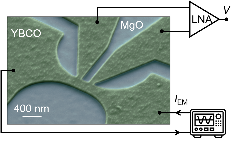
A scanning electron microscope (SEM) image of a nanowire is shown in Fig. 1. The nanowires are patterned with a 4-point geometry, with nm width and nm length (distance between voltage probes). We use rounded inner corners at the end points of the nanowires to mitigate the effect of current crowding [40, 41, 28], which could locally increase the effect of the EM process. In Fig. 1 is also reported the schematic of the electromigration and measurement setup connected to the nanowire. An arbitrary waveform generator (AWG) is connected to the nanowire and supplies the EM current, while the voltage drop along the nanowire is amplified by a low noise amplifier (LNA).
The electromigration is typically performed at room temperature, although it can be done also at lower temperature, , without significant changes. We perform two types of electromigration: DC-EM, where the AWG is maintained at a DC bias value during the whole process, and AC-EM, where the AWG output is an ambipolar square wave signal, i.e. a pulse train. These two types of EM waveforms have different effects on the nanowire doping as will be discussed below.
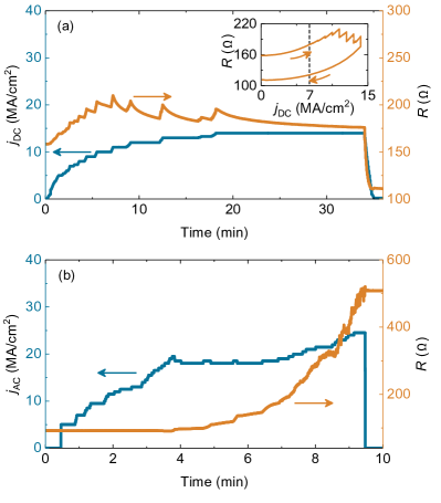
An example of DC-EM is shown in Fig. 2(a). We start with a nearly optimally doped nanowire with hole doping and resistance . Here the doping level is estimated by comparing the superconducting transition temperature of the nanowire to that of YBCO films of known hole doping [42]. The DC bias current density across the wire, , is manually increased while is monitored. For low values of ( MA/cm2) the resistance increases approximately quadratically with the current density, see inset of Fig. 2 (a). This behavior is caused by the local temperature increase in the wire , due to Joule heating, and the linear in resistance of optimally doped YBCO.
The bias current is further increased until it is sufficiently high to start the EM of the dopant oxygen atoms, which happens for MA/cm2. In this regime, with kept constant, the nanowire resistance slowly decreases over time. A reduction in indicates that the doping level of the nanowire is increased [42] and oxygen is being replenished in the nanostructure. Once is increased even further, starts decreasing faster (see Fig. 2(a)). After the DC-EM, i.e. when is brought back to , the nanowire resistance drops to . From this value and the superconducting transition temperature (data not shown) we estimate that the doping level inside the wire has increased to a value [42].
However, the bias current used for DC-EM cannot be increased indefinitely. We observe that if is raised above a certain threshold ( MA/cm2), the DC-EM causes a depletion of the oxygen atoms within the wire. This means that at high bias, DC-EM lowers the nanowire doping instead of increasing it. Moreover, when the oxygen is reduced by DC-EM, the resulting nanowires show inhomogeneous transport properties, e.g. multiple superconducting transitions (data not shown). Therefore, in this work DC-EM is only used for increasing the doping of YBCO nanowires.
To achieve homogeneous reduction of the doping level one can instead use AC-EM, which results in a controlled depletion of oxygen in the nanowires. The bias current waveform used for AC-EM is a square wavefunction centered around zero, with peak to peak current density and frequency kHz. At this frequency the effect of electromigration is negligible due to the relatively long oxygen diffusion relaxation times [43]. Instead, thermomigration of oxygen atoms due to large temperature gradients between the wire and the electrodes dominates the oxygen migration process in YBCO nanowires [44]. Here, similar to the DC-EM, the resistance of the nanowire is measured between 100 ms long AC-EM bursts to monitor the effect of the electromigration. An example of AC-EM is shown in Fig. 2(b). Here we start with a nanowire with and . When is sufficiently high ( MA/cm2), starts to increase. Increasing further causes a faster increase of the wire resistance . During AC-EM, needs to be increased slowly to avoid thermal runaway related to the abrupt increase of , which would be detrimental for the nanowire. In Fig. 2(b) the bias current is adjusted multiple times during the EM to avoid thermal runaway. After the AC-EM process, the nanowire resistance has increased to corresponding to a reduction of the doping value to (determined from of the resistive transition [42]).
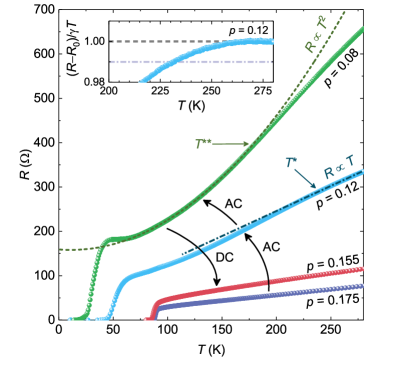
In Fig. 3 we show four measurements of resistance versus temperature, , done on the same nanowire to compare the effect of DC- and AC-EM. Starting from a slightly overdoped nanowire, , we apply first AC-EM to lower the doping to , and a second time to further lower the nanowire doping to . The decrease in doping results in an increase of the resistance, and a lower critical temperature K. DC-EM is then used to increase the nanowire doping up to , i.e. in the optimally doped regime of YBCO. Higher is accompanied by higher K and lower value of resistance. It is important to note that the curves after EM (both AC and DC) present a single superconductive transition, which indicates homogeneity of the doping along the nanowire. Thus, a combination of DC- and AC-EM can be used to increase or to decrease the doping of our nanowires, respectively, and therefore fine tune the doping level.
| doping | [K] | [K] | [K] | |
|---|---|---|---|---|
| nanowire | 0.155 | 148 | - | 4.5 |
| film | 0.155 | 145 | - | 3.4 |
| nanowire | 0.12 | 230 | 120 | 14 |
| film | 0.12 | 215 | 118 | 6 |
| nanowire | 0.08 | 271 | 170 | 14 |
| film | 0.08 | 263 | 170 | 7 |
To confirm the homogeneity of the nanowires we can first extract the superconducting transition width, , which is defined as the temperature range in which the wire resistance changes from to of the normal state resistance [42]. The values of extracted for our nanowires are reported in Table 1, with the values obtained in thin films at similar doping. Only when we reach the strongly underdoped regime, the superconducting transitions of the nanowires become wider in than for the thin films.
Of particular interest are the various characteristic temperatures, which can be extracted from the curve of a YBCO nanowire. These temperatures can be compared to those extracted from YBCO thin films [42] to further asses the quality of our nanowires after electromigration. Here we focus on two characteristic temperatures, the first is , i.e. the temperature below which the departs from linearity (), as indicated in Fig. 3 for . The second characteristic temperature is , i.e. the upper bound of the range in which , as shown in Fig. 3 for . In the inset of Fig. 3 we show the relative deviation of the measured at from the linear in dependence. The value of is determined as the temperature below which the departs by more than from the linear-in- dependence, indicated in the inset by the dash-dotted line.
In Table 1 the values of , and extracted from the curves from Fig. 3 are compared to the values reported for YBCO thin films at similar doping [42]. Indeed, from this table one can see only small variations between the thin-film and our nanowire properties. After the electromigration, the nanowire properties are therefore still close to pristine YBCO films. Such occurrence highlights that the effects of the electromigration are limited to the displacement of oxygen atoms, without degradation of the underlying material, resulting in homogeneous YBCO nanowires in a broad doping range.
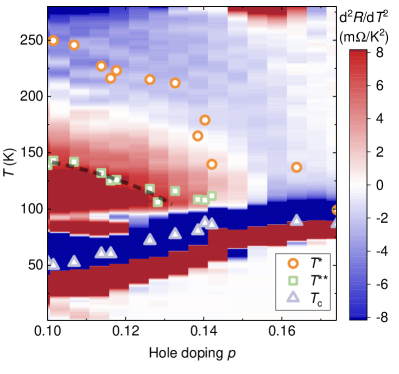
By performing AC-EM on a single nanowire we reproduced the phase diagram of YBCO shown in Fig. 4. The nanowire was fabricated with with . Its doping was reduced in successive steps of AC-EM, while the was measured after each step. In Fig. 4 we show the second derivative of the measured resistance versus temperature, , as a function of temperature and doping. This phase diagram is in good agreement with the one obtained from YBCO thin films [42] and bulk samples [45, 46]. One can clearly identify the linear in resistivity behavior in the strange metal phase slightly above the optimal doping level (see white colored region for and in Fig. 4).
Moreover, for comparison, the values of , and extracted from measurements performed on YBCO thin films [42] have been added to Fig. 4 (open symbols). The values of extracted from the curves of our nanowires lie close to the thin films values (orange circles). However, the phase diagram shows that the white region, which corresponds to purely linear , is well above these values. A similar behavior has been reported for bulk crystals [45]. Overall, we find a good agreement between our phase diagram and the one reported in literature for bulk crystals [45], confirming that EM can be used for tuning ex-situ the doping of individual YBCO nanowires while preserving electrical properties close to those of pristine thin films and single crystals.
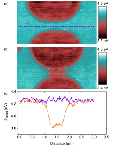
To further investigate the local effect of EM on the nanowires, we employ Kelvin probe force microscopy (KPFM) to visualize the doping distribution after EM with nanometer resolution. KPFM is a variant of non-contact atomic force microscopy (AFM), which measures the difference in work function, , between the nanowire surface and the conductive AFM tip [47].
Two nanowires, one slightly overdoped (as-fabricated, ) and one underdoped (, obtained through AC-EM), have been imaged. In order to obtain absolute values of the work function in YBCO, , we have performed a calibration of the AFM tip work function, , using a highly oriented pyrolytic graphite sample (HOPG): , where is the measured potential difference between the AFM tip and the HOPG surface, and eV is the work function of HOPG. The work function of the YBCO nanowire can then be obtained as , where is the measured surface potential difference between the tip and the YBCO nanowire. The measured KPFM maps of of the YBCO nanowire before and after EM treatment are shown in Fig. 5. The absolute value of eV is close to values reported earlier for optimally doped YBCO bulk polycrystalline [48] and thin film [49] samples. In the EM-treated underdoped YBCO nanowire, the central region has significantly lower work function as compared with the wide electrodes. The value of the work function taken along the nanowire, i.e. along the linecuts in panel (a) and (b), are shown in panel (c). The difference in work function is about V between the slightly overdoped and underdoped YBCO nanowires.
The work function is defined as a difference between the Fermi level of a metal and vacuum level just outside the surface. Thus the work function of YBCO, , and cuprates in general, is expected to be influenced by the doping, and by measuring the work function one can indirectly map the doping distribution in our nanowires. Indeed, the difference between work functions of optimally doped and underdoped YBCO nanowires is in good agreement with the chemical potential shift as a function of doping measured by X-ray photoemission spectroscopy [50, 51]. On the other hand, KPFM is a surface sensitive technique and the potential difference may also depend on a surface dipole layer due to the presence of adsorbates. A similar change in work function was found in YBCO films modified using scanning tunneling microscopy [52]. The result was interpreted as due to the presence of trapped charges at the oxygen vacancies at the modified surface. While we cannot rule out that similar effects contribute to the difference in work function in our nanowires, we emphasize that the transport properties indicate that the modification occurs in the bulk of the YBCO rather than at the surface.
III Conclusions
We have presented an electromigration technique which can be used to fine tune the oxygen content, and thus the doping level, of YBCO nanowires. Depending on the bias current waveform used for the EM we can increase (DC-EM) or decrease (AC-EM) the nanowire doping. We used EM to reproduce most of the phase diagram of YBCO with a single nanowire. We used KPFM imaging to asses the effect of the EM on the morphology and work function of the nanowires after EM. This confirmed that the doping distribution in electromigrated nanowires is homogeneous over a consistent area. The ex-situ control of the doping level in YBCO nanowires is a milestone towards an in-depth study of the phase diagram of cuprates on the nanoscale and opens the way to investigate transport properties in the proximity of putative quantum critical points [1] in one and the same nanowire where fine tuning of the doping level is required. Moreover, this technique is interesting for the technological applications of YBCO weak links, where the tuning of the nanowire properties, such as critical current and kinetic inductance, is required.
Acknowledgements.
This work has been performed in part at Myfab Chalmers and is supported by the Knut and Alice Wallenberg Foundation (KAW) under the project “NeuroSQUID” (2014.0102_KAW) and the Swedish Research Council (2020-05184_VR, 2018-04658_VR, 2020-04945_VR).References
- Keimer et al. [2015] B. Keimer, S. A. Kivelson, M. R. Norman, S. Uchida, and J. Zaanen, From quantum matter to high-temperature superconductivity in copper oxides, Nature 518, 179 (2015).
- Ramshaw et al. [2015] B. Ramshaw, S. Sebastian, R. McDonald, J. Day, B. Tan, Z. Zhu, J. Betts, R. Liang, D. Bonn, W. Hardy, et al., Quasiparticle mass enhancement approaching optimal doping in a high-tc superconductor, Science 348, 317 (2015).
- Varma [2020] C. M. Varma, Colloquium: Linear in temperature resistivity and associated mysteries including high temperature superconductivity, Rev. Mod. Phys. 92, 031001 (2020).
- Lombardi et al. [1998] F. Lombardi, Z. Ivanov, G. Fischer, E. Olsson, and T. Claeson, Transport and structural properties of the top and bottom grain boundaries in yba 2 cu 3 o 7- step-edge josephson junctions, Appl. Phys. Lett. 72, 249 (1998).
- Mohanty et al. [2004] P. Mohanty, J. Wei, V. Ananth, P. Morales, and W. Skocpol, Nanoscale high-temperature superconductivity, Physica C 408, 666 (2004).
- Bonetti et al. [2004] J. Bonetti, D. Caplan, D. J. Van Harlingen, and M. Weissman, Electronic transport in underdoped yba2cu3o7-δ nanowires: evidence for fluctuating domain structures, Phys. Rev. Lett. 93, 087002 (2004).
- Carillo et al. [2010] F. Carillo, G. Papari, D. Stornaiuolo, D. Born, D. Montemurro, P. Pingue, F. Beltram, and F. Tafuri, Little-parks effect in single nanoscale yba 2 cu 3 o 6+ x rings, Phys. Rev. B 81, 054505 (2010).
- Gustafsson et al. [2013] D. Gustafsson, D. Golubev, M. Fogelström, T. Claeson, S. Kubatkin, T. Bauch, and F. Lombardi, Fully gapped superconductivity in a nanometre-size yba2cu3o7-δ island enhanced by a magnetic field, Nat. Nanotechnol. 8, 25 (2013).
- Fradkin et al. [2015] E. Fradkin, S. A. Kivelson, and J. M. Tranquada, Colloquium: Theory of intertwined orders in high temperature superconductors, Rev. Mod. Phys. 87, 457 (2015).
- Auvray et al. [2019] N. Auvray, B. Loret, S. Benhabib, M. Cazayous, R. Zhong, J. Schneeloch, G. Gu, A. Forget, D. Colson, I. Paul, et al., Nematic fluctuations in the cuprate superconductor bi 2 sr 2 cacu 2 o 8+ , Nat. Commun. 10, 1 (2019).
- Loret et al. [2019] B. Loret, N. Auvray, Y. Gallais, M. Cazayous, A. Forget, D. Colson, M.-H. Julien, I. Paul, M. Civelli, and A. Sacuto, Intimate link between charge density wave, pseudogap and superconducting energy scales in cuprates, Nat. Phys. 15, 771 (2019).
- Wahlberg et al. [2021] E. Wahlberg, R. Arpaia, G. Seibold, M. Rossi, R. Fumagalli, E. Trabaldo, N. B. Brookes, L. Braicovich, S. Caprara, U. Gran, et al., Restored strange metal phase through suppression of charge density waves in underdoped yba2cu3o7-, Science 373, 1506 (2021).
- Huang et al. [2021] H. Huang, S.-J. Lee, Y. Ikeda, T. Taniguchi, M. Takahama, C.-C. Kao, M. Fujita, and J.-S. Lee, Two-dimensional superconducting fluctuations associated with charge-density-wave stripes in la 1.87 sr 0.13 cu 0.99 fe 0.01 o 4, Phys. Rev. Lett. 126, 167001 (2021).
- Arpaia et al. [2014] R. Arpaia, M. Arzeo, S. Nawaz, S. Charpentier, F. Lombardi, and T. Bauch, Ultra low noise yba2cu3o7-δ nano superconducting quantum interference devices implementing nanowires, Appl. Phys. Lett. 104, 072603 (2014).
- Schwarz et al. [2015] T. Schwarz, R. Wölbing, C. F. Reiche, B. Müller, M.-J. Martínez-Pérez, T. Mühl, B. Büchner, R. Kleiner, and D. Koelle, Low-noise yba 2 cu 3 o 7 nano-squids for performing magnetization-reversal measurements on magnetic nanoparticles, Phys. Rev. Applied 3, 044011 (2015).
- Charpentier et al. [2016] S. Charpentier, R. Arpaia, J. Gaudet, D. Matte, R. Baghdadi, T. Löfwander, D. Golubev, P. Fournier, T. Bauch, and F. Lombardi, Hot spot formation in electron-doped pcco nanobridges, Phys. Rev. B 94, 060503 (2016).
- Arzeo et al. [2016] M. Arzeo, R. Arpaia, R. Baghdadi, F. Lombardi, and T. Bauch, Toward ultra high magnetic field sensitivity yba2cu3o7-δ nanowire based superconducting quantum interference devices, J. Appl. Phys. 119, 174501 (2016).
- Martínez-Pérez et al. [2018] M. Martínez-Pérez, J. Pablo-Navarro, B. Muller, R. Kleiner, C. Magén, D. Koelle, J. De Teresa, and J. Sesé, Nanosquid magnetometry on individual as-grown and annealed co nanowires at variable temperature, Nano Letters 18, 7674 (2018).
- Trabaldo et al. [2019] E. Trabaldo, C. Pfeiffer, E. Andersson, R. Arpaia, A. Kalaboukhov, D. Winkler, F. Lombardi, and T. Bauch, Grooved dayem nanobridges as building blocks of high-performance yba2cu3o7-δ squid magnetometers, Nano Lett. 19, 1902 (2019).
- Li et al. [2020] H. Li, H. Cai, E. Y. Cho, S. J. McCoy, Y.-T. Wang, J. C. LeFebvre, Y. W. Zhou, and S. A. Cybart, High-transition-temperature nanoscale superconducting quantum interference devices directly written with a focused helium ion beam, Appl. Phys. Lett. 116, 070601 (2020).
- Trabaldo et al. [2020] E. Trabaldo, S. Ruffieux, E. Andersson, R. Arpaia, D. Montemurro, J. Schneiderman, A. Kalaboukhov, D. Winkler, F. Lombardi, and T. Bauch, Properties of grooved dayem bridge based yba2cu3o7-δ superconducting quantum interference devices and magnetometers, Appl. Phys. Lett. 116, 132601 (2020).
- Curtz et al. [2010] N. Curtz, E. Koller, H. Zbinden, M. Decroux, L. Antognazza, Ø. Fischer, and N. Gisin, Patterning of ultrathin ybco nanowires using a new focused-ion-beam process, Supercond. Sci. Technol. 23, 045015 (2010).
- Arpaia et al. [2017] R. Arpaia, D. Golubev, R. Baghdadi, R. Ciancio, G. Dražić, P. Orgiani, D. Montemurro, T. Bauch, and F. Lombardi, Transport properties of ultrathin yba2cu3o7-δ nanowires: A route to single-photon detection, Phys. Rev. B 96, 064525 (2017).
- Shibata et al. [2017] H. Shibata, N. Kirigane, K. Fukao, D. Sakai, S. Karimoto, and H. Yamamoto, Photoresponse of a la1. 85sr0. 15cuo4 nanostrip, Supercond. Sci. Technol. 30, 074001 (2017).
- Ejrnaes et al. [2017] M. Ejrnaes, L. Parlato, R. Arpaia, T. Bauch, F. Lombardi, R. Cristiano, F. Tafuri, and G. Pepe, Observation of dark pulses in 10 nm thick ybco nanostrips presenting hysteretic current voltage characteristics, Supercond. Sci. Technol. 30, 12LT02 (2017).
- Amari et al. [2017] P. Amari, C. Feuillet-Palma, A. Jouan, F. Couëdo, N. Bourlet, E. Géron, M. Malnou, L. Méchin, A. Sharafiev, J. Lesueur, et al., High-temperature superconducting nano-meanders made by ion irradiation, Supercond. Sci. Technol. 31, 015019 (2017).
- Andersson et al. [2020] E. Andersson, R. Arpaia, E. Trabaldo, T. Bauch, and F. Lombardi, Fabrication and electrical transport characterization of high quality underdoped yba2cu3o7-δ nanowires, Supercond. Sci. Technol. 33, 064002 (2020).
- Nawaz et al. [2013a] S. Nawaz, R. Arpaia, F. Lombardi, and T. Bauch, Microwave response of superconducting yba2cu3o7-δ nanowire bridges sustaining the critical depairing current: Evidence of josephson-like behavior, Phys. Rev. Lett. 110, 167004 (2013a).
- Lemanov et al. [1993] V. Lemanov, A. Kholkin, and A. Sherman, Ybco thin films on ferroelectric substrates: the polarization-induced changes of superconductive properties, Supercond. Sci. Technol. 6, 814 (1993).
- Crassous et al. [2013] A. Crassous, R. Bernard, S. Fusil, K. Bouzehouane, J. Briatico, M. Bibes, A. Barthélémy, and J. E. Villegas, Bifeo3/yba2cu3o7-δ heterostructures for strong ferroelectric modulation of superconductivity, J. Appl. Phys. 113, 024910 (2013).
- Zhang et al. [2017] L. Zhang, S. Zeng, X. Yin, T. C. Asmara, P. Yang, K. Han, Y. Cao, W. Zhou, D. Wan, C. S. Tang, et al., The mechanism of electrolyte gating on high-tc cuprates: The role of oxygen migration and electrostatics, ACS Nano 11, 9950 (2017).
- Xi et al. [1991] X. Xi, Q. Li, C. Doughty, C. Kwon, S. Bhattacharya, A. Findikoglu, and T. Venkatesan, Electric field effect in high tc superconducting ultrathin yba2cu3o7-x films, Appl. Phys. Lett. 59, 3470 (1991).
- Moeckly et al. [1993] B. Moeckly, D. Lathrop, and R. Buhrman, Electromigration study of oxygen disorder and grain-boundary effects in yba 2 cu 3 o 7- thin films, Phys. Rev. B 47, 400 (1993).
- Baumans et al. [2019] X. D. Baumans, A. Fernández-Rodríguez, N. Mestres, S. Collienne, J. Van de Vondel, A. Palau, and A. V. Silhanek, Electromigration in the dissipative state of high-temperature superconducting bridges, Appl. Phys. Lett. 114, 012601 (2019).
- Scouten et al. [1994] S. Scouten, Y. Xu, B. Moeckly, and R. Buhrman, Low-frequency noise in the normal state of thin-film high-temperature superconductors, Phys. Rev. B 50, 16121 (1994).
- Marinković et al. [2020] S. Marinković, A. Fernández-Rodríguez, S. Collienne, S. B. Alvarez, S. Melinte, B. Maiorov, G. Rius, X. Granados, N. Mestres, A. Palau, and A. V. Silhanek, Direct visualization of current-stimulated oxygen migration in YBa2Cu3O7-δ thin films, ACS Nano 14, 11765 (2020).
- Nawaz et al. [2013b] S. Nawaz, R. Arpaia, T. Bauch, and F. Lombardi, Approaching the theoretical depairing current in yba2cu3o7-x nanowires, Physica C 495, 33 (2013b).
- Arpaia et al. [2016] R. Arpaia, M. Arzeo, R. Baghdadi, E. Trabaldo, F. Lombardi, and T. Bauch, Improved noise performance of ultrathin ybco dayem bridge nanosquids, Supercond. Sci. Technol. 30, 014008 (2016).
- Trabaldo et al. [2017] E. Trabaldo, M. Arzeo, R. Arpaia, R. Baghdadi, E. Andersson, F. Lombardi, and T. Bauch, Noise properties of ybco nanostructures, IEEE Trans. Appl. Supercond. 27, 7500904 (2017).
- Hagedorn and Hall [1963] F. B. Hagedorn and P. Hall, Right-angle bends in thin strip conductors, J. Appl. Phys. 34, 128 (1963).
- Clem and Berggren [2011] J. R. Clem and K. K. Berggren, Geometry-dependent critical currents in superconducting nanocircuits, Physical Review B 84, 174510 (2011).
- Arpaia et al. [2018] R. Arpaia, E. Andersson, E. Trabaldo, T. Bauch, and F. Lombardi, Probing the phase diagram of cuprates with yba2cu3o7-δ thin films and nanowires, Phys. Rev. Materials 2, 024804 (2018).
- [43] An estimation of the diffusion relaxation time results in s, with diffusion constant [33] and wire length nm, considering an elevated temperature of K due to Joule heating.
- Oriani [1969] R. Oriani, Thermomigration in solid metals, Journal of Physics and Chemistry of Solids 30, 339 (1969).
- Ando et al. [2004] Y. Ando, S. Komiya, K. Segawa, S. Ono, and Y. Kurita, Electronic phase diagram of high-t c cuprate superconductors from a mapping of the in-plane resistivity curvature, Phys. Rev. Lett. 93, 267001 (2004).
- Barišić et al. [2013] N. Barišić, M. K. Chan, Y. Li, G. Yu, X. Zhao, M. Dressel, A. Smontara, and M. Greven, Universal sheet resistance and revised phase diagram of the cuprate high-temperature superconductors, Proceedings of the National Academy of Sciences 110, 12235 (2013).
- Melitz et al. [2011] W. Melitz, J. Shen, A. C. Kummel, and S. Lee, Kelvin probe force microscopy and its application, Surf. Sci. Rep. 66, 1 (2011).
- Koshida and Saito [1990] N. Koshida and K. Saito, Work function of a high-tc superconductor, yba2cu3o7, Jpn. J. Appl. Phys. 29, L1635 (1990).
- Rietveld et al. [1992] G. Rietveld, N. Y. Chen, and D. van der Marel, Anomalous temperature dependence of the work function in , Phys. Rev. Lett. 69, 2578 (1992).
- Maiti et al. [2009] K. Maiti, J. Fink, S. de Jong, M. Gorgoi, C. Lin, M. Raichle, V. Hinkov, M. Lambacher, A. Erb, and M. S. Golden, Doping dependence of the chemical potential and surface electronic structure in yba2cu3o6+x and la2-xsrxcuo4 using hard x-ray photoemission spectroscopy, Phys. Rev. B 80, 165132 (2009).
- Yagi et al. [2010] H. Yagi, T. Yoshida, A. Fujimori, K. Tanaka, N. Mannella, W. Yang, X. Zhou, D. Lu, Z.-X. Shen, Z. Hussain, et al., Characteristic electronic structure and its doping evolution in lightly-doped to underdoped yba2cu3oy, arXiv preprint arXiv:1002.0655 (2010).
- Urazhdin et al. [2003] S. Urazhdin, W. K. Neils, S. H. Tessmer, N. O. Birge, and D. J. V. Harlingen, Modifying the surface electronic properties of yba2cu3o7 with cryogenic scanning probe microscopy, Supercond. Sci. Technol. 17, 88 (2003).