Projected mushroom type phase-change memory
Keywords: Computational-memory, Projected phase-change memory, phase-change materials, Circuit Model, Nano-fabrication
Phase-change memory devices have found applications in in-memory computing where the physical attributes of these devices are exploited to compute in place without the need to shuttle data between memory and processing units. However, non-idealities such as temporal variations in the electrical resistance have a detrimental impact on the achievable computational precision. To address this, a promising approach is projecting the phase configuration of phase change material onto some stable element within the device. Here we investigate the projection mechanism in a prominent phase-change memory device architecture, namely mushroom-type phase-change memory. Using nanoscale projected Ge2Sb2Te5 devices we study the key attributes of state-dependent resistance, drift coefficients, and phase configurations, and using them reveal how these devices fundamentally work.
Phase change memory (PCM) devices can not only store data in their adjustable physical state but also use that data to perform computations by modifying an externally applied signal. This attribute has enabled their use in the emerging computational scheme of in-memory computingY2018zidanNatureElectronicsReview ; Y2018ielminiNatureElectronics ; Y2019mutluMandM ; Y2020AbuNatNano ; Y2018sebastianJAP ; Y2011kuzumNanoletters ; Y2018ielminiNatureElectronics ; Y2018yuProcIEEE . However, PCM in-memory computing continue to be based on more conventional architectures of PCMs, which were developed for binary data storageY2010Wong ; Y2011Xiong ; Y2016Arasu ; Y2017Ghazi and not computation. Important device non-idealities from the intrinsic material physics of phase-change materialsY2020ManuelJPD ; Y2009nardonePRB ; Y2016legalloESSDERC ; Y2010ielminiAPL ; Y2019carboniAEM ; Sebastian2019 ; Y2017GhaziMST thus arise and reduce the numerical precision achievable with this technology. Both materials and device engineering have been proposed as solutionsY2018LIunderstandingdrfit ; Y2019PCMHeterostructure ; y2013xiong ; Y2019thermalshen ; Y2021heterogeneouslyyang to minimizing these non-idealities. Device engineering invokes novel cell architectures, including the concept of projected PCMY2015koelmansNatComm ; Y2020BenediktScientificReports ; Y2013kimIEDM ; Y2016kimIEDM ; Y2010ProjectedLinerPatent . The concept decouples the readout characteristics of the device from the noisy electrical properties of the phase-change material. This is realized using an electrically conducting material, called the projection layer (liner) placed in parallel to the phase-change material. Thus, in effect, the device read-out characteristics become dictated by the properties of the projection layer.
The understanding of ‘projection’ has, however, remained limited to lateral-type architectures, which are not yet established for scaling-up. Of interest, therefore, are vertical devices with established materials and processing methods, that can be densely integrated and provide an optimized balance of key device properties, such as the mushroom-type PCM devicesY2021BOBBYIRPS ; Y2010Wong ; Y2010Burr ; Y2010PhaseChangeMemory ; Y2010ProjectedLinerPatent . In this article, we investigate the device characteristics of projected mushroom-type PCM (PMPCM) devices, and study the unique characteristics that distinguish them from their traditional unprojected counterparts. To that end, we construct an analytical model, and experimentally verify it using nanoscale devices projected to different extents. We specifically focus on the relevant properties of state-dependent resistance drift and temperature sensitivity, using which, we identify and discuss some guidelines for the device design of PMPCM.
Model of a projected mushroom-type PCM device
Figure 1A illustrates a sketch of a PMPCM device. The device consists of a layer of phase-change material sandwiched between a top (TE) and a narrower bottom (BE) electrode. Uniquely placed between the bottom electrode and the phase-change material is a thin film, which acts as the liner that spans the width and breadth of the device in dimensions. The resistance state of the device is dictated by the phase configuration, or the amount and geometry of amorphous volume (colored in red) in an otherwise crystalline phase-change material (colored in pink). A short, high current pulse (RESET), when applied to a device, amorphizes a fraction of the crystalline phase-change material in the region abutting the bottom electrode of radius . The amorphous volume brings the PCM device to a high-resistance state, where the resistance magnitude is dictated by the radius of this volume, which we refer to as . If one breaks down a PMPCM device in the RESET state into its lumped resistive components, it will comprise: (resistance to current from amorphous volume), (resistance from the remaining crystalline volume), (resistance from some shunt resistor), and (resistance from the liner). can further be broken into two resistors, namely and . is the resistance presented by the liner to the current that flows perpendicularly through it (this can be seen as the current that flows perpendicular to ), and is the resistance presented by the liner to the current that flows into it (this can be seen as the current that flows parallels to ). If an approximation is then made for the amorphous volume to have shape of a hemispherical dome, and the liner as a cylindrical discY2009Bipin ; Y1967Holm ; Y2010AbuAPL (see Figure 1B), the dependence of , and on geometrical arguments can be expressed by the terms in the square brackets of equations
| (1) | |||||
| (2) | |||||
| (3) | |||||
| (4) | |||||
| (5) |
where, , and are the electrical resistivities of the sub-scripted components; they are temperature independent Arrhenius prefactors at time instance . and are the thickness of the phase-change material, and the liner respectively, and other symbols have their previously defined meanings. Note that these equations are only valid for the regime where . in our investigation are sub-10 nm, and for such a film thinness, we invoke directional anisotropyY2007Anisotropy2 ; Y2007Anisotropy in . It is expressed as and , with reference to whether the current flows parallel or perpendicularly to , respectively. Equation 1 also takes into account the spreading resistance (first part in the square bracket) that models the current flow deviating from a straight courseY1967Holm . Both these effects are also expected for equation 4, and we take them into account using , where n is a positive rational number. The shunt resistance takes into account any electrical conducting pathways that may exist in the amorphous phase-change material dome and is a proxy for the shunt (parasitic) resistor used commonly to account for conductive defects in the modeling of solar cellsY2020PVEducation ; Y2012Shunt ; Y2009BENGHANEM . We model in equation 5 as a cylindrical volume of radius , and height , where . is parallel to , therefore the effective resistance of the amorphous dome can be expressed as .
The thermally activated charge transport (T dependence) and resistance drift (t dependence) are accounted in the above equations by expressions after the square brackets, respectively. , and are the activation energies and and are the drift coefficients of the sub-scripted components. is the time elapsed after , and are the Boltzmann constant (in eV) and ambient temperature (in K), respectively. Using these lumped resistors we frame an equivalent electrical circuit of a mushroom-type device, with and without a liner. This is sketched in Figure 1C. The key difference between the two device types is that in a PMPCM device an additional resistor (which is the liner) appears in parallel to the amorphous phase-change material volume. The total device resistance of a standard unprojected and a PMPCM device can be therefore expressed by the following equations
| (6) | |||||
| (7) |
in eqn.7 can be also considered as a component that is in series with both and (see section S1). The essential benefit of a PMPCM device is that the liner decouples information storage from the information read-out. This occurs due to the parallel circuit configuration, since the majority of current flows ‘preferentially’ through , instead of traversing through . To gain an initial overview of the key differences in the device metrics with and without the liner, we plug the required material and device parameters into our circuit model. We plot the resistance and drift coefficient as a function and , as illustrated in Figure 1D-F, where spans from 50 nm (20 nm), and the from 300 K-500 K. Figure 1D suggests that the resistance of an unprojected device scales more dramatically than an equivalent PMPCM device, and for the same an unprojected device is more resistive than the PMPCM device. In device terms, this would imply that an unprojected device provides a larger memory window than an effectively projecting PMPCM device. Figure 1E illustrates that in unprojected device, the drift coefficients are large, and more or less invariant to . The PMPCM device however shows much reduced drift coefficients, and the dependency can be segmented into three distinct regions. At small (region 1) the drift coefficients are large and scale inversely with , for intermediate (region 2) the drift coefficients plateau at their smallest values, and at large (region 3), the drift coefficients increase with . Figure 1F shows the drift coefficients in both device types as a function of temperature for an amorphous dome of size (50 nm). The drift coefficients in an unprojected device do not change with the ambient temperature, but in the PMPCM device become temperature dependent. In what follows, we will explore these trends experimentally.
Experimental Validation
Activation energies, phase configuration and amorphous dome size
A key parameter needed to verify the circuit model is the charge-transport activation energies () of the different device components making a PMPCM device. To obtain these we measure unprojected and PMPCM devices. Figure 2A is a transmission electron micrograph of a typical PMPCM device based on doped-Ge2Sb2Te5 (d-GST) phase-change material. The different components are indicated. We fabricated PMPCM devices with liner thicknesses of 7.51.0 nm and 4.51.0 nm (see Methods and section S2-S3). To extract activation energies, we perform RT (resistance as a function of temperature) measurements on the crystalline (SET) and amorphous (RESET) states of an unprojected device, an 8 nm thick blanket film of the liner, and a RESET state of a PMPCM device (see Figure 2B-C). We extract , and , by fitting the RT data to the Arrhenius equation (see Methods). From these measurements we deduce = 0.21 eV, = 0.08 eV and = 0.12 eV. A PMPCM device has = 0.15 eV, suggesting that the liner decreases the device’s temperature sensitivity as would be expected due to projection.
Another important metric that requires verification is the geometry of the amorphous volume in PMPCM devices. In the circuit model we approximated this to be hemisphere. To study this, we simulated the steady-state behavior of mushroom devices using a custom electro-thermal finite-element method (FEM) model (see Methods). Figure 2D illustrates the calculated temperature profile of both an unprojected mushroom-type device and a projected device with a 4.5 nm thick projection liner. Note that the amorphous volume evolves as a hemispherical domeathmanathan2016multi ; Y2019Neumann ; Y2018Thermoelectric in both device types. And, although the dome size is not dramatically altered by the presence of the liner, we do observe that the center of the hot spot in PMPCM device rises higher relative to that of the unprojected device. This occurs because the liner more efficiently mediates the heat transfer from the phase-change material to the bottom electrode, thus resulting to a puckered dome. Figure 2E shows the amorphous thickness, , for increasing programming currents in unprojected, and projected devices (with liner thicknesses of 4.5 nm, and 7.5 nm). We observe that at any given programming current, the effective dome size is smaller in PMPCM devices, which can be attributed to the puckering effect. We also note a negligible dependence of dome size on the liner thickness. Figure 2F plots the vertical dimension of the amorphous dome, against the horizontal dimension of the dome, . The higher hotspot in projected devices can more easily be observed here as the vertical extent in the projected devices is larger than the horizontal extent. Our FEM simulations therefore show that although subtle changes in the amorphous phase configuration do occur in projected devices, the projection liner does not significantly alter the amorphous phase generation in these devices- as such, the hemispherical amorphous dome approximation in PMPCM devices is justified, even when volumetric thermoelectric effects, and thermal and electrical boundary resistances are included (see section S4).
The amorphous dome sizes () corresponding to the various programmable resistance states must also be obtained experimentally, in order to make fair comparisons. To extract , we make use of the standard field-voltage relation . Here, is the threshold-switching field unique to d-GST and is the threshold-voltage at which the snap-back in the current-voltage measurement occurs. An example measurement is shown in Figure 2C. Here we perform a current-voltage measurement on an arbitrarily programmed RESET state of an unprojected device, and fit the current-voltage trace to the modified Poole-Frenkel transport modelY2010papandreouSSE ; Iilmininthresholdswitching ; Y2008ielminiPRB (see Methods) to estimate . The corresponding to this state is then obtained by applying a long crystallization (SET) pulse (see Figure 2C inset). Through these measurements, we estimate = 54.70 for d-GST (which is similar to GST Y2010papandreouSSE ). Since is known, of other resistance states can be estimated simply by measuring unique to those states. We use this scheme in the following sections.
State dependent drift coefficients
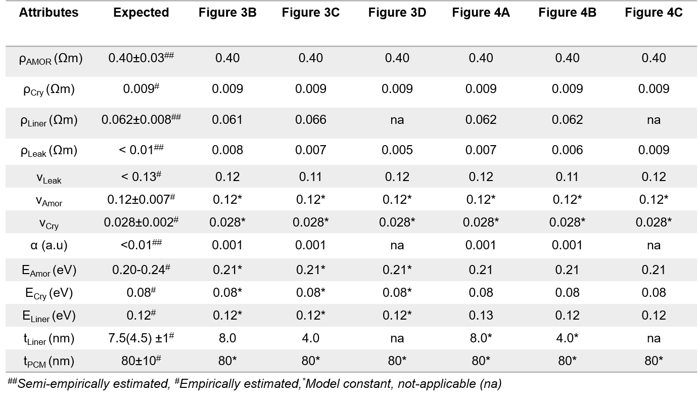
Having thus obtained the various important device metrics, we now investigate how the drift coefficients () in the unprojected and PMPCM devices scale as a function of . Figure 3A illustrates resistance vs time measurements of multiple resistance states in a mushroom-type device. By fitting such data with the standard resistance drift equation, we obtain the state-dependent drift coefficients. In Figure 3B, we plot the drift coefficients of the various unique resistance states in a 7.5 nm liner-based PMPCM device. An equivalent plot for an unprojected device is shown in section S3, from which we extract and of d-GST to be and , respectively. Thus, in a PMPCM device, we make two observations (see section S5). First that resistance drift is minimized: for RESET states, drift coefficients are reduced by a factor of 10. This is indicative of good projection efficacy. And second that the drift coefficients scale inversely with for small , plateau for an intermediate range of , and show a gradual rise for higher . In an ideal PMPCM device, the upper limit of drift coefficients is , since majority read current bypasses the amorphous dome (), and flow through the serial combination of and , where only has the tendency to drift. Therefore, the measured high drift coefficients for small indicates that a comparable current also traverses through the amorphous dome, along regions that structurally relax. This observation necessitates presence of a shunt resistor , which, from a circuit standpoint must be in parallel to . It is difficult to draw a physical picture of , although taking ideas from photovoltaics, may reflect the many randomly placed conductive pathways bridging the bottom electrode and in the device. In an alternate scheme, may be representative of extremely fine recrystallized amorphous like grains, at the amorphous-crystalline phase-change material interface (see section S6).
We fit the circuit model to this data, and in the spirit of capturing an accurate physical picture, we fit most parameters. The model can adequately trace the data (red trace in Figure 3B), and the various parameters output by the model’s fit are bracketed within the expected margins, which we estimated independently (see Table 1 ( and columns)). To gain further confidence on the scaling, we repeated the exact measurements, however on PMPCM devices with a 4.5 nm liner. One such measurement is shown in Figure 3C. We observe a similar trend in the drift coefficients with respect to but with some differences; namely the drift coefficients peak at higher values, the smallest drift coefficients are 2x higher than in thicker liner based PMPCM, and the region 3 is more pronounced. These characteristics indicate reduced projection efficacy in thinner liners based PMPCMs, and are simply a result of the higher sheet resistance of the liner, due to its small physical thinness. When is fitted to the circuit model, we find an adequate match, and the various parameters lie within the expected margins (see Table 1, column). To compare, in Figure 3D, we plot in an unprojected PCM device. Notably all resistance-states drift with , and when this experimental data is fitted to the model we observe adequate match (shown as a red trace), and the parameters have expected values (see Table 1, column). Such a device behavior can be simply explained by the fact that in an unprojected device, for , the read-current always (and only) traverses through the amorphous dome. Therefore, the drift coefficients can only take a value from a distribution around mean , independent of the . The measurement also hints at the nature of . It suggests that is bound to ; if it were greater, the unprojected devices should have shown higher drift coefficients. In Figure 3E, we plot the resistance vs of an unprojected device, and PMPCM devices with thinner (4.5 nm), and thicker (7.5 nm) liners. Much in the manner predicted by the circuit model, the unprojected device is more resistive for all . This follows equations 1 and 3, where the resistance scales as in an unprojected device, whereas in a PMPCM device dominantly by . Also observe that within PMPCM devices, the thinner liner devices are more resistive in the RESET states than thicker liner-based, due to the higher of the former.
We now discuss the mechanisms that lead to the dependency in PMPCM devices by sketching the different operational regimes (see Figure 3F, in which the thinnesses of the individual resistor wriggles encode resistance magnitude). In region 1, where the device is in the regime of a small , the effective amorphous dome resistance () is comparable to due to the small . Because these resistive elements are the only two pathways the read-out current (highlighted by green arrows) can take while traversing from the BE to TE, it equally splits. Since a large fraction of the current flows through the amorphous dome, which is the component drifting most in the circuit, the drift coefficients are high. In region 2, or for an intermediate , the effective amorphous dome resistance is large compared to due to large and . The implication is that a majority of read-current flows through the liner and not the amorphous dome, thereby yielding small drift coefficients. In region 3, where is large, the difference between the effective amorphous dome resistance and gets smaller through geometrical scaling of and , such that more and more read-current begins to flow through the amorphous dome. Through a different mechanism, this again leads to a reduction of the projection efficacy. Because this behavior is dictated by , thinner liners that have large are expected to show an early onset (at smaller ) of region 3, as has been experimentally noted.
Temperature dependent drift coefficients
Ambient temperature is yet another important state-variable that can impact device behavior. We now discuss the temperature dependence of the drift coefficients in unprojected and PMPCM devices. We perform these measurements by creating a RESET state and performing multiple resistance vs time measurements on it at different ambient temperatures (achieved through a heated sample stage). Figure 4A illustrates one such measurement in a 7.5 nm liner PMPCM device. We observe that the drift coefficients change proportionally with temperature. If a linear approximation is made, the drift coefficient sensitivity to temperature is a . We fit the data to the circuit model and note the model to adequately trace the data (see red trace), and all extracted parameters to be in expected range (see Table 1, column). We repeat the measurements on 4.5 nm liner-based PMPCM devices (see Figure 4B). Notably, the drift coefficients show similar temperature dependency, and when the data is fitted to the circuit model, it adequately matches (see red trace). The dependency indicates that the standard resistance drift equation is re-defined for PMPCM devices. This has important implications for in-memory computations since these devices are expected to operate under varying ambient conditions (in automotive, cloud for example). Note, however, that unlike for the dependency on , the drift coefficients in both the thinner and thicker liner PMPCM devices scale similarly. This indicates that the dependency arises from changes in the materials’ properties (and not geometry). To support these findings, we performed measurements on unprojected devices (see Figure 4C). Note that the device drifts with a constant drift coefficient at all temperatures (there is no dependency). When this data is fitted to the model we find an adequate match (see red trace) and the extracted parameters are bounded within margins (see Table 1, column).
The mechanisms that lead to the dependency in the PMPCM devices are discussed in Figure 4D. We present two cases, one where the device is at room temperature () and the other where it is at some elevated temperature (). At , the effective dome resistance is larger than , and therefore a majority of the read-current flows through the non-drifting and . As the ambient temperature increases, , , and decrease -not from changes in the , but from the thermally activated charge transport- since both the phase-change material and liner are semiconductors. What determines the dependency however is the extent to which the individual components change relative to each other. A measurement of the temperature sensitivity is the activation energy. In a PMPCM device since is greatest, drops most dramatically with temperature. Thus, at , although the resistance of both the amorphous dome and liner drop, the change in resistance of the amorphous dome is larger. This results in the read-current between the parallel pathways to get altered disproportionately, such that more current now traverses through the amorphous dome. Note that at large , , thus can be ignored.
Since the drift coefficient of the amorphous dome itself is temperature independent (from Figure 4C), and the effective dome resistance progressively approaches due to thermally activated charge transport, the device drifts with higher drift coefficients. We additionally verified this by simulating the dependencies for different using the circuit model (see section S7). It is observed that as the mismatch between and grows, the device becomes more temperature-sensitive. When equals , the drift coefficients show least temperature dependency. However, while such a materials science approach reduces the drift’s dependency, it amplifies the device’s resistance sensitivity to temperature. When approaches , the resistance state becomes more and more temperature-sensitive, which can prove detrimental to analog training/inference workloads or multi-level data storage. Thus, while materials can be optimized, adaptive software corrections could also be used (see section S7).
Conclusion
In this paper, we discussed the important material and electrical attributes of projected mushroom-type phase-change memories. Using a combined experimental and theoretical framework, we described how a conductive thin film (liner) when added to a mushroom device modifies the data read-out characteristics. In spite of similar programming and phase configurations to unprojected devices, we found the state-dependent resistance drift and temperature sensitivity to evolve differently in the projected devices. We observed the projection efficacy to be decisively determined by the liner’s physical thickness, and the mismatch of electrical resistivity and the electronic activation energy between the phase-change material and the liner. Our findings provide the first insights into how vertically configured projected memristive devices may fundamentally operate. The results lay a directed framework for building higher performing projected memory for computational-memory applications.
Acknowledgments
This work is supported by the IBM Research AI Hardware Center.
We also acknowledge support from the European Research Council through the European Union’s Horizon Research and Innovation Program under grant number . We would like to thank Geoffrey W. Burr and Vijay Narayanan for technical discussions and management support. We thank Linda Rudin for proofreading the manuscript.
Methods
Device fabrication and characterization: We fabricated Projected PCM devices based on a typical mushroom-type geometry by placing a projection liner between the heater and phase-change material. The devices comprise an 80 nm thick film of a doped- (d-GST) phase-change material, a sub-10 nm thick film of metal-nitride () liner, bottom and top electrodes, where the bottom electrode radius is 19 nm. The device is 540 nm wide, and equally broad. All material depositions were carried out using sputter depositions. The devices were made on an 8-inch wafer, and we observed spatial nonuniformity’s in the thicknesses of the different films. This was noted using ellipsometry measurements, and we took these variations into account in our analysis. We characterized the retention, threshold voltage, SET speed and resistance drift properties of the projected and unprojected devices. The results are discussed in the supporting information. We calibrated the FEM model using the activation energy measurements on unprojected devices. For simulations, the current flow in the device is modeled by enforcing the continuity equation at each mesh point, using the expression and , where is current density, is electrical conductivity, and is the voltage. The crystalline phase-change material conductivity follows a Poole-Frenkel-type activated-transport model. To capture the self-heating that governs the operation of these devices, the continuity equation is solved simultaneously with the energy conservation equation , where is the thermal conductivity of the material and is the local temperature in the device. The thermal properties of the materials here are assumed to follow both the Weidemann-Franz electronic relationship. All parameters including electrical and thermal interface (boundary) resistances are taken from measurements and tabulated in section S4. In our analytical modelling a device without the liner comprises only , and . When in both device types, the BE can be referred to as fully covered or blocked, in which case a fraction of current traversing from BE to TE must always flow through the resistive amorphous volume. In this case, the resistances of the BE and TE to current are insignificant and can be ignored. In our fitting to the temperature dependent drift coefficient, similar to resistivity anisotropy, we also considered anisotropy in . From fitting we observed , regardless data could also be fitted without anisotropy.
Device measurements: The electrical measurements were performed in a custom-built probe station. The temperature of the chuck was measured using a Lake Shore Si DT-670B-CU-HT diode. Devices were electrically contacted with high-frequency Cascade Microtech Dual-Z GSSG probes. DC measurements of the device state were performed with a Keithley 2600 System SourceMeter. AC signals were applied to the device with an Agilent 81150 A pulse function arbitrary generator. A Tektronix oscilloscope (DPO5104) recorded the voltage pulses applied to and transmitted by the device. Switching between the circuit for DC and AC measurements was achieved with mechanical relays. Note that in our measurements all READ operations were performed at 0.2 V. We extract , and by fitting the resistance vs temperature data to the Arrhenius equation of the form where, is resistance at temperature , is the device resistance at and other symbols have their usual meanings. We obtain the state-dependent by using the field equation. As a starting point, from a known and , we extract . For this we measure the current-voltage trace of a RESET state and fit the trace to the modified Poole-Frenkel transport model where, is the current (in A), is the voltage (in V), is the electrical charge, is the contact area (in ), is the trap density (in ), is attempt-to-escape from a trap (in ), is the inter-trap distance, is equivalent to , and other symbols have their usual meanings. For plot shown in Figure 2, using and approximating for 10 nm and , we extract as 37.40 nm, and = . From these, is obtained. The field equation is then used to determine for any other resistance state, by using the variable unique to that state and the constant . For the state-dependent drift measurements, the resistance vs time measurement was performed for duration. For temperature-dependent drift measurements, each data point was extracted from five resistance vs time measurements, each of duration, where after every such measurement the device was crystallized for extraction. By fitting resistance vs time data for each state with the resistance drift equation , we extracted the drift coefficients. Here, is the device resistance at time , and is the time elapsed after .
References
References
- (1) Zidan, M. A., Strachan, J. P. & Lu, W. D. The future of electronics based on memristive systems. Nature Electronics 1, 22 (2018).
- (2) Ielmini, D. & Wong, H.-S. P. In-memory computing with resistive switching devices. Nature Electronics 1, 333 (2018).
- (3) Mutlu, O., Ghose, S., Gómez-Luna, J. & Ausavarungnirun, R. Processing data where it makes sense: Enabling in-memory computation. Microprocessors and Microsystems 67, 28–41 (2019).
- (4) Sebastian, A., Le Gallo, M., Khaddam-Aljameh, R. & Eleftheriou, E. Memory devices and applications for in-memory computing. Nature nanotechnology 15, 529–544 (2020).
- (5) Sebastian, A. et al. Brain-inspired computing using phase-change memory devices. Journal of Applied Physics 124, 111101 (2018).
- (6) Kuzum, D., Jeyasingh, R. G., Lee, B. & Wong, H.-S. P. Nanoelectronic programmable synapses based on phase change materials for brain-inspired computing. Nano letters 12, 2179–2186 (2011).
- (7) Yu, S. Neuro-inspired computing with emerging nonvolatile memory. Proceedings of the IEEE 106, 260–285 (2018).
- (8) Wong, H.-S. P. et al. Phase change memory. Proceedings of the IEEE 98, 2201–2227 (2010).
- (9) Xiong, F., Liao, A. D., Estrada, D. & Pop, E. Low-power switching of phase-change materials with carbon nanotube electrodes. Science 332, 568–570 (2011).
- (10) Shukla, K. D., Saxena, N., Durai, S. & Manivannan, A. Redefining the speed limit of phase change memory revealed by time-resolved steep threshold-switching dynamics of aginsbte devices. Scientific reports 6, 1–7 (2016).
- (11) Sarwat, S. G. et al. Scaling limits of graphene nanoelectrodes. Nano letters 17, 3688–3693 (2017).
- (12) Le Gallo, M. & Sebastian, A. An overview of phase-change memory device physics. Journal of Physics D: Applied Physics 53, 213002 (2020).
- (13) Nardone, M., Kozub, V., Karpov, I. & Karpov, V. Possible mechanisms for 1/f noise in chalcogenide glasses: A theoretical description. Physical Review B 79, 165206 (2009).
- (14) Le Gallo, M., Tuma, T., Zipoli, F., Sebastian, A. & Eleftheriou, E. Inherent stochasticity in phase-change memory devices. In 2016 46th European Solid-State Device Research Conference (ESSDERC), 373–376 (IEEE, 2016).
- (15) Ielmini, D., Nardi, F. & Cagli, C. Resistance-dependent amplitude of random telegraph-signal noise in resistive switching memories. Applied Physics Letters 96, 053503 (2010).
- (16) Carboni, R. & Ielmini, D. Stochastic memory devices for security and computing. Advanced Electronic Materials 1900198 (2019).
- (17) Sebastian, A., Gallo, M. L. & Eleftheriou, E. Computational phase-change memory: beyond von neumann computing. Journal of Physics D: Applied Physics 52, 443002 (2019).
- (18) Sarwat, S. G. Materials science and engineering of phase change random access memory. Materials Science and Technology 33, 1890–1906 (2017).
- (19) Li, C. et al. Understanding phase-change materials with unexpectedly low resistance drift for phase-change memories. Journal of Materials Chemistry C 6, 3387–3394 (2018).
- (20) Ding, K. et al. Phase-change heterostructure enables ultralow noise and drift for memory operation. Science 366, 210–215 (2019).
- (21) Xiong, F. et al. Self-aligned nanotube–nanowire phase change memory. Nano letters 13, 464–469 (2013).
- (22) Shen, J. et al. Thermal barrier phase change memory. ACS applied materials & interfaces 11, 5336–5343 (2019).
- (23) Yang, W., Hur, N., Lim, D.-H., Jeong, H. & Suh, J. Heterogeneously structured phase-change materials and memory. Journal of Applied Physics 129, 050903 (2021).
- (24) Koelmans, W. W. et al. Projected phase-change memory devices. Nature communications 6, 8181 (2015).
- (25) Kersting, B., Ovuka, V., Jonnalagadda, V. & et al. State dependence and temporal evolution of resistance in projected phase change memory. Scientific Reports 10, 8248 (2020).
- (26) Kim, S. et al. A phase change memory cell with metallic surfactant layer as a resistance drift stabilizer. In International Electron Devices Meeting (IEDM), 30–7 (IEEE, 2013).
- (27) Kim, W. et al. Ald-based confined pcm with a metallic liner toward unlimited endurance. In International Electron Devices Meeting (IEDM), 4–2 (IEEE, 2016).
- (28) Redaelli, A., Pirovano, A. & Pellizzer, F. Phase change memory device for multibit storage, ep2034536b1 (2007).
- (29) Bruce, R., Ghazi Sarwat, S., Boybat, I. & et al. Mushrrom phase change memory with projection liner: An array-level demonstration of conductance drift and noise mitigation. IEEE, International Reliability Physics Symposium (Accepted) (2021).
- (30) Burr, G. W. et al. Phase change memory technology. Journal of Physics D: Applied Physics 52 (2019).
- (31) Wong, H. et al. Phase change memory. Proceedings of the IEEE 12 (2010).
- (32) Rajendran, B. et al. Dynamic resistance-a metric for variability characterization of phase-change memory. IEEE Electron Device Letters 30, 126–129 (2009).
- (33) R.Holm. Electric contacts theory and application (1967).
- (34) Sebastian, A., Papandreou, N., Pantazi, A., Pozidis, H. & Eleftheriou, E. Non-resistance-based cell-state metric for phase-change memory. Journal of Applied Physics 110, 084505 (2011).
- (35) Zheng, P. & Gall, D. The anisotropic size effect of the electrical resistivity of metal thin films: Tungsten. Journal of Applied Physics 122, 135301 (2017).
- (36) Salvadori, M. C., Cattani, M., Teixeira, F. S., Wiederkehr, R. S. & Brown, I. G. Anisotropic resistivity of thin films due to quantum electron scattering from anisotropic surface roughness. Journal of Vacuum Science & Technology A 25, 330–333 (2007).
- (37) PVEducation. Shunt resistance in solar cells, https://bit.ly/3nhj0ue. Accessed:2020–12-12.
- (38) Dhass, A. D., Natarajan, E. & Ponnusamy, L. Influence of shunt resistance on the performance of solar photovoltaic cell. In 2012 International Conference on Emerging Trends in Electrical Engineering and Energy Management (ICETEEEM), 382–386 (2012).
- (39) Mohammed, S. B. & Alamri, S. N. Modeling of photovoltaic module and experimental determination of serial resistance. Journal of Taibah University for Science 2, 94–105 (2009).
- (40) Athmanathan, A. Multi-level cell phase-change memory-modeling and reliability framework. Ph.D. thesis, Ph. D. Dissertation. EPFL (2016).
- (41) Neumann, C. M. et al. Engineering thermal and electrical interface properties of phase change memory with monolayer mos2. Applied Physics Letters 114, 082103 (2019).
- (42) Ma, C., He, J., Lu, J., Zhu, J. & Hu, Z. Modeling of the temperature profiles and thermoelectric effects in phase change memory cells. Applied Sciences 8, 1238 (2018).
- (43) Papandreou, N. et al. Estimation of amorphous fraction in multilevel phase-change memory cells. Solid-State Electronics 54, 991–996 (2010).
- (44) Ielmini, D. & Zhang, Y. Estimation of amorphous fraction in multilevel phase-change memory cells. Journal of Applied Physics 102, 054517 (2007).
- (45) Ielmini, D. Threshold switching mechanism by high-field energy gain in the hopping transport of chalcogenide glasses. Physical Review B 78, 035308 (2008).