Non-adiabatic quantum control of valley states in silicon
Abstract
Non-adiabatic quantum effects, often experimentally observed in semiconductors nano-devices such as single-electron pumps operating at high frequencies, can result in undesirable and uncontrollable behaviour. However, when combined with the valley degree of freedom inherent to silicon, these unfavourable effects may be leveraged for quantum information processing schemes. By using an explicit time evolution of the Schrodinger equation, we study numerically non-adiabatic transitions between the two lowest valley states of an electron in a quantum dot formed in a SiGe/Si heterostructure. The presence of a single atomic layer step at the top SiGe/Si interface opens an anti-crossing in the electronic spectrum as the centre of the quantum dot is varied. We show that an electric field applied perpendicularly to the interface allows tuning of the anti-crossing energy gap. As a result, by moving the electron through this anti-crossing, and by electrically varying the energy gap, it is possible to electrically control the probabilities of the two lowest valley states.
I Introduction
Adiabatic theorem and manifestations in single-electron pumps. According to the adiabatic theorem, a system initially in its ground state, and whose Hamiltonian evolves slowly in time, is expected to remain in the ground state of the instantaneous Hamiltonian, provided the ground state is non-degenerate. However, if the Hamiltonian varies quickly, then this approximation is no longer valid and the state is best described by a superposition of eigenstates of the instantaneous Hamiltonian. This superposition of states induces spatial oscillations of the wave-function, which are an observable manifestation of the violation of the adiabatic theorem. This is encountered in single electron pumps operating at fast pumping frequencies, where being in the non-adiabatic regime leads to a decrease in the accuracy and precision of the pump [1]. For instance, in the work of Yamahata et al. [2] non-adiabatic oscillations were experimentally measured in single-electron pumps formed by a silicon nanowire field effect transistor. They also presented a one-dimensional simulation of non-adiabatic oscillations between electron orbitals for a moving quantum dot and demonstrated the resulting spatial oscillations of the wave function.
Valleys in silicon and SiGe structures. In a [001] grown SixGe1-x heterostructure, the tensile strain between the Si and SiGe layers breaks the six-fold valley degeneracy of bulk silicon, leading to a four-fold degeneracy ( and valleys) raised in energy and a two-fold degeneracy ( valleys) lowered in energy. The latter can be further broken by interface roughness, impurities, or electric fields [3, 4]. It is sufficient to focus on the two lowest valley states because of the high energy gap (typically around 200 meV [3]) between them and the other and valley states.
Non-adiabatic transitions with valleys is unexplored. Whilst Yamahata et al. considered electron orbitals, they do not take into account the valley degrees of freedom inherent to silicon, which are expected to couple with the orbital states in any realistic device [5, 3, 6]. Hence it may be possible, due to valley-orbit coupling, to observe non-adiabatic transitions between valley states. Note that coherent oscillations between valley states has been previously studied in pure valley qubit schemes based on double quantum dots [7, 8], while we instead focus on a single quantum dot. Similarly, Boross et al. [9] considered coherent oscillations between valley states in a single dot, but their driving scheme is limited to a weak electric field, contrary to our scheme.
Model and contribution of the paper. In this paper, we study the dynamics of a single electron trapped in a quantum dot formed by a [001] grown Si0.8Ge0.2/Si heterostructure. The appearance of valley physics stems from our modelling of the SiGe/Si heterostructure by use of a two-band model. Non-adiabatic effects are then introduced by quickly varying the centre of the quantum dot potential. We then successively consider two two-dimensional models of a simplified SiGe/Si heterostructure, both introduced in section II.
In the first model, we present an ideally grown heterostructure, where the orbital degrees of freedom originating from the quantum dot are decoupled from the valley degrees of freedom, and thusly observe only non-adiabatic transitions between orbital states. An analytic study of such transitions is tackled in section III.
In the second model, we model a miscut SiGe/Si heterostructure by introducing a single atomic step at the interface, akin to that of Boross et al.. In section IV, we explain why the introduction of this step alters the spectrum of the system as the quantum dot position is varied. The key physics is that an anti-crossing between the two lowest valley states opens, with an energy gap tuneable by an electric field applied along the direction. This behaviour is verified by a realistic tight-binding calculation using NEMO 3D’s 20 band model [10]. We detail this in appendix A. As a result of the anti-crossing, the non-adiabatic pulsing of the electron through this step allows one to induce transitions from one valley state to another. Section V discusses the main result of the paper, namely that the final state can be electrically controlled by varying the anti-crossing energy gap. Due to the appearance of the avoided crossing in the spectrum, we model the transition using the Landau-Zenner approximation [11] and achieve good concordance. From studying the results there exists a range of driving parameters in which the final state forms a good two-level system, opening the door for qubit applications. We discuss the viability of such non-adiabatic valley qubit in section VI.
II Models
II.1 Ideal model
Quantum dot potential. We now present the two-dimensional model, in the plane, used throughout this paper. We assume the growth axis of our heterostructure to be orthogonal to the axis, as shown in figure 1. In the direction, the electron has a transverse effective mass . The quantum dot potential is a harmonic potential of angular frequency whose minimum follows a trajectory , hence . We choose such that we obtain an orbital level spacing 2 meV for the orbital states. This value is chosen to isolate the higher orbital states from the two lowest valley states. Note that the axis is neglected in our work since it does not affect the physics discussed.
Quantum dot trajectory. The evolution in time of the quantum dot position is the only source of time-dependence in Hamiltonian. The quantum dot is initially at position nm at ps, and moves with constant velocity until it reaches at time . The parameters and are varied to obtain different values for . The trajectory of the quantum dot can be written:
| (1) |
The Hamiltonian describing the dynamics along the axis is
| (2) |
and is identical for all in the ideal model.
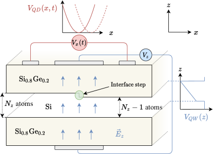
Description of the confinement. The confinement and the valley effects are modelled using the tight-binding model for strained silicon quantum wells of Boykin et al. [13, 12]. The resulting Hamiltonian for the slices depends on three parameters: the onsite energy , the nearest neighbor hopping and the second-neighbor hopping giving the Hamiltonian in equation 3.
| (3) |
In this Hamiltonian, each site represents an atom of the quantum well in the axis. We will define to be the total number of atoms in the axis, where each atom is separated by Å. We will also refer to as the quantum well width, expressed in number of atoms. A monolayer corresponds to two atoms, so that our choice of quantum well width corresponds to 20 monolayers. Note that varying the width of the Si/SiGe quantum well, as we could do in the simulations, is experimentally feasible.
Expected eigenstates and spectrum. In our model, the quantum well width is nm. The energies of this infinite quantum well barrier are given by with the electron’s longitudinal effective mass and the orbital number. The energy gap between the first and second quantum well eigenstates is then meV. Because of this high energy gap, it is reasonable to only consider the first eigenstate of the quantum well. The eigenstates of , which are eigenstates of the harmonic oscillator, are denoted by with describing the orbital number.
The Hamiltonian describing the confinement gives a valley splitting less than the orbital spacing induced by to the harmonic oscillator. As a consequence, we expect to observe two well defined valley states for each orbital. We will denote the corresponding eigenstates and energies , with where is the orbital index and the valley index. It will be convenient later on to index the states and the energies with a single index for readability. Since the valley states always have lower energies than the states for a given , we will use the natural mapping , , and so on to label the energies and eigenstates by increasing energies. The meaning of the indices will be understood from context depending on whether there is one or two indices.
As a final note, the full Hamiltonian for this idealised model is separable in and , and hence the valley degrees of freedom do not couple to the orbital degree of freedom. The eigenstates are the product of the eigenstates of the Hamiltonians and , and indeed the indices are good quantum numbers.
II.2 Single step model
Description of the interface step, and experimental justification. As in the work of Boross et al., we introduce an interface step consisting of a single atomic layer at nm, modelled by decreasing the width of the quantum well for all slices where (see figure 1). This interface step is motivated by the single atomic layer steps observed in SiGe/Si heterostructures grown on slightly vicinal [0 0 1] Si substrates [14, 15, 16, 17]. In particular, these steps occur at polar miscut angles , with terrace width on the order of 10nm [15, 16, 17]. Given can be controlled by manufacturers to within [14] and uniform terrace width can be achieved as in [15], one could manufacture a structure with an interface step similar to that modelled in this paper.
Differences with Boross et al.. Unlike Boross et al., we do not allow the wave function to penetrate inside the SiGe layer, instead enforcing hard-wall boundary conditions, however, the physics observed is expected to be similar. And indeed as shown in figure 5, the evolution of the spectrum is similar to that obtained in Boross et al.. Another difference in our work is that we do not limit ourselves to weak perturbations along the axis: we study the opposite limit of strong non-adiabatic perturbations. Furthermore, our modelling has been validated with NEMO 3D’s 20 band model, see appendix A.
II.3 Methods
We numerically solve the ground state of the total Hamiltonian at the initial time ps and use this result as the initial wave function for solving the time-dependent Schrödinger equation. The time-dependent Schrödinger equation is solved using the Crank-Nicolson scheme [18]. The onsite energy parameter of (equation 3) is set to 1.395 eV such that the spectrum has negative values close to zero, allowing for easier differentiation between “real” eigenvectors and “artificial” eigenvectors (eigenvalues of 0). Indeed, this is necessitated by the setting the column and row of the relevant lattice sites to zero in the Hamiltonian to produce the step in the interface, described above, as this introduces null eigenvalues. The difference between our chosen value of and the choice made in Boykin et al. is then restored after diagonalisation. The values used for the off-diagonal elements can be found in figure 2 of Boykin et al. [12].
In all simulations, we fix nm and ps. For the simulations involving the ideal model, we fix to 5 ps and vary to change . This choice ensures that the perturbation is applied for the same amount of time in all simulations. For the step model however, we fix nm and vary to change . As discussed later, the spatial evolution of the dot relative to the step is critical for analysis of the simulations, such that fixing the initial and final positions and changing the time is the more appropriate choice of altering the velocity.
III Non adiabatic effects in the ideal model
III.1 Preliminary remarks
Introduction. In this section, we comment on the numerical results obtained with the ideal model (figure 2) of section II.1, i.e when no interface step is present. As explained in the previous section, the Hamiltonian is separable in the and coordinates. Since the time-dependence only originates from the axis, the dynamics of the system reduce to that of a driven quantum harmonic oscillator described by the Hamiltonian of equation 2. As a consequence, the only parameter we vary in our simulations is the quantum dot speed (in particular, the applied electric field does not influence the numerical results). This model is essentially the same as the one from Yamahata et al. [2], with the difference being the trajectory of the quantum dot. Our choice for the trajectory (see equation 1) will simplify the interpretation of the numerical results.
Oscillatory features of the probabilities: amplitude and period. As a preliminary remark, one can notice that the states of energy have a zero probability of occupation for all time. Indeed, since the dynamics only originate from the orbital degree of freedom, and no valley orbit coupling exist in this ideal model, no transition to a state of valley index can happen because we started in a state with .
A second striking feature is the oscillatory behaviour of the probabilities. Noticeably, the period of the oscillations is constant (it depends only on the potential of the quantum dot), but the amplitude can be increased through . An analytical derivation of this fact is performed in the next subsection under the adiabatic approximation. Note, however, that higher values of slowly increase the probabilities of higher orbital states (i.e states with ), as can be seen in the last row. For low values of , the coherent oscillations between the two states are effectively Rabi oscillations encountered in qubits, but this does not hold at higher quantum dot speeds.
Classical analogy and spatial oscillations of the probability density. A consequence of the presence of states other than the ground state manifests itself in the spatial oscillations of the probability density. The spatial oscillations of the electron can easily be understood classically as follows. Applying the Heisenberg equation of motion to the operators and , we obtain:
From which we can derive the following equation of motion for :
| (4) |
This is exactly the equation of motion of a classical harmonic oscillator driven by some force . Hence we see that the average position behaves exactly as in the classical case of a driven harmonic oscillator. The period of the spatial oscillations depends only on and not on the initial conditions, whilst the amplitude increases with an increase in the driving force.
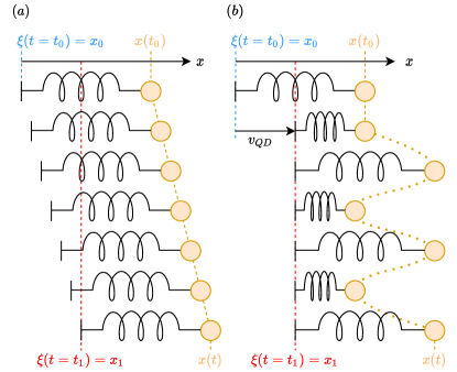
Classically, the movement of the quantum dot can be understood by pushing a spring to which a mass is attached, as shown in figure 3. Pushing the spring adiabatically, the mass is expected to follow the movement of the spring, i.e adapt to the perturbation at each time. However, pushing the spring over the same distance during a shorter period of time, one expects the mass to oscillate, as it does not have time to adjust to the perturbation.
Spatial oscillations from a quantum superposition. Returning to the quantum case, one can assume that the effect of a non-adiabatic perturbation is to put the wave function into a superposition of states. For instance, assuming that at the end of the quantum dot’s trajectory, i.e for , and for relatively low values of , the state is of the form:
where and are respectively the ground and first excited state of the harmonic oscillator at , and if the state probability. Since for the Hamiltonian becomes time-independent (it corresponds to a harmonic oscillator centred at ), the time evolution of the state is of the form:
with and period corresponding to a pulsation . Note that here the superposition is time-dependent but the state probability is time-independent, since the probability does not depend on time.
The average position for can then be expressed as:
where we have used equation (4.174) of reference [19] to write . Hence, we recover the fact that the probability density oscillates in space, due to a quantum superposition of states. These spatial oscillations of the probability density are at the root of the oscillations experimentally observed by Yamahata et al..
III.2 Transition probabilities in the weak non-adiabatic regime.
In this section, we follow a method by B. H. Bransden [19] to derive an analytical expression for the probability of the first orbital excited state, i.e the state . To simplify notations, we will drop the time-dependence of and denote by the electron’s transverse effective mass and the Hamiltonian. We will also make use of the single index notation defined in section II, such that we study the transition . One can expand the Hamiltonian of the 1D model as follows:
The derivative with respect to time comes out as:
| (5) |
Following B. H. Bransden, the probability amplitude of the first orbital excited state under the adiabatic approximation is (equation 9.100):
| (6) |
with denoting the eigenstates of the harmonic oscillator centred at . We can simplify the numerator using equation 5:
Using the generating function for the Hermite polynomials (see equation (4.174) of reference [19]), one has the following identity:
| (7) |
Hence:
We can then obtain a more explicit expression for the probability amplitude of the first orbital excited state:
At this stage, it is useful to introduce the maximum speed of a quantum harmonic oscillator in the ground state. Assuming that the total energy corresponds to kinetic energy, we have , where the maximal speed. We can then rewrite the expression for as:
| (8) |
For , we can obtain the transition probability from the modulus squared of :
| (9) |
Hence, the state probabilities oscillate with an amplitude proportional to as observed in figure 2. The period of oscillations can be made more apparent by rearranging the equation above:
with as previously defined. In the context of our simulations, the orbital spacing meV gives ps, which matches the period observed in figure 2.
In appendix B, a similar calculation is performed to estimate the probability of the second excited orbital state .
III.3 Criterion for the transition to the non-adiabatic regime
Strictly speaking, an adiabatic evolution implies that the probability of being in eigenstate remains the same throughout the infinitely slow perturbation. For instance, if the initial probability of the state is initially zero, then it should continue being zero at all future times. In practice, it is convenient to adopt a less restrictive definition by comparing how well an adiabatic approximation matches with the actual results.
Using equation 9 we can find an upper bound for the probability of the first orbital in the adiabatic approximation, namely the maximum value of is given by
| (10) |
As the bound is directly proprtional to the square of (the orbital spacing is fixed to 2 meV), one can appreciate that the physics is particularly sensitive to the quantum dot speed. This upper bound is plotted in figure 4 (blue solid line).
As discussed in the previous subsection, and considering the results of figure 2, the value of the final probabilities depend on the time at which we look for a fixed value of . As a consequence, we plot in figure 4 the the maximum value of the probability of depending on , as obtained from the simulations (red dashed line).
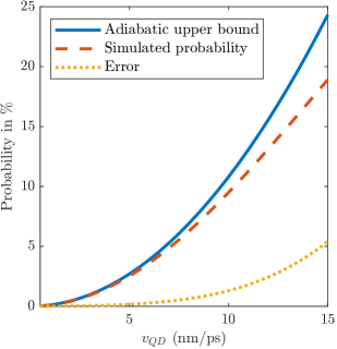
We remark that the numerical data matches the adiabatic approximation for low , i.e when the adiabatic approximation is valid. However, as increases, the adiabatic approximation, utilised to derive the analytic expression, becomes invalid and the difference between the upper bound and the numerical results widens as expected. Indeed, this can easily be interpreted by looking at the results of figure 2 where we see higher orbital states appearing as increases. As a consequence, some of the probability leaks to these higher orbital states, explaining why the results diverge. The yellow dotted line gives an estimation of how “non-adiabatic” the system is. Low values testify to an adiabatic system for the orbitals, while values above a certain threshold (arbitraly chosen) indicate a non-adiabatic regime.
To conclude this section, we would like to emphasise that the plot of figure 4 only considers the orbital degrees of freedom, as the valley degrees of freedom do not play a role in the ideal model. Still, figure 4 will prove useful for analysing the results involving the valley degrees of freedom of the step model, discussed in section V.
IV Spectrum in the step model
We now perform the same analysis but with the step model. Critically, the perturbation now couples the orbitals with the valley states of the electron.
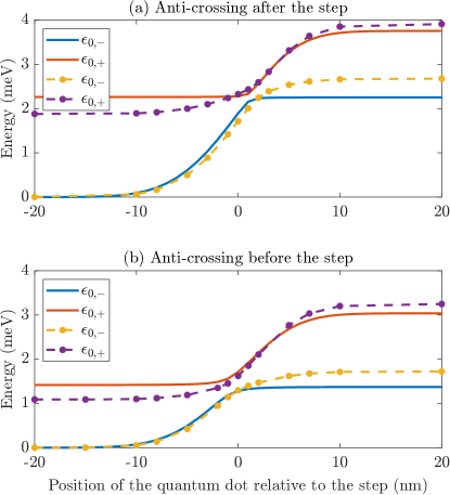
General remarks on the spectrum. We now discuss the salient features of the spectrum of the step model as the minimum of the quantum dot potential is varied. The results are plotted in figure 5 for different electric fields . To simplify notations, we continue to label the energies with the indices , but one should be reminded that near the step, the strong valley-orbit coupling prevents from being good quantum numbers. Note that far away from the steps, the wave functions are well defined valley states, and the indices are still good quantum numbers.
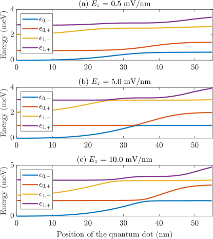
Origin of the anti-crossing. A critical observation is the existence of an anti-crossing near the step location (at nm). As mentioned in the previous paragraph, the step causes the coupling of the valley and orbital degrees of freedom. In the absence of disorder at the well interface there exists globally defined valley states, where the valley states are translationally invariant, however, the step potential explicitly breaks this symmetry resulting in the observed anti-crossing.
The physics behind this avoided crossing can be understood by examining the probability density of the two lowest energetic states, and is well described in Boross et al.. Indeed, as shown in both atomistic simulations [13, 12] and effective mass theories [20, 5], the wave functions exhibit modulations on the atomic scale of the envelope function. The two lowest valley states are symmetric and anti-symmetric superpositions of with , where Å is the lattice spacing of the silicon crystal. The atomic scale oscillations of the two valley states are similar except for a spatial de-phasing. A consequence of this spatial de-phasing is that one of the state will have a maxima at the step location, while the other will have a minima. Hence, as the quantum dot goes through the step, the lowest energetic state will feel the step, increasing its energy, while the other will not.
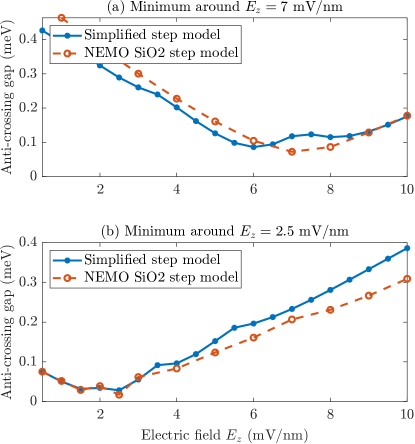
Control of the anti-crossing gap with electric field. As shown in figure 5, the energy gap at the anti-crossing of the two lowest valley states can be electrically controlled through the applied electric field . The dependence of the gap with the electric field is non-trivial and also depends on the quantum well width, which we have fixed to atoms in this paper. As discussed in later sections, the values of for which the energy gap of the anti-crossing is small will prove particularly useful for electrical control of the final state. One could question whether this behaviour is expected in real devices, or if it is an artifact of the two-band model we are using to model the valleys. In appendix A, NEMO 3D calculations using a 20 band model show that the gap at the anti-crossing is indeed controllable with the electric field . Akin to the results of the two-band model, the anti-crossing gap varies in the same non-trivial way, but it seems the trend can be reproduced only for certain quantum well widths. As a result, we expect the control of the anti-crossing gap to be feasible in real devices.
Higher orbital anti-crossing. We notice that a similar anti-crossing happens between valley states of higher orbitals too (states of energies and ). However, this anti-crossing happens before that of the ground state orbital. This makes sense since the higher orbital states of the harmonic oscillators have a wider spatial extent over the position as the orbital number increases. In turn, the step is felt earlier, explaining the earlier appearance of the anti-crossing.
V Non-adiabatic effects in the step model
V.1 General comments
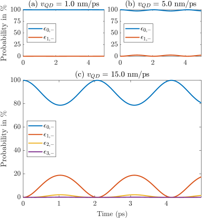
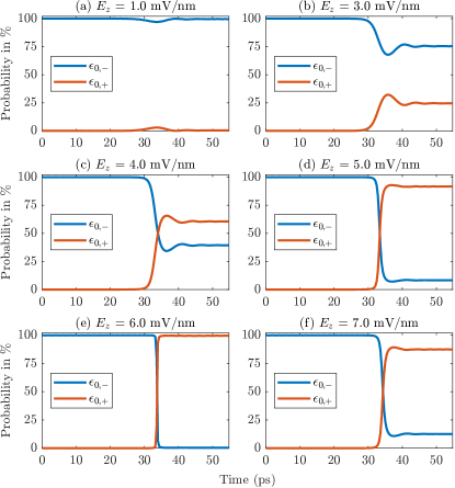
Results at a fixed low quantum dot speed. The movement of the quantum dot potential has the effect of bringing energy into the system. This additional energy allows the ground state to overcome the anti-crossing gap observed in the spectrum. As intuitively expected, the smaller the gap between the two lowest eigenstates, for the same perturbation the stronger the probability of transitioning to other valley states. This is illustrated well in figure 6 for nm/ps where the value of is small enough that the system is mostly confined to the two valleys of the first orbital state (this can be verified by examining the yellow dashed line of figure 4, showing that the perturbation is adiabatic for the orbitals). For this fixed quantum dot speed, the variation of the applied electric field is the only parameter used to tune the final probabilities of the valley states. Comparing the gaps in the spectra of figure 5 and the final probabilities of figure 6, one can relate the final probabilities to the tuning of the anti-crossing gap.
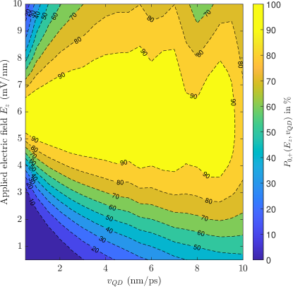
Results for different combinations of quantum dot speeds and electric fields. In the ideal model, the final probabilities were tuned through (see figure 4). In the step model too, the quantum dot speed can be used to tune the final probabilities. In figure 7, we plot the probability of the state for a combination of electric fields and quantum dot speeds . As expected from the spectra of figure 5, the “sweet spot” for transitioning to the state corresponds to small anti-crossing gaps, which happens in a range of electric fields mV/nm. One can also remark that increasing the quantum dot speed increases the transition probability for relatively small values of . For higher values of however, the transition probability actually decreases with increasing , since transition to higher orbital states starts to take place instead. This is easily interpreted from figure 4, which testifies to the presence of higher orbital states.
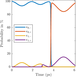
Higher orbital valley flipping. The spectra of figure 5 show that an anti-crossing exists between the states of the first excited orbital. Since the transition between valley states is due to the anti-crossing, it is legitimate to expect valley flipping behaviour for the first excited orbital. Still, according to the spectrum, this valley exchange should happen before that of the ground orbital states, as the anti-crossing happens at an earlier position as explained in section IV. This behaviour is indeed verified at higher quantum dot speeds as shown in figure 8.
V.2 Landau-Zener approximation
Standard Landau-Zener formula and anti-crossings. The probability of non-adiabatic transitions in a two-level system with an avoided crossing has been heavily studied, see reference [11] for instance. In particular, the Landau-Zener formula can be used to estimate the transition probabilities due to non-adiabatic effects. The benefit of such an analysis is that one can simply compute the final state probabilities without solving the full time-dependent Schrödinger equation.
Under the Landau-Zener approximation, the energy separation between the uncoupled states is a linear function of time with gradient , which is assumed to extend over all time. Furthermore, we denote the coupling induced by the step potential as and also assume it is constant in time. Knowing this, we can define
| (11) |
where the probability of transitioning to the excited state is given by the formula
| (12) |
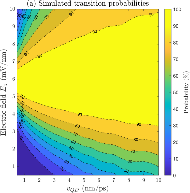
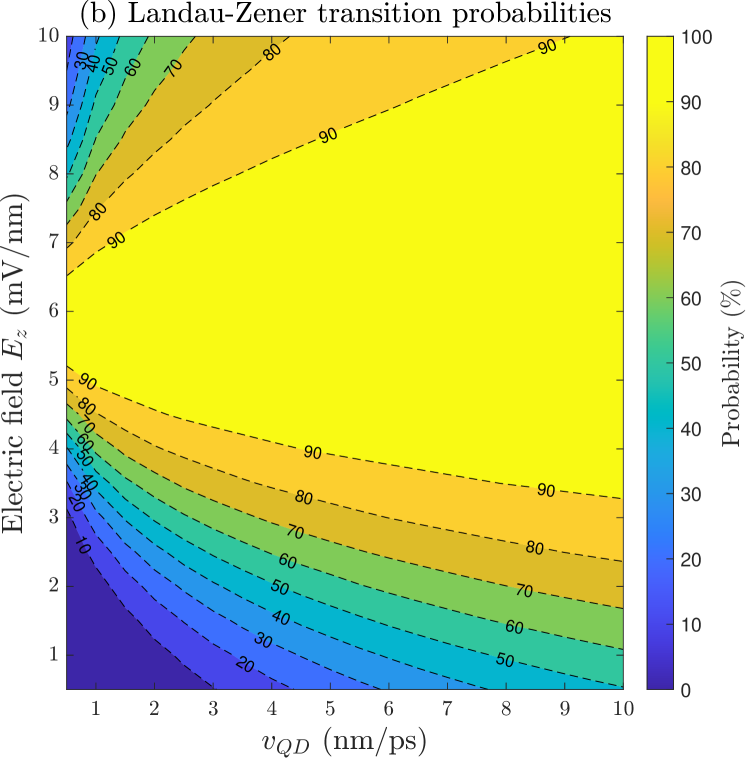
Fit to Landau-Zener. In a realistic model the perturbation is only linear over a finite range of time, as our numerical results for the spectra show in figure 5. An analytical modelling of our spectra is complicated, as the expression of the wave functions is not analytical in a quantum well with an applied electric field. As a consequence, we take the approach of fitting our numerical results to a simpler model. Luckily, such a simpler model is provided by Rubbmark et al. [11]. Hence we fit the energy level separation between the two lowest energy states () to equation (18) of reference [11] reproduced below ( and are the fitting parameters). The resulting transition probabilities are plotted in figure 9.b for different values of and .
| (13) |
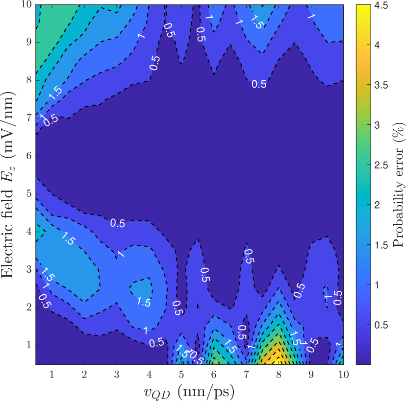
A surprising result is that the evolution of the transition probabilities is well captured by the Landau-Zener fit for almost all electric field values and the quantum dot speeds. In figure 9.a, the simulated transition probabilities are plotted. The Landau-Zener approximation in figure 9.b shows the same evolution as that of our numerical results. In figure 10, we plot the difference between the simulated transition probabilities and the ones obtained from the Landau-Zener approximation . This illustrates that the Landau-Zener approximation deviates only slightly from our numerical results. However, one should note that for large one would certainly observe transitions to higher orbitals and valley states whilst Landau-Zener only considers the transition to the other state in the two-level system. Regardless, the maximum value of the relative error across all values of electric field and quantum dot speed was only 1.0% (not shown in figure 10), and hence it provides a good measure of weather the electron is in the ground state or not - with perhaps no qualification on which state is has transitioned to.
VI Qubit application
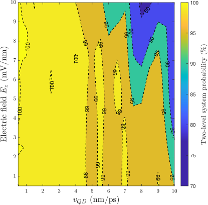
Validity of the two-level system and qubit application. The choice of the wide energy level spacing meV for the orbital states allows one to prevent transitions to higher orbital states, thus allowing for a two level valley system to form. However large values of can still lead to leakage to higher orbitals, and the electric field also plays a complex role. Regardless, there does exist a range of parameters for which the probability of higher orbital states is negligible and a set of qubit basis states is realised. We can estimate the range of parameters for which the final state is a two-level system numerically by summing the probabilities of the two states and forming our preferred two-level system. Using the two lowest energy states as a computational basis, our model effectively describes the time-evolution of a pure valley qubit with all-electrical control.
Coherence time and protection from charge noise. The use of the valley degrees of freedom to encode the quantum information is interesting in that it provides certain immunity to charge noise [21]. Charge noise is one of the leading sources of decoherence of silicon qubits [22, 21, 23, 24]. The resistance to charge noise has been experimentally verified through Laudau-Zener interferometry in a Si/SiGe double quantum dot by Mi et al. [25]. Previous implementations of qubits leveraging valley states in double quantum dots have shown a coherence time on the scale of nanoseconds [26, 27, 7, 8]. Although those qubits were implemented in double quantum dots, whilst our system is a single quantum dot, we expect the coherence time of our architecture to have a similar order of magnitude.
Experimental advantage. The all-electrical control of the final state probabilities is critical for scalability, as one would not need magnetic fields for qubit manipulation as in most spin qubit implementations [23, 24]. The absence of applied magnetic field, and hence microwave lines, makes the integration of such a system significantly more simple. A second advantage is that we are not constrained by any adiabatic condition, as a consequence, provided the decoherence times are similar to that of other hybrid valley qubits, we can perform orders of magnitude more gate operations.
Coupling, readout and other issues. Serious difficulties are to be overcome for this scheme to be usable in practice. First, engineering the electrical pulses used in our simulation may be challenging to implement. Indeed, the engineering required to control the spatial evolution of the quantum dot potential, i.e the trajectory , may be complicated due to the time scales involved. As argued by Boross et al., it may be somewhat achievable using a double quantum dot architecture and varying the barrier and detuning to move the electron through the step [28, 2]. This will inevitably be complicated by the additional gates needed to apply the electric field , due to the existence of cross couplings. On the other hand, we have been limiting ourselves to constant speeds for , and hence more complicated trajectories are unexplored and may be fruitful.
Finally, both readout and coupling to other such qubits has not been explored and may pose a significant technical challenge for the scalability of the proposed scheme. A potential avenue towards readout could be implemented with a form of charge sensing, as is done in most silicon qubits [24]. This would require the incorporation of another dot after the step, and adjusting the energy levels so that only the highest energy valley states tunnels to the second dot.
VII Conclusion
To summarise our work, we have shown that displacing a quantum dot potential through an interface step leads to an anti-crossing in the spectrum of the two lowest energetic states. A critical observation, which was verified with tight-binding calculations of NEMO 3D, is that the energy gap at the anti-crossing can be controlled by applying an electric field perpendicular to the interface. Since the transition probabilities depend on the energy gap, and the latter is electrically controlled, we can achieve all-electrical control of the final state probabilities. There is a range of parameters for which the final state behaves as a charge qubit encoded on valley states, though readout and coupling have not been explored.
There are two main limitations of our results. The first is the qualitative nature due to our highly idealized modelling. Indeed, we enforced hardwall boundary conditions for the confinement, so that the wavefunction does not penetrate through the SiGe layers, while a more realistic choice would be adding a finite height barrier of around 150 meV. We also neglected both the strain and alloy disorder of the Ge atoms. We also note that our work is only valid in the low density limit hence ignoring both Coulomb and exchange effects. Despite these remarks, the results obtained from NEMO 3D indicate that the physics discussed should still be applicable to real devices, with only qualitative modifications. Finally, the precise engineering of both the device geometry and the applied voltages for adequate control poses additional experimental challenges.
The second limitation is due to the experimental feasibility, namely the precise control of the fast electrical pulses to move the quantum dot and the existence of a single atomic step. Indeed, we expect multiple steps to form over the spatial range chosen for our simulations. We have also neglected relaxation mechanism, as these are supposed to occur on a timescale greater than the operation times.
Nevertheless, non-adiabatic control of valley states may open novel quantum information processing schemes. In this work, we have limited ourselves to the study of a single quantum dot, but we suspect that the results could be adaptable to more complicated double dot systems making the possible implementation of these ideas more realistic. Additionally, in some emerging 2D and topological materials, spin and valleys are strongly momentum locked, thus fast manipulation of valleys could lead to non-adiabatic control of spins.
Acknowledgements.
We acknowledge useful discussions with Edyta Osika concerning alternative simulation methods, and Vyacheslavs Kashcheyevs concerning the anti-crossing. This work is was partly funded under the Nicolas Baudin initiative and Thales Australia. Associate Professor Rajib Rahman acknowledges support from the US Army Research Office under grant number W911NF-17-1-0202. The research was undertaken with the assistance of re-sources and services from the National Computational Infrastructure (NCI) under NCMAS 2020 and 2021 allo-cation, supported by the Australian Government. This work was also supported with supercomputing resources provided by the Phoenix HPC service at the University of Adelaide.Appendix A Validation of the model
Objective. The Boykin et al. two-band tight-binding model has been verified in a Si/SiGe quantum well with flat hardwall boundary conditions [12] but it has not yet been used to model a quantum well with a monatomic step interface. Most results discussed in the main text depend on two critical facts: the existence of an anti-crossing between the two lowest valley states, and the relative control of the anti-crossing gap with the electric field . In this appendix, we compare the results obtained from the step model with those obtained with NEMO 3D’s 20 band model [10].
NEMO model. In our step model of subsection II.2, we used hardwall boundary conditions, which corresponds to an infinite barrier height. To model this in NEMO 3D, we utilised a SiO2 interface which has a large barrier height of eV. To reduce simulation time, we also adopted a tighter confinement for the quantum dot. The curvature of the quantum dot was set to meV/nm2 in all results presented in this appendix.
Limitations. In their paper, Boykin et al. showed that the two-band model they proposed correctly reproduced the trends expected for the valley splitting evolution with the width of the quantum well. In particular, the valley splittings have the correct order of magnitude but differ from NEMO 3D calculations. As such, their model is qualitative and not quantitative, and we expect to observe the same differences with our model. Similarly, we shall focus on only verifying that the critical trends necessary for our conclusions, namely the anti-crossing and the control of the energy gap, are mirrored by NEMO 3D.
Results. In figure 12, we compare spectra obtained using our step model (solid lines) and those obtained from NEMO 3D calculations (dotted lines). The reference energy was set to 0 to facilitate the comparison of both spectra. We remark that in both simulations, the location of the anti-crossing can happen before or after the step depending on the quantum well width. In both cases, the existence of the anti-crossing is verified by NEMO 3D.
Similarly, the tuning of the anti-crossing gap with the electric field is observed in both simulations, as shown in figure 13. As mentioned in the main text, the tuning of the gap with the electric field depends on the quantum well width. Some key features are exhibited by both our step model and the NEMO 3D calculations. Namely, the range of the tuning of the gap, the existence of a minimum, and the location of this minimum all depend on the quantum well width.
Appendix B Estimation of the probability of the second excited orbital state in the ideal model
In this appendix we estimate the form of the probability of the state in the ideal model. We adopt the notations of section III.2. From equation (4.174) and (9.97) of reference [19], we can estimate that the probability amplitude of the second excited state is related to the amplitude of the first excited state by:
Following equation 7, we find that . Using equation 8 we find:
The integration is straightforward and gives:
Finally, the transition probability to the second excited state can be computed as:
| (14) | ||||
Comparing equation 9 and equation 14 we see that the probability of the electron being in the state at time is the square of it being in the state .
References
- Kaestner and Kashcheyevs [2015] B. Kaestner and V. Kashcheyevs, Non-adiabatic quantized charge pumping with tunable-barrier quantum dots: a review of current progress, Reports on Progress in Physics 78, 103901 (2015).
- Yamahata et al. [2019] G. Yamahata, S. Ryu, N. Johnson, H.-S. Sim, A. Fujiwara, and M. Kataoka, Picosecond coherent electron motion in a silicon single-electron source, Nature Nanotechnology 14, 1019 (2019).
- Zwanenburg et al. [2013] F. A. Zwanenburg, A. S. Dzurak, A. Morello, M. Y. Simmons, L. C. L. Hollenberg, G. Klimeck, S. Rogge, S. N. Coppersmith, and M. A. Eriksson, Silicon quantum electronics, Reviews of Modern Physics 85, 961 (2013).
- Rahman et al. [2011] R. Rahman, J. Verduijn, N. Kharche, G. P. Lansbergen, G. Klimeck, L. C. L. Hollenberg, and S. Rogge, Engineered valley-orbit splittings in quantum-confined nanostructures in silicon, Phys. Rev. B 83, 195323 (2011).
- Friesen and Coppersmith [2010] M. Friesen and S. N. Coppersmith, Theory of valley-orbit coupling in a si/sige quantum dot, Phys. Rev. B 81, 115324 (2010).
- Tariq and Hu [2019] B. Tariq and X. Hu, Effects of interface steps on the valley-orbit coupling in a si/sige quantum dot, Phys. Rev. B 100, 125309 (2019).
- Schoenfield et al. [2017] J. Schoenfield, B. Freeman, and H. Jiang, Coherent manipulation of valley states at multiple charge configurations of a silicon quantum dot device, Nat Commun 8, 10.1038/s41467-017-00073-x (2017).
- Penthorn et al. [2019] N. Penthorn, J. Schoenfield, and J. e. a. Rooney, Two-axis quantum control of a fast valley qubit in silicon, npj Quantum Information 5, 10.1038/s41534-019-0212-5 (2019).
- Boross et al. [2016] P. Boross, G. Széchenyi, D. Culcer, and A. Pályi, Control of valley dynamics in silicon quantum dots in the presence of an interface step, Phys. Rev. B 94, 035438 (2016).
- Oyafuso et al. [2002] F. Oyafuso, G. Klimeck, R. Bowen, and T. Boykin, Nanoelectronic 3-d (nemo 3-d) simulation of multimillion atom quantum dot systems, in International Conference on Simulation of Semiconductor Processes and Devices (2002) pp. 163–166.
- Rubbmark et al. [1981] J. R. Rubbmark, M. M. Kash, M. G. Littman, and D. Kleppner, Dynamical effects at avoided level crossings: A study of the landau-zener effect using rydberg atoms, Phys. Rev. A 23, 3107 (1981).
- Boykin et al. [2004a] T. B. Boykin, G. Klimeck, M. Friesen, S. N. Coppersmith, P. von Allmen, F. Oyafuso, and S. Lee, Valley splitting in low-density quantum-confined heterostructures studied using tight-binding models, Phys. Rev. B 70, 165325 (2004a).
- Boykin et al. [2004b] T. B. Boykin, G. Klimeck, M. A. Eriksson, M. Friesen, S. N. Coppersmith, P. von Allmen, F. Oyafuso, and S. Lee, Valley splitting in strained silicon quantum wells, Applied Physics Letters 84, 115–117 (2004b).
- Teichert [2002] C. Teichert, Self-organization of nanostructures in semiconductor heteroepitaxy, Physics Reports 365, 335 (2002).
- Mysliveček et al. [2002] J. Mysliveček, C. Schelling, F. Schäffler, G. Springholz, P. Šmilauer, J. Krug, and B. Voigtländer, On the microscopic origin of the kinetic step bunching instability on vicinal si(001), Surface Science 520, 193 (2002).
- Evans et al. [2012] P. G. Evans, D. E. Savage, J. R. Prance, C. B. Simmons, M. G. Lagally, S. N. Coppersmith, M. A. Eriksson, and T. U. Schülli, Nanoscale distortions of si quantum wells in si/sige quantum-electronic heterostructures, Advanced Materials 24, 5217 (2012).
- Phang et al. [1994] Y. H. Phang, C. Teichert, M. G. Lagally, L. J. Peticolos, J. C. Bean, and E. Kasper, Correlated-interfacial-roughness anisotropy in /Si superlattices, Phys. Rev. B 50, 14435 (1994).
- Crank and Nicolson [1947] J. Crank and P. Nicolson, A practical method for numerical evaluation of solutions of partial differential equations of the heat-conduction type, Mathematical Proceedings of the Cambridge Philosophical Society 43, 50–67 (1947).
- B. H. Bransden [2000] C. J. J. B. H. Bransden, Quantum Mechanics, 2nd Edition (Pearson, 2000).
- Friesen et al. [2007] M. Friesen, S. Chutia, C. Tahan, and S. N. Coppersmith, Valley splitting theory of sige/si/sige quantum wells, Phys. Rev. B 75, 115318 (2007).
- Culcer et al. [2012] D. Culcer, A. L. Saraiva, B. Koiller, X. Hu, and S. Das Sarma, Valley-based noise-resistant quantum computation using si quantum dots, Phys. Rev. Lett. 108, 126804 (2012).
- Culcer et al. [2009] D. Culcer, X. Hu, and S. Das Sarma, Dephasing of si spin qubits due to charge noise, Applied Physics Letters 95, 073102 (2009).
- [23] T. D. Ladd and M. S. Carroll, Silicon qubits, Encyclopedia of Modern Optics (Second Edition) 10.1016/B978-0-12-803581-8.09736-8.
- Chatterjee et al. [2021] A. Chatterjee, P. Stevenson, S. De Franceschi, A. Morello, N. P. de Leon, and F. Kuemmeth, Semiconductor qubits in practice, Nature Reviews Physics 3, 157–177 (2021).
- Mi et al. [2018] X. Mi, S. Kohler, and J. R. Petta, Landau-zener interferometry of valley-orbit states in si/sige double quantum dots, Phys. Rev. B 98, 161404 (2018).
- Yang et al. [2013] C. H. Yang, A. Rossi, R. Ruskov, N. S. Lai, F. A. Mohiyaddin, S. Lee, C. Tahan, G. Klimeck, A. Morello, and A. S. Dzurak, Spin-valley lifetimes in a silicon quantum dot with tunable valley splitting, Nature Communications 4, 10.1038/ncomms3069 (2013).
- Kim et al. [2015] D. Kim, D. R. Ward, C. B. Simmons, D. E. Savage, M. G. Lagally, M. Friesen, S. N. Coppersmith, and M. A. Eriksson, High-fidelity resonant gating of a silicon-based quantum dot hybrid qubit, npj Quantum Information 1, 10.1038/npjqi.2015.4 (2015).
- Zajac et al. [2015] D. M. Zajac, T. M. Hazard, X. Mi, K. Wang, and J. R. Petta, A reconfigurable gate architecture for si/sige quantum dots, Applied Physics Letters 106, 223507 (2015).