Microwave-to-optical conversion with a gallium phosphide photonic crystal cavity
Abstract
Electrically actuated optomechanical resonators provide a route to quantum-coherent, bidirectional conversion of microwave and optical photons. Such devices could enable optical interconnection of quantum computers based on qubits operating at microwave frequencies. Here we present a novel platform for microwave-to-optical conversion comprising a photonic crystal cavity made of single-crystal, piezoelectric gallium phosphide integrated on pre-fabricated niobium circuits on an intrinsic silicon substrate. The devices exploit spatially extended, sideband-resolved mechanical breathing modes at , with vacuum optomechanical coupling rates of up to . The mechanical modes are driven by integrated microwave electrodes via the inverse piezoelectric effect. We estimate that the system could achieve an electromechanical coupling rate to a superconducting transmon qubit of . Our work represents a decisive step towards integration of piezoelectro-optomechanical interfaces with superconducting quantum processors.
Introduction
Recent years have seen the advent of quantum computers based on superconducting microwave circuits and their rapid development [1, 2] towards commercial systems that outperform classical computers. Due to their low energy, the microwave qubits are bound to the millikelvin environment of a dilution refrigerator, which presents a variety of challenges for building systems with large numbers of qubits. A particularly interesting approach to solving the scaling problem is networking of smaller machines via quantum coherent interconnects [3, 4, 5]. Communication between quantum processing units at microwave frequencies must however be carried out through cryogenically cooled waveguides [6] to avoid decoherence. An attractive alternative is to map the quantum state from the microwave domain to the optical domain, where information can be transmitted quantum coherently through low-loss optical fibers [7]. Numerous methods have been proposed for microwave-to-optical conversion [8, 9, 10, 11, 12, 13, 14, 15, 16, 17, 18, 19, 20, 21, 22, 23, 24]; the most efficient to date make use of an intermediary mechanical state [25, 26, 27, 28, 29, 30, 31, 32].
Great strides have been made in the field of cavity optomechanics [33] during the past decade in demonstrating the building blocks needed for quantum-coherent optical interconnects, including the demonstration of quantum control of single-phonon states in mechanical modes at gigahertz frequencies with single photons [34], the realization of optomechanically mediated quantum entanglement of separate mechanical systems [35], and the conversion of a superconducting qubit excitation to an optical photon [36]. Progress has also been made in the manipulation of quantum states of a mechanical oscillator through interaction with a superconducting qubit [37, 38, 39].
We introduce here a novel platform for microwave-optical conversion that combines a microwave circuit fabricated on an intrinsic silicon substrate with an optomechanical element made of single-crystal gallium phosphide (GaP), using direct wafer bonding. For the optical cavity, we employ a quasi-one-dimensional optomechanical crystal cavity [40] with extended mechanical modes that permit electrical actuation remote from the optical mode to reduce losses. The extended modes nevertheless maintain substantial optomechanical coupling. Due to the relatively high index of refraction of GaP (3.05 at nm) and the consequent strong light confinement, GaP cavities have vacuum optomechanical coupling rates similar to those of devices made of silicon [41, 42] and significantly larger than those of lithium niobate [28] or aluminum nitride [31] devices. In terms of heating in pulsed experiments, GaP devices compare favorably to structures made of gallium arsenide and other piezoelectric materials [42, 43]. Making use of the piezoelectric properties of GaP, we demonstrate at room temperature actuation of the mechanical modes of the optomechanical device with integrated electrodes and coherently transduce microwave signals to optical frequencies.
Device Design
Our transducer consists of an asymmetric quasi-one-dimensional optomechanical crystal cavity made of GaP suspended over a niobium electrode at one end, with a second, coplanar niobium electrode displaced to one side, as illustrated in Fig. 1(a).
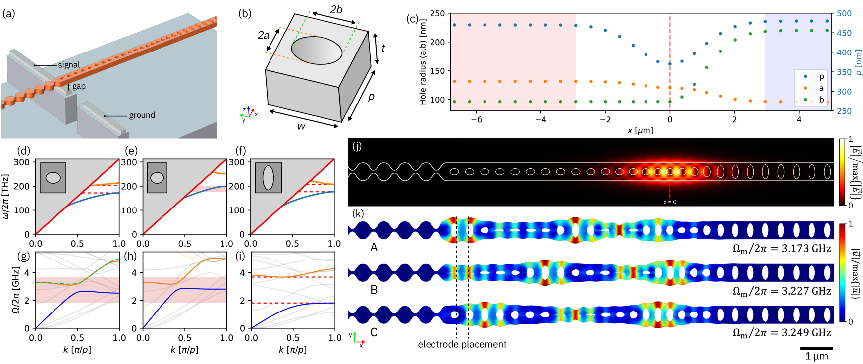
Laser light is coupled in and out of the device through a waveguide attached to it on the right side. The geometry of the optomechanical crystal cavity is adapted from the design introduced by Chan et al. [40, 44] and consists of a series of elliptical holes etched in a rectangular beam. The hole radii and pitch are however modified to create distributed mechanical modes extending between the center of the cavity and the electrode position [36]. Finite-element-method (FEM) simulations are employed to model both the photonic and phononic band structure, determine the intrinsic, radiation-limited optical quality factor, , and estimate the vacuum optomechanical coupling rate, .
The design is composed of three sections (Fig. 1(c)).
At the right end of the GaP beam (which is thick and wide), the unit cell is chosen to form a partially transparent photonic mirror with
an optical bandgap for TE-polarized light between and , where the optical coupling rate to the cavity can be controlled by varying the number of holes. This section also has a bandgap for mechanical breathing modes between and and thus serves as a phononic mirror as well.
On the left side of the device, the unit cell geometry is again chosen to create a photonic bandgap, this time between and , but now has a phonon dispersion that supports mechanical breathing modes within the phononic bandgap of the input mirror on the right side of the device.
Between these two regions, in the central portion of the beam, the unit-cell dimensions are varied to produce a confined optical mode, with the variations on each side following Gaussian functions of width . The result is a cavity supporting a localized optical mode (Fig. 1( j)) at with
.
Crucially, the dispersion of the mechanical breathing modes is nearly identical
at the center of the cavity
and on the left side of the device (see the dashed green line in Fig. 1(g)), resulting in an impedance-matched phononic waveguide.
The device is terminated on the left with a phononic reflector exhibiting a complete bandgap between and , implemented as a crenulation of the nanobeam.
This reflector, in combination with the phononic mirror on the right side of the device, forms a Fabry-Pérot-like cavity for mechanical breathing modes.
Examples of the mechanical breathing modes are shown in Fig. 1(k), the frequencies and estimated vacuum optomechanical coupling rates of which are given in Table 1.
Because the mechanical breathing modes extend along the beam, they can be directly actuated by electrodes that are spatially separated from the localized optical mode.
| Simulated | Measured | ||||||||
| Mode | [kHz] | [kHz] | |||||||
| [GHz] | [kHz] | [mHz] | [GHz] | (blue detuned) | (red detuned) | [mHz] | [rad] | ||
| A | 3.173 | 173 | 6.20 | 3.280 | 1288 | 193 | 189 | 2.32 | 0 |
| B | 3.227 | 381 | 8.02 | 3.314 | 1180 | 285 | 281 | 3.80 | |
| C | 3.249 | 506 | 25.2 | 3.328 | 1301 | 294 | 291 | 1.75 | 0 |
Fabrication
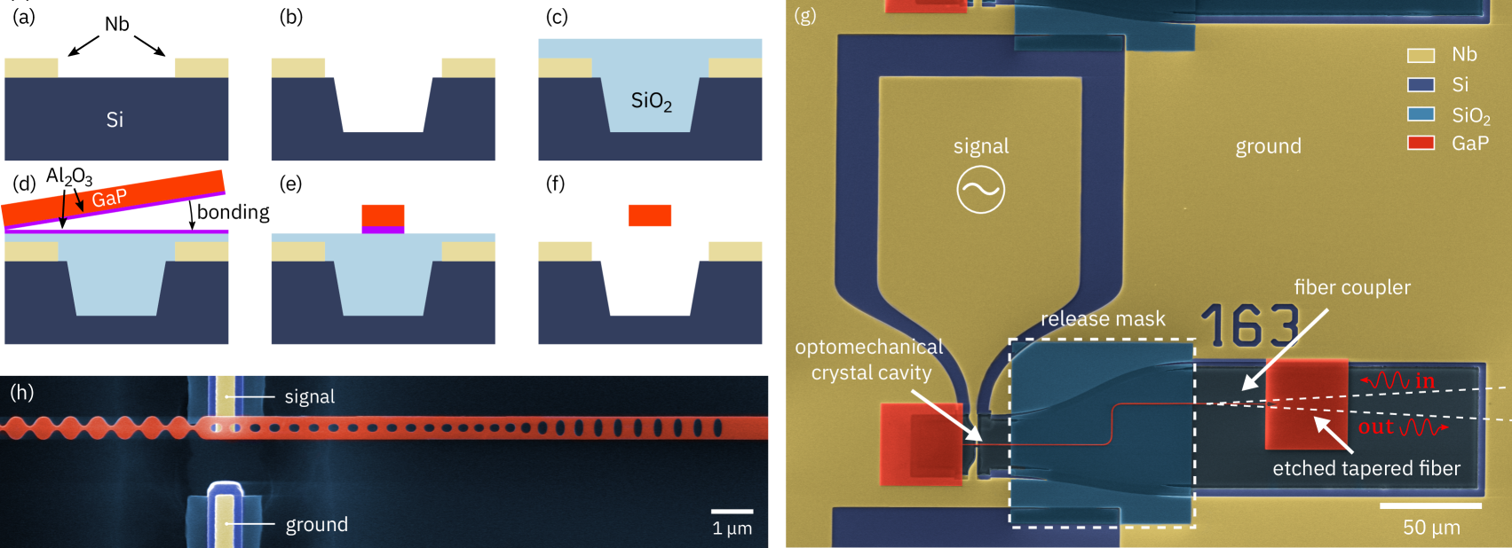
Device fabrication makes use of the processes described in our previous work on integrated GaP photonics [41, 45], with the important distinction that GaP is not bonded onto an oxidized silicon wafer but instead onto a pre-fabricated microwave circuit. The process flow is illustrated in Fig. 2. First, a -thick niobium film is deposited on a intrinsic silicon wafer by magnetron sputtering and patterned by chlorine-based dry etching into electrode structures. The vicinity of the photonic crystal cavity is then recessed by dry etching of the silicon with a HBr/O2 mixture to minimize optical losses to the substrate. The wafer is then covered with a sacrificial SiO2 layer and the surface planarized for bonding of GaP. The thickness of the SiO2 layer determines the eventual gap () between the GaP beam and the underlying niobium electrode. After dicing into chips, the GaP device layer is patterned by electron-beam lithography to form the photonic crystal cavity and the attached waveguide, which has a tapered end for adiabatic coupling to a fiber with a tapered tip formed by etching. The freestanding portion of the device is defined photolithographically and released by removal of the sacrificial SiO2 layer with buffered HF. Finally, the entire chip is coated with of Al2O3 to protect the surface and prevent photooxidation during measurement. Further details, including a description of the adiabatic fiber coupling to the device, are given in the Supplementary Information.
Optomechanical Characterization
The optical cavity mode is first interrogated in reflection with a tunable diode laser at low power () to determine the resonance frequency and the loaded quality factor .
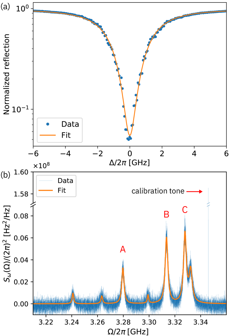
For a Lorentzian resonance, reflection from the cavity as a function of detuning with respect to the laser frequency is described by
| (1) |
where is the intrinsic cavity decay rate and is the external coupling rate [33]. A fit to Eq. 1 of the resonance observed at (Fig. 3(a)) gives a loaded optical quality factor . The coupling factor is , yielding an intrinsic quality factor . Similar values have been achieved with GaP optomechanical crystal cavities reported in other work [41, 42]. In addition to surface roughness and fabrication imperfections, absorption in the bulk of the GaP or at the surface may be limiting the intrinsic quality factor. We also find an optical mode frequency that is higher than expected from simulations, which we attribute to small deviations from the design geometry.
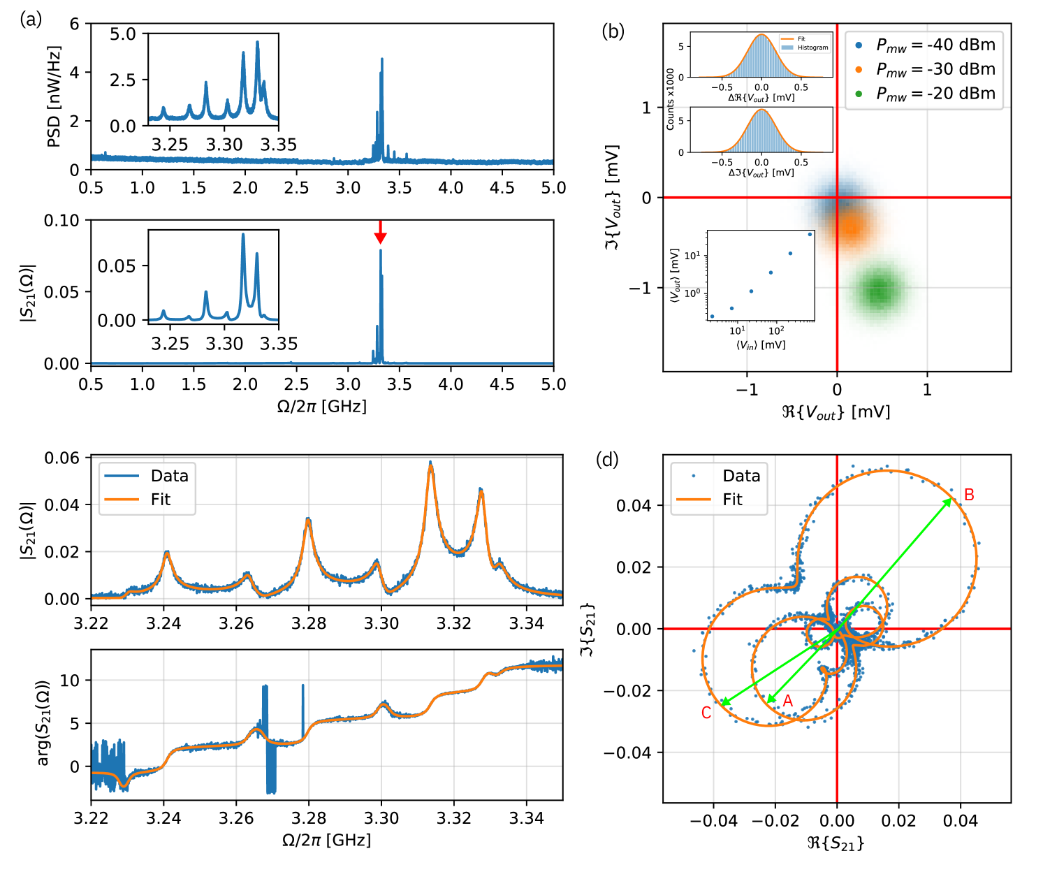
Thermally driven mechanical motion of the photonic crystal cavity modulates the cavity resonance frequency, which, for a detuned probe laser, produces amplitude fluctuations in the reflected light. We measure the resulting thermo-mechanical spectrum by direct detection with a fast photoreceiver. At frequencies above , the only modes with appreciable optomechanical coupling are observed in a narrow band between and (Fig. 3 (b) and Fig. 5(a)), in good agreement with the simulated mechanical breathing modes. As the total optical decay rate is measured to be , the system is narrowly in the resolved-sideband regime.
The vacuum optomechanical coupling rate of individual modes was determined via noise calibration [46]. To that end, the thermo-mechanical spectrum is measured at low cooperativity (, where is the mechanical damping rate and is the average number of photons in the cavity), so that effects due to dynamical backaction can be neglected. A reference signal generated by a phase modulator is added close to the mechanical modes to calibrate the spectrum. The modulation depth (where is the amplitude of the radio-frequency voltage applied to the modulator and is the half-wave voltage) at frequency is determined from the first sideband ratio (see Supplementary Information). The vacuum optomechanical coupling rate is then calculated as [46]
| (2) |
where is the average thermal occupation of the mode, is the symmetrized voltage noise spectral density produced by the photoreceiver, is the mechanical damping rate, and is the effective noise bandwidth of the spectrum analyzer’s filter function. We fit the mechanical noise spectrum with a sum of Lorentzians, as each mode produces a voltage noise spectral density that is uncorrelated with the other modes.
The device exhibits appreciable optomechanical coupling () for three modes in the frequency range ascribed to the breathing modes, which we tentatively assign to the modes depicted in Fig. 1(k). The observed mechanical resonance frequencies and coupling rates are listed in Table 1. We attribute the higher frequency of the experimentally observed modes to the Al2O3 protective coating, which increases the stiffness of the nanobeam (see Supplementary Information). The noise calibration measurement was carried out at blue and red laser detuning; the coupling rates for blue detuning are slightly higher than for red detuning, consistent with a small contribution from residual dynamical backaction.
Piezoelectric Coupling
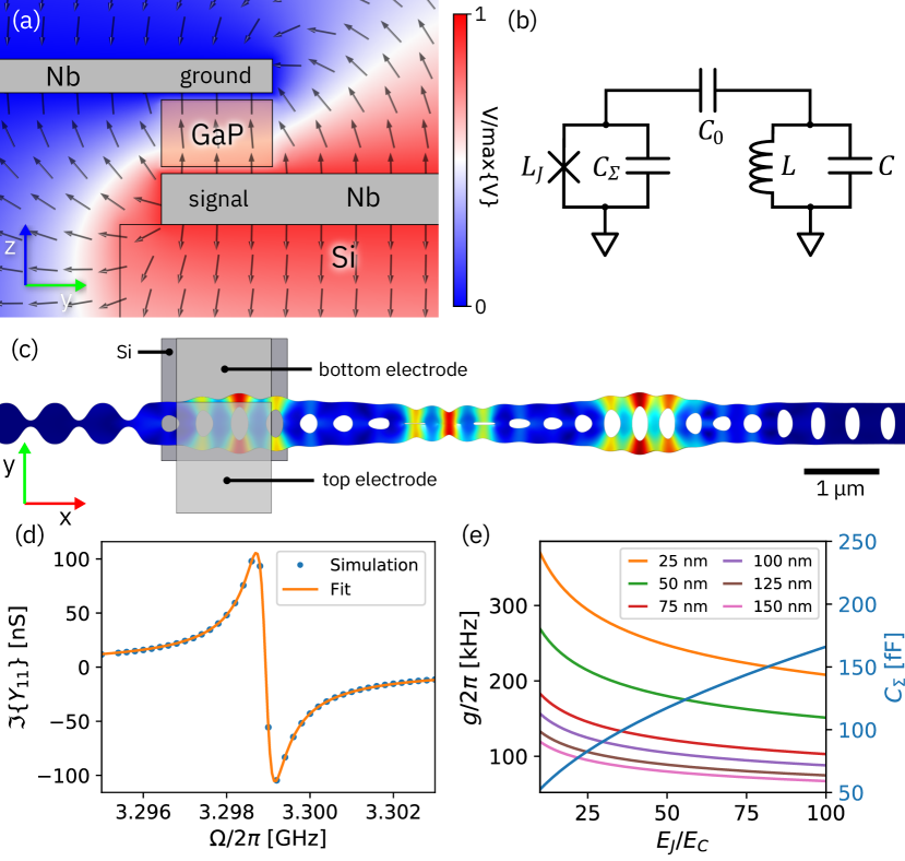
We now turn the focus of the discussion to piezoelectrically mediated actuation of the optomechanical cavity and analyze the frequency dependence of the coupling with a multiphysics FEM simulation in which the signal voltage is applied to the electrode directly under the GaP beam and the other electrode is ground (Fig. 4). The zinc-blende crystal structure of GaP dictates that mechanical breathing modes are most effectively actuated with the axis of the optomechanical crystal cavity aligned with the direction of the GaP crystal lattice and the electric field oriented along the direction (z-axis in Fig. 4). As can be seen from Fig. 4(a), the electric field for our coplanar electrode geometry has a component along the z-axis but is in general oriented at an angle. The coplanar electrode arrangement simplifies fabrication but is clearly not ideal. An optimized geometry is discussed below.
The admittance of the device as a function of frequency is calculated and fit to that of an equivalent network consisting of a series of parallel LC resonators [47] (Fig. 4 (e)). A small imaginary part is introduced to the elasticity tensor of GaP to broaden the spectral response of the individual modes and permit a coarser sampling of the spectrum. The resulting added loss is modeled as parallel resistors in the LC elements. The imaginary part of the admittance is shown in Fig. 4 (d) along with the fit to the LC network, where the electrostatic contribution of the coupling capacitor (which is determined by the geometry and dominates the admittance) has been subtracted for clarity. We find that the equivalent network provides an accurate representation of the electromechanical coupling.
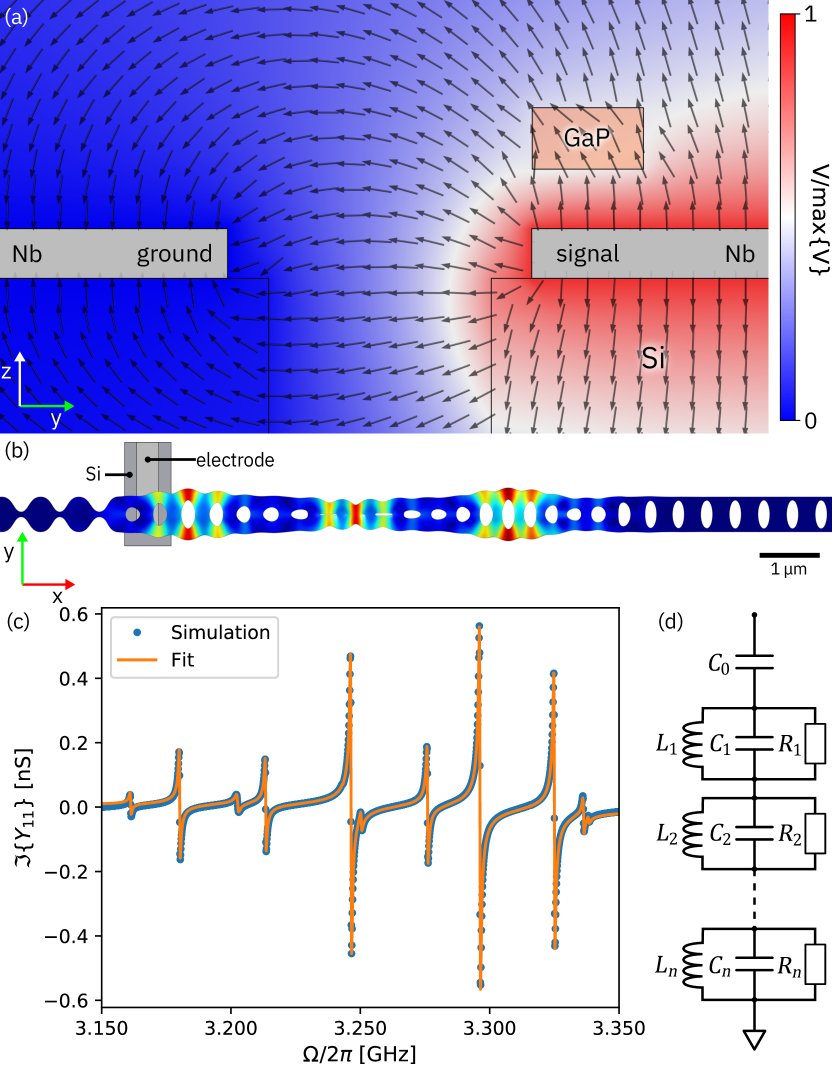
With an equivalent circuit model in place, we can estimate the coupling of each mechanical mode to the microwave probe used experimentally by employing a semi-infinite transmission-line model. Specifically, the coupling capacitor is assumed to be connected to a load impedance , yielding for the -th mode an electromechanical coupling rate of
| (3) |
with (see Supplementary Information for details). The values simulated for with a coupling capacitance of are listed in Table 1.
Microwave-to-Optical Transduction
We demonstrate microwave-to-optical transduction by driving the electrode below the device with a vector network analyzer (VNA) and measuring the optical signal from a detuned pump laser reflected from the cavity. The optomechanically induced modulation is observed by direct detection with a fast photoreceiver. The results are shown in Fig. 5. We evaluate the microwave-to-optical transduction by considering the system as a two-port network in which port 1 is the microwave probe and port 2 the photoreceiver. The scattering parameter as a function of the VNA frequency is then given by
| (4) | ||||
as derived in the Supplementary Information. Here, denotes a detection gain factor that is determined by the optical pump power, the photoreceiver’s quantum efficiency, as well as all electrical and optical loss and gain in the system. The subscript denotes the parameters for the n-th mechanical mode. The mechanical susceptibility is
| (5) |
with the mechanical damping rate and eigenfrequency . The signal delay through the cables and optical fiber is described by a frequency dependent phase offset , where is the propagation time through the signal path and is a fixed arbitrary phase offset. Additionally, there is a mode-dependent phase offset , corresponding to the relative phase difference between the mechanical displacement at the electromechanical and the optomechanical coupling positions. The optomechanically induced phase modulation is transduced into amplitude modulation detected by the photoreceiver according to the function
| (6) | ||||
where
| (7) |
is the optical susceptibility. The measured microwave-to-optical transmission amplitude is shown in Fig. 5(a), along with the thermo-mechanical spectrum for comparison. The clear correspondence between the spectra indicates that the transduction is indeed mechanically mediated.
We verify the phase-coherence of the transduced signal by recording the distribution of the photoreceiver output voltage at a fixed frequency of (where the highest transmission magnitude was observed), as displayed in Fig. 5(b). The symmetric Gaussian distribution, which is dominated by thermo-mechanical noise, and the linear dependence on microwave input power of the displacement in phase space at constant phase confirm that the transduction is linear and coherent.
The amplitude and phase of the transmission spectrum in the relevant range from to are shown in Fig. 5(c) together with a fit to Eq. 4. The phase-space representation of the same data (Fig. 5(d)), exhibits circular curves characteristic of harmonic oscillators. The fit makes use of a separate calibration of the optical cavity response to determine , performed by phase-modulating the optical pump with a pre-determined modulation depth (see Supplementary Information). Using the previously measured vacuum optomechanical coupling rates, the electromechanical coupling rate is then determined from the microwave-to-optical transmission. The fit results for the three mechanical modes with the strongest transduction, which we assign to modes A, B, and C, are shown in Table 1.
Concerning the observed mode-dependent phase offset in the signal that we fix at either or , we understand this phenomenon to be a result of the shape of each breathing mode’s displacement field. When a mode is driven coherently, the mechanical displacement field in the portion of the GaP beam that overlaps with the electrode inherits its relative phase from the microwave drive. The optical mode however couples to a different region that might be in phase or out of phase by with respect to the piezoelectrically coupled region (see Fig. 1(k)). Consequently, the optomechanically induced phase modulation of the optical field may also have an added phase offset of (modes A and C) or (mode B) with respect to the microwave drive. Note that, although the device possesses several other breathing modes, only the three modes A, B, and C provide a reasonable qualitative agreement between simulations and experiment with respect to mechanical frequency, optomechanical coupling rate, and mode-dependent phase offset, justifying the assignment.
Outlook: Coupling to a Transmon Qubit
In addition to transmission line coupling, we also estimated the expected electromechanical coupling rate to a superconducting transmon qubit. We restrict the discussion here to an optimized configuration with one electrode below and the other above the photonic crystal cavity with equal gaps to the electrodes (Fig. 6(a)). The capacitive qubit-resonator coupling scheme is depicted in Fig. 6(b), with the circuit parameters , and extracted from an admittance fit similar to that described above. In this case, we simulate only the admittance of mechanical mode C, as it exhibits the highest simulated electromechanical coupling in the coplanar geometry. The bilinear coupling between the qubit and the resonator is given by
| (8) |
where is the qubit shunt capacitance, and the first qubit transition frequency is (see Supplementary Information for details). For optimal coupling, we assume that the qubit is tuned into resonance with the mechanical oscillator, i.e., . The estimated coupling rate is shown in Fig. 6(e) for various gap sizes between the electrodes and the optomechanical crystal cavity as a function of the ratio of Josephson energy to charging energy of the qubit . For the qubit to exhibit low charge dispersion, a ratio is required [48]. For a gap to the electrodes of , which can be realistically fabricated, we calculate a coupling rate of for , well within the transmon regime, with . Previously, mechanical quality factors of have been reported for similar GaP optomechanical crystal cavities at the cryogenic temperature required for single phonon manipulation [42], which corresponds at to a mechanical damping rate of . We therefore estimate that the system presented here would be deep enough in the strong coupling regime to permit a faithful swap of the qubit and mechanical resonator states, if the qubit lifetime . Given the small contribution of the piezoelectric portion () to the total capacitance of such a system, we expect this to be achievable with current technology.
Conclusion
In summary, we have presented a novel platform for microwave-to-optical conversion based on single-crystal GaP optomechanical devices integrated directly on pre-fabricated niobium-on-silicon electrode structures. The extended mechanical breathing modes of our optomechanical crystal cavities were designed for both high optomechanical coupling rates (up to ) and piezoelectric actuation by the microwave electrodes. Despite the asymmetric cavity structure and the close proximity of the metal electrodes, high optical quality factors () were obtained, placing the system in the resolved-sideband regime (). Coherent microwave-to-optical transduction in a transmission-line coupled device was demonstrated. The electromechanical coupling rates observed experimentally were substantially smaller than expected from simulations. The discrepancy could be fabrication-related or may be due to insufficient knowledge of the piezoelectric properties of GaP. In future experiments, we aim to integrate the cavity design presented here with superconducting transmon qubits, for which our simulations indicate that strong coupling can be achieved (). Due to the small participation ratio of the device in the overall qubit energy, we expect long qubit lifetimes.
Acknowledgements
We gratefully acknowledge Katharina Schmeing, Yannick Baumgartner, Lukas Czornomaz, Ute Drechsler, Diana Davila and Antonis Olziersky for their valuable contributions to development of the GaP-on-insulator platform. We also thank Darius Urbonas, Matthias Mergenthaler, Thomas Karg and Charles Möhl for useful discussios. This work was supported by the European Union’s Horizon 2020 Program for Research and Innovation under grant agreement No. 722923 (Marie Curie H2020-ETN OMT) and No. 732894 (FET Proactive HOT). All samples were fabricated at the Binnig and Rohrer Nanotechnology Center (BRNC) at IBM Research Europe, Zurich.
Contributions
S.H. designed the device and carried out the epitaxial growth of GaP as well as the microfabrication processes. S.H. performed FEM simulations of the photonic crystal cavities with support from A.B.. Wafer bonding of GaP was done by D.C.. Y.P. carried out chemical mechanical polishing with support from S.H.. P.S. conceived and oversaw the project.
References
- Arute et al. [2019] F. Arute, K. Arya, R. Babbush, D. Bacon, J. C. Bardin, R. Barends, R. Biswas, S. Boixo, F. G. Brandao, D. A. Buell, et al., Nature 574, 505 (2019).
- Jurcevic et al. [2021] P. Jurcevic, A. Javadi-Abhari, L. S. Bishop, I. Lauer, D. F. Bogorin, M. Brink, L. Capelluto, O. Günlük, T. Itoko, N. Kanazawa, et al., Quantum Science and Technology 6, 025020 (2021).
- Cirac et al. [1997] J. I. Cirac, P. Zoller, H. J. Kimble, and H. Mabuchi, Physical Review Letters 78, 3221 (1997).
- Duan et al. [2001] L.-M. Duan, M. D. Lukin, J. I. Cirac, and P. Zoller, Nature 414, 413 (2001).
- Kimble [2008] H. J. Kimble, Nature 453, 1023 (2008).
- Magnard et al. [2020] P. Magnard, S. Storz, P. Kurpiers, J. Schär, F. Marxer, J. Lütolf, T. Walter, J.-C. Besse, M. Gabureac, K. Reuer, et al., Physical Review Letters 125, 260502 (2020).
- Landry et al. [2007] O. Landry, J. A. W. van Houwelingen, A. Beveratos, H. Zbinden, and N. Gisin, JOSA B 24, 398 (2007).
- Lauk et al. [2020] N. Lauk, N. Sinclair, S. Barzanjeh, J. P. Covey, M. Saffman, M. Spiropulu, and C. Simon, Quantum Science and Technology 5, 020501 (2020).
- Lambert et al. [2020] N. J. Lambert, A. Rueda, F. Sedlmeir, and H. G. Schwefel, Advanced Quantum Technologies 3, 1900077 (2020).
- Zhong et al. [2020] C. Zhong, Z. Wang, C. Zou, M. Zhang, X. Han, W. Fu, M. Xu, S. Shankar, M. H. Devoret, H. X. Tang, et al., Physical review letters 124, 010511 (2020).
- Rueda et al. [2019] A. Rueda, W. Hease, S. Barzanjeh, and J. M. Fink, npj Quantum Information 5, 1 (2019).
- Soltani et al. [2017] M. Soltani, M. Zhang, C. Ryan, G. J. Ribeill, C. Wang, and M. Loncar, Physical Review A 96, 043808 (2017).
- Rueda et al. [2016] A. Rueda, F. Sedlmeir, M. C. Collodo, U. Vogl, B. Stiller, G. Schunk, D. V. Strekalov, C. Marquardt, J. M. Fink, O. Painter, et al., Optica 3, 597 (2016).
- Fan et al. [2018] L. Fan, C.-L. Zou, R. Cheng, X. Guo, X. Han, Z. Gong, S. Wang, and H. X. Tang, Science advances 4, eaar4994 (2018).
- Witmer et al. [2020] J. D. Witmer, T. P. McKenna, P. Arrangoiz-Arriola, R. Van Laer, E. A. Wollack, F. Lin, A. K. Jen, J. Luo, and A. H. Safavi-Naeini, Quantum Science and Technology 5, 034004 (2020).
- Javerzac-Galy et al. [2016] C. Javerzac-Galy, K. Plekhanov, N. Bernier, L. D. Toth, A. K. Feofanov, and T. J. Kippenberg, Physical Review A 94, 053815 (2016).
- Hisatomi et al. [2016] R. Hisatomi, A. Osada, Y. Tabuchi, T. Ishikawa, A. Noguchi, R. Yamazaki, K. Usami, and Y. Nakamura, Physical Review B 93, 174427 (2016).
- Vogt et al. [2019] T. Vogt, C. Gross, J. Han, S. B. Pal, M. Lam, M. Kiffner, and W. Li, Physical Review A 99, 023832 (2019).
- Han et al. [2018] J. Han, T. Vogt, C. Gross, D. Jaksch, M. Kiffner, and W. Li, Physical review letters 120, 093201 (2018).
- Bartholomew et al. [2020] J. G. Bartholomew, J. Rochman, T. Xie, J. M. Kindem, A. Ruskuc, I. Craiciu, M. Lei, and A. Faraon, Nature Communications 11, 1 (2020).
- Everts et al. [2019] J. R. Everts, M. C. Berrington, R. L. Ahlefeldt, and J. J. Longdell, Physical Review A 99, 063830 (2019).
- Williamson et al. [2014] L. A. Williamson, Y.-H. Chen, and J. J. Longdell, Physical review letters 113, 203601 (2014).
- Tsang [2010] M. Tsang, Physical Review A 81, 063837 (2010).
- Tsang [2011] M. Tsang, Physical Review A 84, 043845 (2011).
- Andrews et al. [2014] R. W. Andrews, R. W. Peterson, T. P. Purdy, K. Cicak, R. W. Simmonds, C. A. Regal, and K. W. Lehnert, Nature Physics 10, 321 (2014).
- Bagci et al. [2014] T. Bagci, A. Simonsen, S. Schmid, L. G. Villanueva, E. Zeuthen, J. Appel, J. M. Taylor, A. Sørensen, K. Usami, A. Schliesser, et al., Nature 507, 81 (2014).
- Higginbotham et al. [2018] A. P. Higginbotham, P. Burns, M. Urmey, R. Peterson, N. Kampel, B. Brubaker, G. Smith, K. Lehnert, and C. Regal, Nature Physics 14, 1038 (2018).
- Jiang et al. [2020] W. Jiang, C. J. Sarabalis, Y. D. Dahmani, R. N. Patel, F. M. Mayor, T. P. McKenna, R. Van Laer, and A. H. Safavi-Naeini, Nature Communications 11, 1 (2020).
- Balram et al. [2016] K. C. Balram, M. I. Davanço, J. D. Song, and K. Srinivasan, Nature Photonics 10, 346 (2016).
- Vainsencher et al. [2016] A. Vainsencher, K. Satzinger, G. Peairs, and A. Cleland, Applied Physics Letters 109, 033107 (2016).
- Bochmann et al. [2013] J. Bochmann, A. Vainsencher, D. D. Awschalom, and A. N. Cleland, Nature Physics 9, 712 (2013).
- Shao et al. [2019] L. Shao, M. Yu, S. Maity, N. Sinclair, L. Zheng, C. Chia, A. Shams-Ansari, C. Wang, M. Zhang, K. Lai, et al., Optica 6, 1498 (2019).
- Aspelmeyer et al. [2014] M. Aspelmeyer, T. J. Kippenberg, and F. Marquardt, Reviews of Modern Physics 86, 1391 (2014).
- Riedinger et al. [2016] R. Riedinger, S. Hong, R. A. Norte, J. A. Slater, J. Shang, A. G. Krause, V. Anant, M. Aspelmeyer, and S. Gröblacher, Nature 530, 313 (2016).
- Riedinger et al. [2018] R. Riedinger, A. Wallucks, I. Marinković, C. Löschnauer, M. Aspelmeyer, S. Hong, and S. Gröblacher, Nature 556, 473 (2018).
- Mirhosseini et al. [2020] M. Mirhosseini, A. Sipahigil, M. Kalaee, and O. Painter, Nature 588, 599 (2020).
- Chu et al. [2018] Y. Chu, P. Kharel, T. Yoon, L. Frunzio, P. T. Rakich, and R. J. Schoelkopf, Nature 563, 666 (2018).
- Satzinger et al. [2018] K. J. Satzinger, Y. Zhong, H.-S. Chang, G. A. Peairs, A. Bienfait, M.-H. Chou, A. Cleland, C. R. Conner, É. Dumur, J. Grebel, et al., Nature 563, 661 (2018).
- Arrangoiz-Arriola et al. [2019] P. Arrangoiz-Arriola, E. A. Wollack, Z. Wang, M. Pechal, W. Jiang, T. P. McKenna, J. D. Witmer, R. Van Laer, and A. H. Safavi-Naeini, Nature 571, 537 (2019).
- Chan et al. [2011] J. Chan, T. M. Alegre, A. H. Safavi-Naeini, J. T. Hill, A. Krause, S. Gröblacher, M. Aspelmeyer, and O. Painter, Nature 478, 89 (2011).
- Schneider et al. [2019] K. Schneider, Y. Baumgartner, S. Hönl, P. Welter, H. Hahn, D. J. Wilson, L. Czornomaz, and P. Seidler, Optica 6, 577 (2019).
- Stockill et al. [2019] R. Stockill, M. Forsch, G. Beaudoin, K. Pantzas, I. Sagnes, R. Braive, and S. Gröblacher, Physical review letters 123, 163602 (2019).
- Forsch et al. [2020] M. Forsch, R. Stockill, A. Wallucks, I. Marinković, C. Gärtner, R. A. Norte, F. van Otten, A. Fiore, K. Srinivasan, and S. Gröblacher, Nature Physics 16, 69 (2020).
- Chan et al. [2012] J. Chan, A. H. Safavi-Naeini, J. T. Hill, S. Meenehan, and O. Painter, Applied Physics Letters 101, 081115 (2012).
- Wilson et al. [2020] D. J. Wilson, K. Schneider, S. Hönl, M. Anderson, Y. Baumgartner, L. Czornomaz, T. J. Kippenberg, and P. Seidler, Nature Photonics 14, 57 (2020).
- Gorodetksy et al. [2010] M. Gorodetksy, A. Schliesser, G. Anetsberger, S. Deleglise, and T. J. Kippenberg, Optics express 18, 23236 (2010).
- Arrangoiz-Arriola and Safavi-Naeini [2016] P. Arrangoiz-Arriola and A. H. Safavi-Naeini, Physical Review A 94, 063864 (2016).
- Koch et al. [2007] J. Koch, M. Y. Terri, J. Gambetta, A. A. Houck, D. Schuster, J. Majer, A. Blais, M. H. Devoret, S. M. Girvin, and R. J. Schoelkopf, Physical Review A 76, 042319 (2007).