Generation of Spin Defects by Ion Implantation in Hexagonal Boron Nitride
Abstract
Abstract: Optically addressable spin defects in wide band gap semiconductors as promising systems for quantum information and sensing applications have recently attracted increasing attention. Spin defects in two-dimensional materials are expected to show superiority in quantum sensing due to their atomic thickness. Here, we demonstrate that an ensemble of negatively charged boron vacancy (V) with good spin properties in hexagonal boron nitride can be generated by ion implantation. We carry out optically detected magnetic resonance measurements at room temperature to characterize the spin properties of ensembles of V defects, showing a zero-field splitting frequency of 3.47 GHz. We compare the photoluminescence intensity and spin properties of V defects generated using different implantation parameters, such as fluence, energy and ion species. With the use of proper parameters, we can successfully create V defects with high probability. Our results provide a simple and practicable method to create spin defects in hBN, which is of great significance for realizing integrated hBN-based devices.
Keywords: 2D materials, hexagonal boron nitride, negatively charged boron vacancy, spin properties, ion implantation
pacs:
78.67.Hc, 42.50.-p, 78.55.-mI INTRODUCTION
Solid-state spin defects have attracted widespread attention as promising quantum systems in recent decades awschalom2013quantum and have numerous applications in quantum information togan2010quantum ; waldherr2014quantum and quantum sensing maze2008nanoscale ; kolkowitz2012coherent . Some prominent systems have been studied extensively, including the nitrogen vacancy (NV) center gali2019ab ; plakhotnik2014all ; stanwix2010coherence ; wang2016coherence and the silicon vacancy center becker2018all ; rogers2014all in diamond and the divacancy center li2020room ; seo2016quantum and silicon vacancy center dong2019spin ; carter2015spin in silicon carbide. Although these defects have many remarkable properties, such as a long spin coherence time at room temperature balasubramanian2009ultralong , there are some intrinsic limitations due to the three-dimensional nature of the materials. For example, it is difficult to prepare spin defects close to the sample surface, which affects the sensitivity of the sensor zhang2017depth .
Recently, the emergence of spin defects in two-dimensional materials and van der Waals crystals has provided a remedy for the limitations of three-dimensional materials. One of the outstanding materials is hexagonal boron nitride (hBN), which possesses a wide bandgap and a variety of atom-like defects, making hBN a good quantum system for single-photon emitters xia2019room ; tran2016robust ; li2019purification ; camphausen2020observation ; bourrellier2016bright ; mendelson2021identifying ; Stern2021 and spin-addressable systems mendelson2021identifying ; Stern2021 ; gottscholl2020initialization ; gottscholl2021room ; liu2021rabi at room temperature. Currently, most studies of spin defects are focused on the negatively charged boron vacancy (V) that consists of a missing boron atom replaced by an extra electron in the hBN crystal gottscholl2020initialization ; kianinia2020generation ; gao2020femtosecond ; gottscholl2021room ; liu2021rabi ; liu2021temperature ; gottscholl2021sub ; murzakhanov2021creation ; abdi2018color ; Ivady2020 ; Sajid2020 . The V defects are photostable and exhibit good spin properties at room temperature gottscholl2020initialization . In addition, the V defects have a triplet ground state (S = 1) and can be initialized, manipulated and optically read out at room temperature, showing the potential for spin-based quantum information and sensing applications gottscholl2021room ; gottscholl2020initialization .
In this context, we demonstrate a new way to generate V defects in hBN crystals by an ion implantation process using an ion implanter. At present, V defects can be generated by high-dose neutron irradiation gottscholl2020initialization , focused ion beam (FIB) implantation kianinia2020generation , femtosecond laser writing gao2020femtosecond , and high-energy electron irradiation murzakhanov2021creation . With appropriate energy and fluence for implanted ions, we successfully created ensembles of V defects using an ion implanter, which exhibit good contrast in optically detected magnetic resonance (ODMR) results. In addition, we measured the Rabi oscillations and spin-lattice relaxation time () of the defects (see Supporting Information).
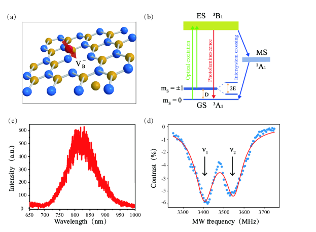
In the experiment, we used a commercially available monocrystalline hBN sample purchased from HQ Graphene with a lateral size of 1 mm. Monocrystalline hBN is exfoliated with tape into 10100 nm-thick flakes, which are later transferred onto a silicon substrate. The sample is then put into an ion implanter (IonImplantatation-CETC-M56100) and the hBN flakes are implanted with parallelized ion beams over a large area. Through the ion implantation process we successfully created V defects. The process is schematically shown in Figure 1a. The high-energy ions break the B-N bonds in the hBN lattice and knock out boron atoms, leaving behind negatively charged vacancies. The photoluminescence (PL) and spin properties of the defects were characterized by using a confocal microscope system combined with a microwave system. We used a 532-nm laser to excite the defects with a laser power of 4.7 mW, a 0.5 N.A. objective (Olympus) to focus onto the sample and collect the fluorescence utilizing a 9-m-core-diameter fiber attached to an avalanche photodiode, and a copper wire with a diameter of 20 m placed close to the implanted sample as an antenna to deliver a microwave field liu2021temperature ; wang2019demand .
II RESULTS AND DISCUSSION
With the setup described above, we first characterized the PL spectrum of an ensemble of defects generated by implanting nitrogen ions with an energy of 30 keV and a fluence of 1 10 ions/cm, as shown in Figure 1c. The implanted samples exhibit strong PL emission ranging from 700 nm to 1000 nm and a center at approximately 820 nm, which is the characteristic of V centers and consistent with reported V defects created by neutron irradiation, FIB and laser writing gottscholl2020initialization ; kianinia2020generation ; gao2020femtosecond . In addition, the V defects that we create are stable for an extented period of time at room temperature (see Supporting Information).
To further verify that the ensemble of defects generated by ion implantation are V centers, we performed optically detected magnetic resonance (ODMR) measurements at room temperature. ODMR measurements were carried out by scanning the frequency of the microwave field from 3250 MHz to 3750 MHz without an external magnetic field and the ODMR spectrum was fitted by a two-Lorentzian function, as shown in Figure 1d. The result indicates that the fluorescence signal drops when the microwave field oscillates at 3405 MHz and 3548 MHz, which is consistent with the ODMR spectra measured for V defects in previous works gottscholl2020initialization ; liu2021temperature . Figure 1b shows that the excited state of the V center is more likely to return to the ground state through nonradiative intersystem crossing, so the V spin will be polarized into the ground state under continuous laser excitation. When the microwave frequency is in resonance with the split between the ground state sublevels, electrons in the state will be pumped into the state, leading to a decrease in fluorescence intensity liu2021temperature . The V center has a triplet ground state () with a zero-field splitting (ZFS) described by the parameters and . The resonance frequencies and in the ODMR spectrum can be represented by , where is the Planck constant, is the Land factor, is the Bohr magneton and is the static magnetic field gottscholl2020initialization . In the absence of external magnetic field, the ZFS parameters and are given by and . In our experiment, we find MHz and MHz. The V defects exhibit a good ODMR contrast (up to 22%, see Supporting Information) and a long relaxation time (up to 17 s, see Supporting Information) at room temperature, which shows promising spin properties for V defects generated by ion implantation.
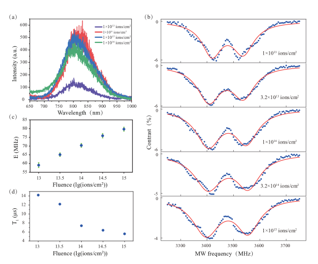
Next, we studied the effect of different implantation parameters, such as implantation fluence, energy and ion species. First, we compared the implantation effect of different fluences. We generated defects by implanting nitrogen ions with the same energy (30 keV) and increasing fluence from 1 10 to 1 10 ions/cm. Figure 2a shows a comparison of the room temperature PL spectra for four defect samples. We find that the intensity of the PL spectra increases with increasing fluence at low doses. When the fluence is increased up to 1 10 ions/cm, the PL intensity is shown to decrease slightly, which is similar to that observed for V defects in silicon carbide and NV and SiV centers in diamond wang2019demand ; schwartz2011situ ; schroder2017scalable . This decrease can be considered a saturation phenomenon for the V defects generated by ion implantation, which might result from the ion-induced damage of the crystal lattices that accumulates in the form of multiple vacancy defects wang2019demand ; schwartz2011situ ; schroder2017scalable . The ODMR spectra with two-Lorentzian fitting at different fluences are shown in Figure 2b. The measurements were carried out without an external magnetic field at room temperature. We find that the ZFS parameter is stable at 3475 MHz (see Supporting Information), while the ZFS parameter increases almost linearly with the fluence ranging from 1 10 to 1 10 ions/cm, as shown in Figure 2c. Nevertheless, when the fluence reaches to 1 10 ions/cm, the ZFS parameter is no longer stable and varies from 3460 MHz to 3520 MHz, and is no longer linear (see Supporting Information). Furthermore, we measured the spin-lattice relaxation times of the defects, as shown in Figure 2d, which was found to be negatively correlated with the implantation fluence. The dependence of and on fluence can be attributed to the increasing crystal damage with fluence. Damage due to ion implantation can give rise to local strain fields vanDam2019Optical , which has an effect on electron spin transitions. The strain field in hBN is mainly manifested as transverse strain when the damage is not very large Jin2009Fabrication ; Feng2018Imaging , and the effect of transverse strain, as stated in Ref. Teissier2014Strain , is equivalent to a modification of . The more severe the damage, the larger the transverse strain, and then the larger the transverse splitting. Meanwhile, the damage can deteriorate the spin and optical coherence properties of defects Tetienne2018Spin , which suggests that more severe damage will lead to a shorter .
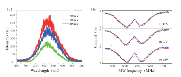
Then, to compare the implantation effect of different energies, we generated defects by implanting nitrogen ions with the same fluence (1 10 ions/cm) and varying energy from 20 keV to 40 keV. Figure 3a shows a comparison of the PL spectra measured for these defect samples, and Figure 3b shows a comparison of the ODMR spectra measured at room temperature. We can see that different energies mainly affect the PL intensity but have almost no effect on the spin properties of the V defects. The PL spectrum for the V defects generated at 30-keV energy displays higher intensity than that of V defects generated at other energies, while the ODMR spectra of the V defects generated at different energies display the same resonance frequency, i.e., the same ZFS parameters and . Additionally, we find that the spin lattice relaxation times scarcely change with the implantation energies (see Supporting Information). Because our hBN samples are 10100 nm-thick flakes, ions can easily penetrate the flakes rather than remain in the samples, even at low energy. Although the implantation energies are different, the damage due to ion implantation with the same ion species and fluence is similar. Therefore, implantation energy does not affect the spin properties of the defects.
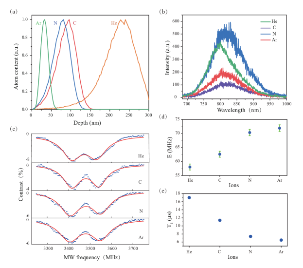
Finally, to compare the implantation effect of different ion species, we generated defects by implanting nitrogen, argon, helium and carbon ions with the same fluence (1 10 ions/cm) and energy (30 keV), respectively. We simulate the theoretical distribution of the V defects with depth created by different ions using a stopping-and-range-of-ions-in-matter (SRIM) simulation, as shown in Figure 4a. The result indicates that the number of generated defects and the penetration depth are obviously different for different ions. Argon ions are more likely to create shallow defects, while helium ions can be used to create defects in thicker samples. Figure 4b shows a comparison of the PL spectra measured for these samples at room temperature, from which we can see that the sample implanted using nitrogen ions has the highest PL intensity. Figure 4c shows the ODMR spectra for the defects generated by different implantation ions, indicating that they all have spin properties. We find that when we implant different ions, the ZFS parameter is stable at 3475 MHz (see Supporting Information), while the ZFS parameter is different, which is similar to implantation with different fluences. The difference in the ZFS parameter is shown in Figure 4d, showing that the ZFS parameter increases as the ion radius increases. Additionally, the spin-lattice relaxation times for the defects decrease as the ion radius increases, as shown in Figure 4e. Similar to the dose-dependent relationship mentioned above, the dependence of and on the ion species can also be attributed to crystal damage. With increasing atomic number, the damage increases due to the larger collision cross-section, thus, increases and decreases.
III CONCLUSIONS
We successfully generated optically active V defects by ion implantation in hBN. There are also several other ways to generate V defects, such as the neutron-irritation method, the FIB method, the laser-writing method, and the electron-irradiation method. All these methods have their own advantages and disadvantages. For example, the neutron-irritation method is the primary way to generate V defects, but it needs to be carried out in a nuclear reactor, which is not very convenient and slightly expensive. Comparatively, the ion-implantation method is convenient and inexpensive because the ion implanter is commercially available. The FIB method allows for the patterning of arrays of spin defects due to its controllability and good positioning. This is the advantage of this method. However, to the best of our knowledge, the ion source often used for commercial FIBs is Ga, and the use of other ion sources is rare. In contrast, the ion implanter has a variety of available ion sources (He+, C+, N+, Ar+, etc.), and, moreover, the ion-implantation method can be used to create V defects over a large scale. The laser-writing method is simple and flexible, as it can be conducted in an ambient environment with no vacuum requirement. However, the required femtosecond laser pulse has a relatively large energy and is possibly destructive towards the sample. In comparison, the ion-implantation method is gentle and results in little damage to the sample. In addition, the electron irradiation method makes it possible to avoid clustering of defects, but it requires very high electron energy (2 MeV). Relatively, the ion-implantation method needs only a relatively low ion energy (30 keV). Therefore, our ion-implantation method will be a good supplement to all the above-mentioned methods.
Our results show that the implantation parameters, such as fluence, energy and ion species, have clear effects on the PL intensity and spin properties of ion-implantation-generated V defects. Therefore, we can create good ensembles of V defects with high probability by adjusting the fluence (1 10 ions/cm) and energy (30 keV) of the implanted nitrogen ions, and the V defects exhibit a good ODMR contrast at room temperature, which is important for spin-addressable systems. Furthermore, we find that the defects created by implanting helium ions with an energy of 30 keV and a fluence of 1 10 ions/cm have the longest spin-lattice relaxation time of 17 microseconds at room temperature, which is comparable to that achieved for defects created by neutron irradiation liu2021rabi ; gottscholl2021room . Our work provides a simple and practicable method for controllable engineering of spin defects in hBN and paves the way for integrated quantum information and sensing applications.
Supporting Information
This material is available free of charge via the internet at xxxxxxxxxxxx.
Additional data, PL stability, and probablity of generating a V center.
Author Information
Corresponding Authors
Wei Liu - CAS Key Laboratory of Quantum Information and CAS Center For Excellence in Quantum Information and Quantum Physics, University of Science and Technology of China, Hefei 230052, People’s Republic of China; Email: lw691225@ustc.edu.cn
Yi-Tao Wang - CAS Key Laboratory of Quantum Information and CAS Center For Excellence in Quantum Information and Quantum Physics, University of Science and Technology of China, Hefei 230052, People’s Republic of China; Email: yitao@ustc.edu.cn
Jian-Shun Tang - CAS Key Laboratory of Quantum Information and CAS Center For Excellence in Quantum Information and Quantum Physics, University of Science and Technology of China, Hefei 230052, People’s Republic of China; Email: tjs@ustc.edu.cn
Chuan-Feng Li - CAS Key Laboratory of Quantum Information and CAS Center For Excellence in Quantum Information and Quantum Physics, University of Science and Technology of China, Hefei 230052, People’s Republic of China; orcid.org/0000-0001-6815-8929; Email: cfli@ ustc.edu.cn
Authors
Nai-Jie Guo - CAS Key Laboratory of Quantum Information and CAS Center For Excellence in Quantum Information and Quantum Physics, University of Science and Technology of China, Hefei 230052, People’s Republic of China; Email: guonaijie@mail.ustc.edu.cn
Zhi-Peng Li - CAS Key Laboratory of Quantum Information and CAS Center For Excellence in Quantum Information and Quantum Physics, University of Science and Technology of China, Hefei 230052, People’s Republic of China; Email: lzp0116@mail.ustc.edu.cn
Yuan-Ze Yang - CAS Key Laboratory of Quantum Information and CAS Center For Excellence in Quantum Information and Quantum Physics, University of Science and Technology of China, Hefei 230052, People’s Republic of China; Email: yyz14@mail.ustc.edu.cn
Shang Yu - CAS Key Laboratory of Quantum Information and CAS Center For Excellence in Quantum Information and Quantum Physics, University of Science and Technology of China, Hefei 230052, People’s Republic of China; Email: yushang@mail.ustc.edu.cn
Yu Meng - CAS Key Laboratory of Quantum Information and CAS Center For Excellence in Quantum Information and Quantum Physics, University of Science and Technology of China, Hefei 230052, People’s Republic of China; Email: mengyu23@mail.ustc.edu.cn
Zhao-An Wang - CAS Key Laboratory of Quantum Information and CAS Center For Excellence in Quantum Information and Quantum Physics, University of Science and Technology of China, Hefei 230052, People’s Republic of China; Email: zawang@mail.ustc.edu.cn
Xiao-Dong Zeng - CAS Key Laboratory of Quantum Information and CAS Center For Excellence in Quantum Information and Quantum Physics, University of Science and Technology of China, Hefei 230052, People’s Republic of China; Email: zengxiaodong@mail.ustc.edu.cn
Fei-Fei Yan - CAS Key Laboratory of Quantum Information and CAS Center For Excellence in Quantum Information and Quantum Physics, University of Science and Technology of China, Hefei 230052, People’s Republic of China; Email: yanff@mail.ustc.edu.cn
Qiang Li - CAS Key Laboratory of Quantum Information and CAS Center For Excellence in Quantum Information and Quantum Physics, University of Science and Technology of China, Hefei 230052, People’s Republic of China; Email: qianglee@ustc.edu.cn
Jun-Feng Wang - CAS Key Laboratory of Quantum Information and CAS Center For Excellence in Quantum Information and Quantum Physics, University of Science and Technology of China, Hefei 230052, People’s Republic of China; Email: jfwang89@ustc.edu.cn
Jin-Shi Xu - CAS Key Laboratory of Quantum Information and CAS Center For Excellence in Quantum Information and Quantum Physics, University of Science and Technology of China, Hefei 230052, People’s Republic of China; Email: jsxu@ustc.edu.cn
Guang-Can Guo - CAS Key Laboratory of Quantum Information and CAS Center For Excellence in Quantum Information and Quantum Physics, University of Science and Technology of China, Hefei 230052, People’s Republic of China; Email: gcguo@ustc.edu.cn
ACKNOWLEDGMENTS
This work was supported by the National Key Research and Development Program of China (No. 2017YFA0304100), the National Natural Science Foundation of China (Grants Nos. 12174370, 11822408, 12174376, 11774335, 11821404, and 11904356), the Open Research Projects of Zhejiang Lab (NO. 2021MB0AB02), the Key Research Program of Frontier Sciences of the Chinese Academy of Sciences (Grant No. QYZDY-SSW-SLH003), the Fok Ying-Tong Education Foundation (No. 171007), Science Foundation of the CAS (No. ZDRW-XH-2019-1), Anhui Initiative in Quantum Information Technologies (AHY020100, AHY060300), the Fundamental Research Funds for the Central Universities (Nos. WK2470000026, WK2030000008 and WK2470000028). This work was partially carried out at the USTC Center for Micro and Nanoscale Research and Fabrication.
References
- (1) Awschalom, D. D.; Bassett, L. C.; Dzurak, A. S.; Hu, E. L.; Petta, J. R. Quantum spintronics: engineering and manipulating atom-like spins in semiconductors. Science 2013, 339, 1174-1179.
- (2) Togan, E.; Chu, Y.; Trifonov, A. S.; Jiang, L.; Maze, J.; Childress, L.; Dutt, M. V. G.; Sørensen, A. S.; Hemmer, P. R.; Zibrov, A. S.; Lukin, M. D. Quantum entanglement between an optical photon and a solid-state spin qubit. Nature 2010, 466, 730-734.
- (3) Waldherr, G.; Wang, Y.; Zaiser, S.; Jamali, M.; Schulte-Herbrüggen, T.; Abe, H.; Ohshima, T.; Isoya, J.; Du, J. F.; Neumann, P.; Wrachtrup, J. Quantum error correction in a solid-state hybrid spin register. Nature 2014, 506, 204-207.
- (4) Kolkowitz, S.; Jayich, A. C. B.; Unterreithmeier, Q. P.; Bennett, S. D.; Rabl, P.; Harris, J. G. E.; Lukin, M. D. Coherent sensing of a mechanical resonator with a single-spin qubit. Science 2012, 335, 1603-1606.
- (5) Maze, J. R.; Stanwix, P. L.; Hodges, J. S.; Hong, S.; Taylor, J. M.; Cappellaro, P.; Jiang, L.; Gurudev Dutt, M. V.; Togan, E.; Zibrov, A. S.; Yacoby, A.; Walsworth, R. L.; Lukin, M. D. Nanoscale magnetic sensing with an individual electronic spin in diamond. Nature 2008, 455, 644-647.
- (6) Gali, Á. Ab initio theory of the nitrogen-vacancy center in diamond. Nanophotonics 2019, 8, 1907-1943.
- (7) Plakhotnik, T.; Doherty, M. W.; Cole, J. H.; Chapman, R.; Manson, N. B. All-optical thermometry and thermal properties of the optically detected spin resonances of the NV- center in nanodiamond. Nano Lett. 2014, 14, 4989-4996.
- (8) Stanwix, P. L.; Pham, L. M.; Maze, J. R.; Le Sage, D. Yeung, T. K.; Cappellaro, P. Hemmer, P. R.; Yacoby, A.; Lukin, M. D.; Walsworth, R. L. Coherence of nitrogen-vacancy electronic spin ensembles in diamond. Phys. Rev. B 2010, 82, 201201(R).
- (9) Wang, J.; Zhang, W.; Zhang, J.; You, J.; Li, Y.; Guo, G.; Feng, F.; Song, X.; Lou, L.; Zhu, W.; Wang, G. Coherence times of precise depth controlled NV centers in diamond. Nanoscale 2016, 8, 5780-5785.
- (10) Becker, J. N.; Pingault, B.; Groß, D.; Gündoğan, M.; Kukharchyk, N.; Markham, M.; Edmonds, A.; Atatüre, M.; Bushev, P.; Becher, C. All-optical control of the silicon-vacancy spin in diamond at millikelvin temperatures. Phys. Rev. Lett. 2018, 120, 053603.
- (11) Rogers, L. J.; Jahnke, K. D.; Metsch, M. H.; Sipahigil, A.; Binder, J. M.; Teraji, T.; Sumiya, H.; Isoya, J.; Lukin, M. D.; Hemmer, P.; Jelezko, F. All-optical initialization, readout, and coherent preparation of single silicon-vacancy spins in diamond. Phys. Rev. Lett. 2014, 113, 263602.
- (12) Li, Q.; Wang, J.-F.; Yan, F.-F.; Zhou, J.-Y.; Wang, H.-F.; Liu, H.; Guo, L.-P.; Zhou, X.; Gali, A.; Liu, Z.-H.; Wang, Z.-Q.; Sun, K.; Guo, G.-P.; Tang, J.-S.; Xu, J.-S.; Li, C.-F.; Guo, G.-C. Room temperature coherent manipulation of single-spin qubits in silicon carbide with high readout contrast. National Science Review. 2021, nwab122.
- (13) Seo, H.; Falk, A. L.; Klimov, P. V.; Miao, K. C.; Galli, G.; Awschalom, D. D. Quantum decoherence dynamics of divacancy spins in silicon carbibe. Nat. Commun. 2016, 7, 12935.
- (14) Dong, W.; Doherty, M. W.; Economou, S. E. Spin polarization through intersystem crossing in the silicon vacancy of silicon carbide. Phys. Rev. B 2019, 99, 184102.
- (15) Carter, S. G.; Soykal, Ö.; Dev, P. and Economou, S. E.; Glaser, E. R. Spin coherence and echo modulation of the silicon vacancy in 4 H- SiC at room temperature. Phys. Rev. B 2015, 92, 1671202(R).
- (16) Balasubramanian, G.; Neumann, P.; Twitchen, D.; Markham, M.; Kolesov, R.; Mizuochi, N.; Isoya, J.; Achard, J.; Beck, J.; Tissler, J.; Jacques, V.; Hemmer, P. R.; Jelezko, F.; Wrachtrup, J. Ultralong spin coherence time in isotopically engineered diamond. Nat. Mater. 2009, 8, 383-397.
- (17) Zhang, W.; Zhang, J.; Wang, J.; Feng, F.; Lin, S.; Lou, L.; Zhu, W.; Wang, G. Depth-dependent decoherence caused by surface and external spins for NV centers in diamond. Phys. Rev. B 2017, 96, 235443.
- (18) Xia, Y.; Li, Q.; Kim, J.; Bao, W.; Gong, C.; Yang, S.; Wang, Y.; Zhang, X. Room-temperature giant Stark effect of single photon emitter in van der Waals material. Nano Lett. 2019, 19, 7100-7105.
- (19) Tran, T. T.; Elabdawi, C.; Totonjian, D.; Lobo, C. J.; Grosso, G.; Moon, H.; Englund, D. R.; Ford, M. J.; Aharonovich, I.; Toth, M. Robust multicolor single photon emission from point defects in hexagonal boron nitride. ACS Nano. 2016, 10, 7331-7338.
- (20) Li, C.; Xu, Z. Q.; Mendelson, N.; Kianinia, M.; Toth, M.; Aharonovich, I. Purification of single-photon emission from hBN using post-processing treatments. Nanophotonics 2019, 8, 2049-2055.
- (21) Camphausen, R.; Marini, L.; Tawfik, S. A.; Tran, T. T.; Ford, M. J.; Palomba, S. Observation of near-infrared sub-Poissonian photon emission in hexagonal boron nitride at room temperature. APL Photon. 2020, 5, 076103.
- (22) Bourrellier, R.; Meuret, S.; Tararan, A.; Stéphan, O.; Kociak, M.; Tizei, L. H.; Zobelli, A. Bright UV single photon emission at point defects in h-BN. Nano Lett. 2016, 16, 4317-4321.
- (23) Mendelson, N.; Chugh, D.; Reimers, J. R.; Cheng, T. S.; Gottscholl, A.; Long, H.; Mellor, C. J.; Zettl, A.; Dyakonov, V.; Beton, P. H.; Novikov, S. V.; Jagadish, C.; Tan, H. H.; Ford, M. J.; Toth, M.; Bradac, C.; Aharonovich, I. Identifying carbon as the source of visible single-photon emission from hexagonal boron nitride. Nat. Mater. 2021, 20, 321-328.
- (24) Stern, H. L.; Jarman, J.; Gu, Q.; Barker, S. E.; Mendelson, N.; Chugh D.; Schott, S.; Tan, H. H.; Sirringhaus, H.; Aharonovich, I.; Atatüre, M. Room-temperature optically detected magnetic resonance of single defects in hexagonal boron nitride. 2021, arXiv:2103.16494.
- (25) Gottscholl, A.; Kianinia, M.; Soltamov, V.; Orlinskii, S.; Mamin, G.; Bradac, C.; Kasper, C.; Krambrock, K.; Sperlich, A.; Toth, M.; Aharonovich, I.; Dyakonov, V. Initialization and read-out of intrinsic spin defects in a van der Waals crystal at room temperature. Nat. Mater. 2020, 19, 540-545.
- (26) Gottscholl, A.; Diez, M.; Soltamov, V.; Kasper, C.; Sperlich, A.; Kianinia, M.; Bradac, C.; Aharonovich, I.; Dyakonov, V. Room temperature coherent control of spin defects in hexagonal boron nitride. Sci. Adv. 2021, 7, eabf3630.
- (27) Liu, W.; Li, Z.-P.; Yang, Y.-Z.; Yu, S.; Meng, Y.; Wang, Z.-A.; Guo, N.-J.; Yan, F.-F.; Li, Q.; Wang, J.-F.; Xu, J.-S.; Dong, Y.; Chen, X.-D.; Sun, F.-W.; Wang, Y.-T.; Tang, J.-S.; Li, C.-F.; Guo, G.-C. Rabi oscillation of V spin in hexagonal boron nitride. ArXiv preprint arXiv:2101.11220 2021.
- (28) Liu, W.; Li, Z.-P.; Yang, Y.-Z.; Yu, S.; Meng, Y.; Wang, Z.-A.; Li, Z.-C.; Guo, N.-J.; Yan, F.-F.; Li, Q.; Wang, J.-F.; Xu, J.-S.; Wang, Y.-T.; Tang, J.-S.; Li, C.-F.; Guo, G.-C. Temperature-dependent energy-level shifts of Spin Defects in hexagonal Boron Nitride. ACS Photon. 2021, 8, 1889-1895.
- (29) Gottscholl, A.; Diez, M.; Soltamov, V.; Kasper, C.; Sperlich, A.; Kianinia, M.; Baradac, C.; Aharonovich, I.; Dyakonov, V. Spin defects in hBN as promising temperature, pressure and magnetic field quantum sensors. Nat. Commun. 2021, 12, 1.
- (30) Kianinia, M.; White, S. Froch, J. E.; Bradac, C.; Aharonovich, I. Generation of spin defects in hexagonal boron nitride. ACS Photon. 2020, 7, 2147-2152.
- (31) Gao, X.; Pandey, S.; Kianinia, M.; Ahn, J.; Ju, P.; Aharonovich, I.; Shivaram, N.; Li, T. Femtosecond Laser Writing of Spin Defects in Hexagonal Boron Nitride. ACS Photon. 2021, 8, 994-1000.
- (32) Murzakhanov, F. F.; Yavkin, B. V.; Mamin, G. V.; Orlinskii, S. B.; Mumdzhi, I. E.; Gracheva, I. N.; Gabbasov, B. F.; Smirnov, A. N.; Davydov, V. Y.; Soltamov, V. A. Creation of Negatively Charged Boron Vacancies in Hexagonal Boron Nitride Crystal by Electron Irradiation and Mechanism of Inhomogeneous Broadening of Boron Vacancy-Related Spin Resonance Lines. Nanomaterials 2021, 11, 1373.
- (33) Ivády, V.; Barcza, G.; Thiering, G.; Li, S.; Hamdi, H.; Chou, J. P.; Legeza, Ö.; Gali, A. Ab initio theory of the negatively charged boron vacancy qubit in hexagonal boron nitride. npj Comput. Mater. 2020, 6, 41.
- (34) Sajid, A.; Thygesen, K. S.; Reimers, J. R.; Ford, M. J. Edge effects on optically detected magnetic resonance of vacancy defects in hexagonal boron nitride. Commun. Phys. 2020, 3, 153.
- (35) Abdi, M.; Chou, J. P.; Gali, A.; Plenio, M. B. Color centers in hexagonal boron nitride monolayers: a group theory and ab initio analysis. ACS Photon. 2018, 5, 1967-1976.
- (36) Wang, J.-F.; Li, Q.; Yan, F.-F.; Liu, H.; Guo, G.-P.; Zhang, W.-P.; Zhou, X.; Guo, L.-P.; Lin, Z.-H.; Cui, J.-M.; Xu, X.-Y.; Xu, J.-S.; Li, C.-F.; Guo, G.-C. On-demand generation of single silicon vacancy defects in silicon carbide. ACS Photon. 2019, 6, 1736-1743.
- (37) Schwartz, J.; Michaelides, P.; Weis, C. D.; Schenkel, T. In situ optimization of co-implantation and substrate temperature conditions for nitrogen-vacancy center formation in single-crystal diamonds. New J. Phys. 2011, 13, 035022.
- (38) Schröder, T.; Trusheim, M. E.; Walsh, M.; Li, L.; Zheng, J.; Schukraft, M.; Sipahigil, A.; Evans, R. E.; Sukachev, D. D.; Nguyen, C. T.; Pacheco, J. L.; Camacho, R. M.; Bielejec, E. S.; Lukin, M. D.; Englund, D. Scalable focused ion beam creation of nearly lifetime-limited single quantum emitters in diamond nanostructures. Nat. Commun. 2017, 8, 15376.
- (39) van Dam, S. B.; Walsh, M.; Degen, M. J.; Bersin, E.; Mouradian, S. L.; Galiullin, A.; Ruf, M.; IJspeert, M.; Taminiau, T. H.; Hanson, R.; Englund, D. R. Optical coherence of diamond nitrogen-vacancy centers formed by ion implantation and annealing. Phys. Rev. B 2019, 99, 161203.
- (40) Jin, C.; Lin, F.; Suenaga, K.; Iijima, S. Fabrication of a Freestanding Boron Nitride Single Layer and Its Defect Assignments. Phys. Rev. Lett. 2009, 102, 195505.
- (41) Feng, J.; Deschout, H.; Caneva, S.; Hofmann, S.; Loni, I.; Lazi, P.; Radenovic, A. Imaging of Optically Active Defects with Nanometer Resolution. Nano Lett. 2018, 18, 17391744.
- (42) Teissier, J.; Barfuss, A.; Appel, P.; Neu, E.; Maletinsky, P. Strain Coupling of a Nitrogen-Vacancy Center Spin to a Diamond Mechanical Oscillator. Phys. Rev. Lett. 2014, 113, 020503.
- (43) Tetienne, J. P.; De Gille, R. W.; Broadway, D. A.; Teraji, T.; Lillie, S. E.; McCoey, J. M.; Dontschuk, N.; Hall, L. T.; Stacey, A.; Simpson, D. A.; Hollenberg, L. C. L. Spin properties of dense near-surface ensembles of nitrogen-vacancy centers in diamond. Phys. Rev. B 2018, 97, 085402.