Quasiparticle trapping by orbital effect in a hybrid superconducting-semiconducting circuit
Abstract
The tunneling of quasiparticles (QPs) across Josephson junctions (JJs) detrimentally affects the coherence of superconducting and charge-parity qubits, and is shown to occur more frequently in magnetic fields. Here we demonstrate the parity lifetime to survive in excess of in magnetic fields up to , utilising a semiconducting nanowire transmon to detect QP tunneling in real time. We exploit gate-tunable QP filters and find magnetic-field-enhanced parity lifetimes, consistent with increased QP trapping by the ungated nanowire due to orbital effects. Our findings highlight the importance of QP trap engineering for building magnetic-field compatible hybrid superconducting circuits.
There is wide interest in understanding the dynamics of quasiparticle (QP) excitations in superconducting devices such as those used in astronomy Day et al. (2003), metrology Pekola et al. (2008), thermometry and refrigeration Giazotto et al. (2006), superconducting quantum devices Aumentado et al. (2004); de Visser et al. (2011); van Woerkom et al. (2015), superconducting qubits Sun et al. (2012); Ristè et al. (2013); Wang et al. (2014); Janvier et al. (2015); Riwar et al. (2016); Hays et al. (2018); Serniak et al. (2019), and proposed topological qubits Karzig et al. (2021). Despite operation at low temperatures where thermal QPs are exponentially suppressed Kaplan et al. (1976), non-equilibrium QPs continue to plague these applications. In particular for superconducting quantum circuits operated as qubits, the tunneling of QPs results in the loss of quantum information, either due to energy exchange with the circuit Sun et al. (2012); Ristè et al. (2013); Wang et al. (2014); Riwar et al. (2016), or through the complete poisoning of the charge-parity defined qubit subspace Karzig et al. (2021). To prevent such quasiparticle poisoning (QPP), QPs can be captured away from sensitive regions of the device by engineering QP traps, which generally rely on a local reduction of the superconducting gap Sun et al. (2012); Wang et al. (2014); Riwar et al. (2016); Taupin et al. (2016). Hybrid superconductor-semiconductor nanowire (NW) devices provide a novel platform to apply such gap engineering in-situ Ménard et al. (2019), enabled by their electric-field-tunable proximity-induced energy gap de Moor et al. (2018). Moreover, these hybrid NWs show induced superconductivity at magnetic fields strong enough where they are expected to host Majorana zero modes Lutchyn et al. (2018), the basis for topological qubits. In this context, a crucial outstanding question is - how does QPP develop as magnetic field increases?
Recent studies focusing on QPP in superconducting qubits have been based on real-time detection of QPP by detecting parity switching events, utilizing offset-charge sensitive (OCS) transmon qubits Ristè et al. (2013); Serniak et al. (2019) and Andreev levels Janvier et al. (2015); Hays et al. (2018), and all performed while being heavily shielded from stray magnetic fields. To date, magnetic field studies of QP dynamics in Josephson junction (JJ) circuits consist only of time-averaged experiments performed below . These works demonstrated the increase in QPP due to field induced Cooper pair breaking van Woerkom et al. (2015); van Veen et al. (2018). Recent developments in magnetic field compatible superconducting resonators Kroll et al. (2019) and advances in semiconducting NW-based JJs enabled novel semiconductor-based superconducting circuits de Lange et al. (2015); Larsen et al. (2015); Luthi et al. (2018), that operate in magnetic fields up to Pita-Vidal et al. (2020); Kringhøj et al. (2021). Such devices enable the investigation of QPP in the unexplored magnetic field parameter space that is essential in topological quantum computing, where a magnetic field as strong as may be required Lutchyn et al. (2018).
In this letter, we study in-situ tunable gap engineering, and its effect on QPP at magnetic fields up to in an InAs NW JJ using an OCS transmon architecture. We utilize local gates to electrically control the superconductor-semiconductor coupling and form gate-tunable QP filters situated on either side of the JJ. When the JJ is protected by the gate-controlled QP filters, we find peaks of enhanced charge-parity lifetimes induced by the magnetic field and centered around odd multiples of . We attribute these enhancements to the formation of quasiparticle traps in the ungated NW segments as a result of a local suppression of the induced gap by the orbital effect Büttiker and Klapwijk (1986); Zuo et al. (2017); Winkler et al. (2019); Kringhøj et al. (2021); Stampfer et al. (2021), efficiently trapping QPs away from the JJ. Finally we conclude that such devices can be operated at high magnetic field without being limited by QPP, paving the way for implementing proposals for novel superconducting-topological hybrid qubits Pekker et al. (2013); Ginossar and Grosfeld (2014).
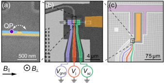
Our device is a single-island OCS transmon dispersively coupled to a half-wave resonator, used to read out the state of the qubit Koch et al. (2007) 111We measure the exact same device as Bargerbos et al. (2020). The transmon is based on a superconducting-semiconducting (SC-SM) Al/InAs NW JJ [\Freffig:device(a)] Krogstrup et al. (2015). The JJ divides the NW in two Al-proximitized InAs sections. One section is connected to a NbTiN ground plane and the other to a NbTiN island, with charging energy [\Freffig:device(b)]. The island is capacitively coupled to a superconducting coplanar waveguide resonator for readout with and with a coupling strength of [\Freffig:device(c)]. The resonator, ground plane and island are patterned with vortex pinning sites Kroll et al. (2019). The carrier density in the semiconducting JJ and adjacent leads are tuned by several electrostatic gates through the field effect [\Freffig:device(d)]. First, we alter the Josephson coupling by Doh et al. (2005), similarly to previous work in the context of SM weak link qubits Larsen et al. (2015); de Lange et al. (2015); Luthi et al. (2018). In addition, the carrier density profile in the SC-SM parts of the leads are tuned by the wrapped plunger gates and , enabling us to control the proximity effect in the enclosed leads Antipov et al. (2018); de Moor et al. (2018); Winkler et al. (2019). Lastly, the offset charge of the island is predominantly tuned by . We note that tuning requires much smaller ranges in voltage (on the order of ) than the voltages required to tune the carrier density appreciably (typically requiring ), providing an effectively independent tuning knob for .
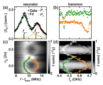
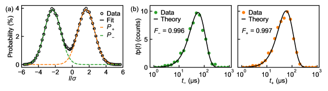
We first demonstrate readout of the charge-parity of the OCS transmon via the superconducting microwave resonator response in absence of an additional qubit drive tone Serniak et al. (2019). The -ratio is designed to be when the qubit’s ground to first excited state transition frequency , making the qubit transitions depend strongly on parity and [\Freffig:resonator_response(b,d)] Koch et al. (2007). As a consequence of the strong dispersive coupling between the OCS transmon and resonator, the resonator frequency inherits these same dependencies on and [\Freffig:resonator_response]. We verify this by investigating the correspondence between the -dependent resonator frequencies, and 222The different magnitudes of for and are only found with the TWPA activated., and the two qubit parity branches, and , respectively. By matching the probe frequency () to () we demonstrate selective sensitivity to () in two-tone spectroscopy at maximum charge-parity separation () [\Freffig:resonator_response (a,b)]. The even and odd charge-parity branches are observed simultaneously, consistent with the transfer of one or more QPs across the JJ during each measurement. Our cQED setup allows us to detect individual parity switching events in real time. The QPP dynamics, and its dependence on electric and magnetic field, is central to this work.
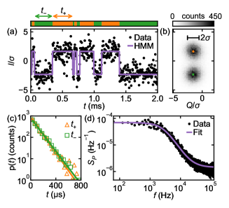
We demonstrate our ability to measure QPP in real time. By monitoring at a fixed readout frequency, we can directly detect island-parity switching events down to resolution by utilizing a near-quantum limited travelling-wave parametric amplifier Macklin et al. (2015). To maximize signal to noise, the readout is performed at with set at the local minimum in between the two parity resonances. Recording a continuous measurement of reveals a random telegraph signal [\Freffig:QPP_Analysis(a)] as a consequence of the switches in qubit-island parity. The histogram of in the complex ()-plane confirms two well-separated parity states [\Freffig:QPP_Analysis(b)], both Gaussian distributed with symmetric widths and populations SI . The histogram is built by constructing a connected time series of ()-shots of by binning -long time traces in bins. The equal parity population, as expected with the ground state charge dispersion being two orders smaller than the thermal energy, makes the two parity levels indistinguishable and hinders ‘even’ and ‘odd’ state labelling. Instead, we refer to ‘+’ and ‘-’ as unspecified parity labels.
To gain further insight in the poisoning dynamics, we assign a state to every ()-shot by applying a hidden Markov model (HMM) to the time evolution of [\Freffig:QPP_Analysis(a)].
The extracted dwell times and are found to follow an exponential probability distribution with average dwell times of and [\Freffig:QPP_Analysis(c)].
The exponential distribution indicates that the switching events result from a Poissonian process.
The Poissonian temporal distribution together with the Gaussian distributed parity clusters validate the use of the HMM SI .
The overlap of the dwell time distributions, both in number of counts and average dwell times, demonstrates the symmetry between the even-to-odd and odd-to-even poisoning processes.
This justifies the extraction of a single parity lifetime via Fourier transform analysis [\Freffig:QPP_Analysis(d)]; each long jump trace is transformed to frequency space separately and subsequently averaged, revealing a power spectral density (PSD) that is well fitted by a Lorentzian SI .
The typical drop off frequency corresponds to the combined average parity lifetime , where and a parity detection fidelity of in the case of , where the uncertainties are extracted errors from the fit.
We now use the measurement of QPP dynamics to investigate the response of the device to static electromagnetic field tuning. For these measurements ten individual measurements of are averaged over minute timescales to constitute . The associated standard deviation in captures any excess variation in stemming from temporal fluctuations in the QP density Grünhaupt et al. (2018); Vool et al. (2014). First, we confirm that the observed QP dynamics result from the presence of non-equilibrium QPs, by measuring the temperature dependence of SI . At the lowest temperature of the extracted QP to Cooper pair ratio is , which corresponds to a thermal QP distribution with an effective temperature of . These numbers are typically encountered Ristè et al. (2013); Aumentado et al. (2004); Vool et al. (2014); Wang et al. (2014); Taupin et al. (2016), and are linked to stray radiation impacting the device due to imperfect shielding Serniak et al. (2019); Houzet et al. (2019); Vepsäläinen et al. (2020).
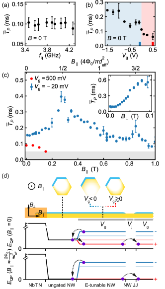
We take advantage of the semiconducting nature of the NW to electrostatically modify the charge-carrier density in the JJ and its leads de Moor et al. (2018); Antipov et al. (2018); Winkler et al. (2019). First we verify that does not strongly influence the QP tunneling rate by varying through [\Freffig:Tp_dependencies(a)]. We measure a constant while changing over almost , corresponding to a increase in . This justifies any retuning of amidst a measurement series, a necessary intervention to ensure that stays within a frequency range suitable for parity lifetime readout over large field ranges. We then investigate the gate dependence of by varying both plunger gate voltages simultaneously [\Freffig:Tp_dependencies(b)]. For we observe a decrease in , while for we find to rise quickly initially and more than doubles upon further decreasing .
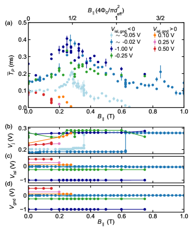
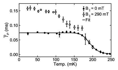
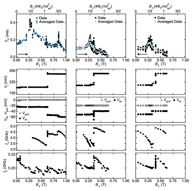
The connection between at the JJ and the proximity effect in the leads can be further explored by applying a magnetic field [\Freffig:Tp_dependencies(c)]. For this we are able to operate the device as a charge parity detector up to , where is oriented along the NW. For we observe a decay of with SI , indicating increased near the JJ as associated with the closing with magnetic field of the proximity-induced gap in the gated parts of the leads. At , we observe a markedly different dependence of . Upon increasing , further rises and exhibits clear peaks at distinct values of . The transition point at that divides these two regimes suggests that the device behaviour hinges on the energy potential landscape for QPs set by the profile of the proximity-induced gap in the gated and ungated NW sections.
In the case of , -enhancements indicate the turn-on of magnetic field induced QP trapping away from the JJ. We observe enhancements of for distinct values for . We attribute these to the orbital effect of the magnetic field, that occurs when the cylindrical electron density in the leads is threaded by magnetic flux, leading to the suppression of the proximity-induced gap [\Freffig:Tp_dependencies(d)] Büttiker and Klapwijk (1986); Kringhøj et al. (2021); Stampfer et al. (2021). Such a cylindrical electron density profile is a manifestation of charge accumulation at the InAs NW surface for Winkler et al. (2019). However, in the NW sections leading up to the JJ we can locally interrupt the accumulation by applying , preventing such gap suppression. The larger-gap sections obstruct QPs trapped in the ungated regions from reaching the JJ and thus acts as QP filters Ménard et al. (2019). The situation reverses upon setting , which activates the gap suppression and QP trapping right next to the JJ, decreasing as increases. From the peak positions we estimate an effective diameter of of the ungated NW sections, suggesting an accumulation layer of about based on the measured NW diameter of and consistent with simulations Antipov et al. (2018). Lastly, we apply an out of plane field [\Freffig:Tp_dependencies(c) inset]. We now observe an even more dramatic dramatic increase of at much more moderate fields, starting from . For perpendicular field orientation we do not expect the orbital effect to play a considerable role. Instead, we deem it more likely that the observed increase is caused by QP trapping in vortex cores induced in the NbTiN contacts Wang et al. (2014); Taupin et al. (2016), whose presence is also evidenced by the broadening of the resonator lineshape Kroll et al. (2019). The resonator broadening prevented exploring higher ranges for .
In conclusion, we have realized an OCS Al/InAs NW transmon that operates up to magnetic fields of , establishing a real-time charge-parity switching detector at strong magnetic fields. We demonstrated a more than twofold increase in charge-parity lifetime by applying a local electrostatic potential and a global magnetic field, thereby controlling the minimal QP excitation energy in the leads of the JJ. At negative gate voltages a QP filter forms at the JJ, trapping QPs away from the JJ. The orbital effect suppresses the proximity-induced gap at half integer magnetic flux threading of the nanowire, increasing the efficiency of the QP traps and yielding magnetic field dependent parity lifetime enhancements. At positive voltages and finite fields QPs are trapped at the JJ, resulting in significant drop in parity lifetime. The demonstrated increase in parity lifetime via electric and magnetic field induced in-situ gap engineering, provides a realistic solution to QPP by non-equilibrium QPs, important for quantum computation with both topological and superconducting qubits.
Acknowledgements
We thank K. Peterson, A. Kringhøj, L. Casparis, T. Larsen, B. van Heck, D. Pikulin, T. Karzig, F. Rybakov, E. Babaev, K. Serniak, and B. Nijholt for the open and stimulating discussions, J. van Veen for depositing the NW and W. D. Oliver lab for providing a traveling wave parametric amplifier.
This work was supported by the Netherlands Organisation for Scientific Research (NWO/OCW) as part of the Frontiers of Nanoscience (NanoFront) program, Microsoft Corporation Station Q and the European Research Council.
References
- Day et al. (2003) P. K. Day, H. G. LeDuc, B. A. Mazin, A. Vayonakis, and J. Zmuidzinas, Nature 425, 817 (2003).
- Pekola et al. (2008) J. P. Pekola, J. J. Vartiainen, M. Möttönen, O.-P. Saira, M. Meschke, and D. V. Averin, Nature Physics 4, 120 (2008).
- Giazotto et al. (2006) F. Giazotto, T. T. Heikkilä, A. Luukanen, A. M. Savin, and J. P. Pekola, Rev. Mod. Phys. 78, 217 (2006).
- Aumentado et al. (2004) J. Aumentado, M. W. Keller, J. M. Martinis, and M. H. Devoret, Phys. Rev. Lett. 92, 066802 (2004).
- de Visser et al. (2011) P. J. de Visser, J. J. A. Baselmans, P. Diener, S. J. C. Yates, A. Endo, and T. M. Klapwijk, Phys. Rev. Lett. 106, 167004 (2011).
- van Woerkom et al. (2015) D. J. van Woerkom, A. Geresdi, and L. P. Kouwenhoven, Nature Physics 11, 547 EP (2015).
- Sun et al. (2012) L. Sun, L. DiCarlo, M. D. Reed, G. Catelani, L. S. Bishop, D. I. Schuster, B. R. Johnson, G. A. Yang, L. Frunzio, L. Glazman, M. H. Devoret, and R. J. Schoelkopf, Phys. Rev. Lett. 108, 230509 (2012).
- Ristè et al. (2013) D. Ristè, C. C. Bultink, M. J. Tiggelman, R. N. Schouten, K. W. Lehnert, and L. DiCarlo, Nature Communications 4, 1913 (2013).
- Wang et al. (2014) C. Wang, Y. Y. Gao, I. M. Pop, U. Vool, C. Axline, T. Brecht, R. W. Heeres, L. Frunzio, M. H. Devoret, G. Catelani, L. I. Glazman, and R. J. Schoelkopf, Nature Communications 5, 5836 (2014).
- Janvier et al. (2015) C. Janvier, L. Tosi, L. Bretheau, Ç. Ö. Girit, M. Stern, P. Bertet, P. Joyez, D. Vion, D. Esteve, M. F. Goffman, H. Pothier, and C. Urbina, Science 349, 1199 (2015).
- Riwar et al. (2016) R.-P. Riwar, A. Hosseinkhani, L. D. Burkhart, Y. Y. Gao, R. J. Schoelkopf, L. I. Glazman, and G. Catelani, Phys. Rev. B 94, 104516 (2016).
- Hays et al. (2018) M. Hays, G. de Lange, K. Serniak, D. J. van Woerkom, D. Bouman, P. Krogstrup, J. Nygård, A. Geresdi, and M. H. Devoret, Phys. Rev. Lett. 121, 047001 (2018).
- Serniak et al. (2019) K. Serniak, S. Diamond, M. Hays, V. Fatemi, S. Shankar, L. Frunzio, R. Schoelkopf, and M. Devoret, Phys. Rev. Applied 12, 014052 (2019).
- Karzig et al. (2021) T. Karzig, W. S. Cole, and D. I. Pikulin, Phys. Rev. Lett. 126, 057702 (2021).
- Kaplan et al. (1976) S. B. Kaplan, C. C. Chi, D. N. Langenberg, J. J. Chang, S. Jafarey, and D. J. Scalapino, Phys. Rev. B 14, 4854 (1976).
- Taupin et al. (2016) M. Taupin, I. M. Khaymovich, M. Meschke, A. S. Mel’nikov, and J. P. Pekola, Nature Communications 7, 10977 (2016).
- Ménard et al. (2019) G. C. Ménard, F. K. Malinowski, D. Puglia, D. I. Pikulin, T. Karzig, B. Bauer, P. Krogstrup, and C. M. Marcus, Phys. Rev. B 100, 165307 (2019).
- de Moor et al. (2018) M. W. A. de Moor, J. D. S. Bommer, D. Xu, G. W. Winkler, A. E. Antipov, A. Bargerbos, G. Wang, N. van Loo, R. L. M. O. het Veld, S. Gazibegovic, D. Car, J. A. Logan, M. Pendharkar, J. S. Lee, E. P. A. M. Bakkers, C. J. Palmstrøm, R. M. Lutchyn, L. P. Kouwenhoven, and H. Zhang, New Journal of Physics 20, 103049 (2018).
- Lutchyn et al. (2018) R. M. Lutchyn, E. P. A. M. Bakkers, L. P. Kouwenhoven, P. Krogstrup, C. M. Marcus, and Y. Oreg, Nature Reviews Materials 3, 52 (2018).
- van Veen et al. (2018) J. van Veen, A. Proutski, T. Karzig, D. I. Pikulin, R. M. Lutchyn, J. Nygård, P. Krogstrup, A. Geresdi, L. P. Kouwenhoven, and J. D. Watson, Phys. Rev. B 98, 174502 (2018).
- Kroll et al. (2019) J. G. Kroll, F. Borsoi, K. L. van der Enden, W. Uilhoorn, D. de Jong, M. Quintero-Pérez, D. J. van Woerkom, A. Bruno, S. R. Plissard, D. Car, E. P. A. M. Bakkers, M. C. Cassidy, and L. P. Kouwenhoven, Phys. Rev. Applied 11, 064053 (2019).
- de Lange et al. (2015) G. de Lange, B. van Heck, A. Bruno, D. J. van Woerkom, A. Geresdi, S. R. Plissard, E. P. A. M. Bakkers, A. R. Akhmerov, and L. DiCarlo, Phys. Rev. Lett. 115, 127002 (2015).
- Larsen et al. (2015) T. W. Larsen, K. D. Petersson, F. Kuemmeth, T. S. Jespersen, P. Krogstrup, J. Nygård, and C. M. Marcus, Phys. Rev. Lett. 115, 127001 (2015).
- Luthi et al. (2018) F. Luthi, T. Stavenga, O. W. Enzing, A. Bruno, C. Dickel, N. K. Langford, M. A. Rol, T. S. Jespersen, J. Nygård, P. Krogstrup, and L. DiCarlo, Phys. Rev. Lett. 120, 100502 (2018).
- Pita-Vidal et al. (2020) M. Pita-Vidal, A. Bargerbos, C.-K. Yang, D. J. van Woerkom, W. Pfaff, N. Haider, P. Krogstrup, L. P. Kouwenhoven, G. de Lange, and A. Kou, Phys. Rev. Applied 14, 064038 (2020).
- Kringhøj et al. (2021) A. Kringhøj, T. W. Larsen, O. Erlandsson, W. Uilhoorn, J. Kroll, M. Hesselberg, R. McNeil, P. Krogstrup, L. Casparis, C. Marcus, and K. Petersson, Phys. Rev. Applied 15, 054001 (2021).
- Büttiker and Klapwijk (1986) M. Büttiker and T. M. Klapwijk, Phys. Rev. B 33, 5114 (1986).
- Zuo et al. (2017) K. Zuo, V. Mourik, D. B. Szombati, B. Nijholt, D. J. van Woerkom, A. Geresdi, J. Chen, V. P. Ostroukh, A. R. Akhmerov, S. R. Plissard, D. Car, E. P. A. M. Bakkers, D. I. Pikulin, L. P. Kouwenhoven, and S. M. Frolov, Phys. Rev. Lett. 119, 187704 (2017).
- Winkler et al. (2019) G. W. Winkler, A. E. Antipov, B. van Heck, A. A. Soluyanov, L. I. Glazman, M. Wimmer, and R. M. Lutchyn, Phys. Rev. B 99, 245408 (2019).
- Stampfer et al. (2021) L. Stampfer, D. J. Carrad, D. Olsteins, C. E. N. Petersen, S. A. Khan, P. Krogstrup, and T. S. Jespersen, “Andreev interference in the surface accumulation layer of half-shell inassb/al hybrid nanowires,” (2021), arXiv:2104.00723.
- Pekker et al. (2013) D. Pekker, C.-Y. Hou, V. E. Manucharyan, and E. Demler, Phys. Rev. Lett. 111, 107007 (2013).
- Ginossar and Grosfeld (2014) E. Ginossar and E. Grosfeld, Nature Communications 5, 4772 (2014).
- Koch et al. (2007) J. Koch, T. M. Yu, J. Gambetta, A. A. Houck, D. I. Schuster, J. Majer, A. Blais, M. H. Devoret, S. M. Girvin, and R. J. Schoelkopf, Phys. Rev. A 76, 042319 (2007).
- Note (1) We measure the exact same device as Bargerbos et al. (2020).
- Krogstrup et al. (2015) P. Krogstrup, N. Ziino, W. Chang, S. Albrecht, M. Madsen, E. Johnson, J. Nygård, C. Marcus, and T. Jespersen, Nature Materials 14, 400 (2015).
- Doh et al. (2005) Y.-J. Doh, J. A. van Dam, A. L. Roest, E. P. A. M. Bakkers, L. P. Kouwenhoven, and S. De Franceschi, Science 309, 272 (2005).
- Antipov et al. (2018) A. E. Antipov, A. Bargerbos, G. W. Winkler, B. Bauer, E. Rossi, and R. M. Lutchyn, Phys. Rev. X 8, 031041 (2018).
- Note (2) The different magnitudes of for and are only found with the TWPA activated.
- Macklin et al. (2015) C. Macklin, K. O’Brien, D. Hover, M. E. Schwartz, V. Bolkhovsky, X. Zhang, W. D. Oliver, and I. Siddiqi, Science 350, 307 (2015).
- (40) See the Supplemental Material for detailed information on the device fabrication, set-up, magnetic field characterisation, validation of the HMM, fitting model for the PSD, temperature measurements and additional magnetic field data on the parity lifetime trends.
- Grünhaupt et al. (2018) L. Grünhaupt, N. Maleeva, S. T. Skacel, M. Calvo, F. Levy-Bertrand, A. V. Ustinov, H. Rotzinger, A. Monfardini, G. Catelani, and I. M. Pop, Phys. Rev. Lett. 121, 117001 (2018).
- Vool et al. (2014) U. Vool, I. M. Pop, K. Sliwa, B. Abdo, C. Wang, T. Brecht, Y. Y. Gao, S. Shankar, M. Hatridge, G. Catelani, M. Mirrahimi, L. Frunzio, R. J. Schoelkopf, L. I. Glazman, and M. H. Devoret, Phys. Rev. Lett. 113, 247001 (2014).
- Houzet et al. (2019) M. Houzet, K. Serniak, G. Catelani, M. H. Devoret, and L. I. Glazman, Phys. Rev. Lett. 123, 107704 (2019).
- Vepsäläinen et al. (2020) A. P. Vepsäläinen, A. H. Karamlou, J. L. Orrell, A. S. Dogra, B. Loer, F. Vasconcelos, D. K. Kim, A. J. Melville, B. M. Niedzielski, J. L. Yoder, S. Gustavsson, J. A. Formaggio, B. A. VanDevender, and W. D. Oliver, Nature 584, 551 (2020).
- Bargerbos et al. (2020) A. Bargerbos, W. Uilhoorn, C. Yang, P. Krogstrup, L. P. Kouwenhoven, G. de Lange, B. van Heck, and A. Kou, Phys. Rev. Lett. 124, 246802 (2020).
Supplemental materials for “Field induced quasiparticle trapping in a hybrid superconducting-semiconducting circuit”
Supplemental materials for “Quasiparticle trapping by orbital effect in a hybrid superconducting-semiconducting circuit”
I Device overview and experimental setup
As a substrate we use high resistivity silicon coated with of low pressure chemical vapor deposition silicon nitride (SiNx) to prevent gate leakage at small gate separation. A thin layer of NbTiN is sputtered onto the 3” wafer from a pure target in an \chAr/N_2 atmosphere. We chose \chNbTiN for its high upper critical field () and compatibility with microwave frequency circuits. The coplanar waveguide (CPW) resonator, capacitor island, ground plane, bottom gate and LC-filters for the dc gate lines are all shaped from the base layer by reactive ion etching in a SF6/O2 plasma. The on-chip LC-filters are low pass filters that decouple the device from the off-chip circuitry at microwave frequencies. In this same etching step the entire chip is patterned with artificial pinning sites to trap Abrikosov vortices Kroll et al. (2019). The microwave resonator is asymmetrically coupled to its in- and output, where a lower coupling at the input prevents unnecessary losses. To electrostatically isolate the bottom gate, of SiNx is deposited by plasma-enhanced chemical vapor deposition and shaped by wet etching with buffered oxide etch (20:1). An indium arsenide (InAs) nanowire with epitaxial two-faceted thin-film aluminum (Al) shell Krogstrup et al. (2015) is aligned with respect to the bottom gate using a micromanipulator setup. The long Josephson junction (JJ) is defined by a selective transene-D wet etch stripping the Al shell in the middle of the wire. Simultaneously a long part of the Al shell is also removed at the ends of the wire in preparation for the metallic contact patches. of \chNbTiN is sputtered to contact both ends to the \chNbTiN base, one end to ground and the other to the capacitor island. The \chNbTiN patches overlap slightly with the remaining Al shell. Local electrostatic tuning of the electron density in the wire is made possible by sputtering of SiNx followed by of sputtered NbTiN to form so-called wrap gates.
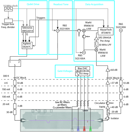
The chip is cooled down in a dilution refrigerator with base temperature of and equipped with 3-axis vector magnet. To make place for the vector magnet the coldest radiative shield is mounted at and is not even light-tight. To compensate for the lesser shielding the sample is placed in a copper casing encapsulated by several layers of eccosorb material and copper tape to absorb and reflect radiation. Standard heterodyne measurement techniques are used to readout out the magnitude and phase response of the sample [\Freffig:setup]. To reduce the large parameter space the bottom gate was kept at throughout these experiments.
II Transmon characterisation in Magnetic Field
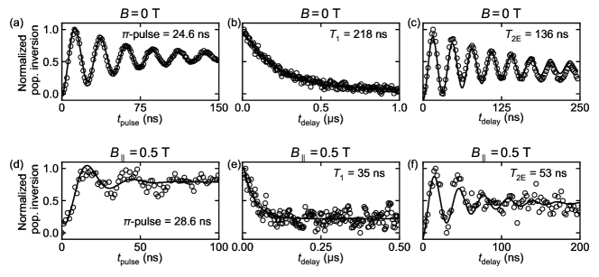
To characterize the performance of the transmon we measure the energy relaxation and phase coherence times both at and [\Freffig:Suppl_TD], demonstrating coherent control of the the transmon at large magnetic fields. The measurements at correspond to a transmon frequency of with readout tone set to at gate settings , and . The parameter space where the transmon is measurably close to the resonator is significantly reduced at . Therefore measurements were taken at different settings; , and , resulting in and . Both and times are significantly shorter than the observed parity lifetimes, showing that the coherence of our device is not limited by quasiparticle induced losses. Possible dominating decoherence mechanisms may be the lack of radiative shielding, unfiltered microwave lines and dielectric material losses.
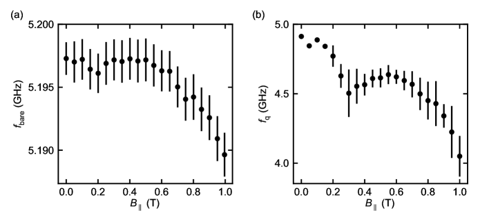
To further demonstrate the magnetic field compatibility we track the bare resonator response [\Freffig:Suppl_fq_vs_Ba] and the qubit frequency with [\Freffig:Suppl_fq_vs_Bb]. To ensure similar gate settings for the whole -range, the measurement sequence was performed starting from at , and . Magnetic field alignment was performed at every magnetic field measurement to ensure the optimal alignment. The bare resonator response, measured at high input power, shows a decreasing trend only from on, leading us to believe this is the threshold for pinning all vortices in the resonator for our design. The slight dip in around is attributed to the dissipative loading of environmental paramagnetic electron spin resonances with Landé -factor of Kroll et al. (2019). Two-tone spectroscopy of the simultaneously tracked qubit frequency reveals a non-monotonic decay. The general decreasing trend is consistent with a decreasing supercurrent due the closing of the superconducting gap. Comparison to [\Freffig:overview_Bparallel] shows that depends more strongly on at more positive voltages. This observation is in agreement with the density of states being confined towards the superconducting shell, improving the induced superconducting gap. We observe a local minimum around , consistent with the flux induced interference effects as explained in the main text, and also reported by Kringhøj et al. (2021); Stampfer et al. (2021).
III Validation of hidden Markov model
As discussed in the main text, the assignment of a charge parity state to a data point is done by the use of a hidden Markov model (HMM) Vool et al. (2014). To validate the use of a HMM to our data set, we show the two levels are normally distributed in the () space [\Freffig:Suppl_HMM(a)] and that the quantum jumps follow a Poisson distribution in time. Deviation from a Gaussian distribution can indicate too long averaging per data point, not only averaging out noise but also averaging out the sharp jumps. Secondly, the HMM is only applicable to Markovian processes that follow a Poissonian distribution in dwell time. The exponential distribution shown in the main text verifies Poissonian behavior of the switching process. For a complete check, we verify the Poissonian behaviour also for the weighted histogram [\Freffig:Suppl_HMM(b)]. Here the visibility of the low-frequency switches is increased. Comparison to the theory allows us to compute the fidelity:
| (1) |
where are the measured values and the predicted values. We find fidelities of and .
IV Parity lifetime extraction from PSD
By use of the HMM we have shown symmetric transition dynamics, i.e. equal lifetimes and fidelities for the charge parity states. This allows us to extract a combined charge parity lifetime with a combined detection fidelity by fitting the averaged power spectral density (PSD). determines the detection error probability , an uncorrelated noise process masking the random telegraph signal (RTS). The transformation to the frequency domain is computationally beneficial, besides the SNR of the PSD can be increased while preserving high frequency information by averaging Fourier transforms of consecutive non-integrated time traces. The PSD of a RTS is described by a Lorentzian Ristè et al. (2013):
| (2) |
where is the average parity jump rate, the detection fidelity and the integration time.
V Effective quasiparticle temperature
To investigate whether the main source of QPs are of non-thermal origin we measure the temperature dependence of , both at (at , , ) and at (at , , ) [\Freffig:Temp]. is determined from the Lorentzian fit of the frequency spectrum and we average 10 measurements to provide a standard deviation. We assume that the QPP rate is proportional to the QP density . is taken as the QP density normalized by the density of Cooper pairs in thermal equilibrium and consists of two independent contributions:
| (3) |
Here the first term covers the temperature independent contribution and the second term describes the temperature dependent contribution determined by scattering and recombination processes of QPs localized near the gap edge Kaplan et al. (1976). The data is well-fitted by the model with , equivalent to an effective temperature of , and . Our result is similar to previously recorded QP ratios of to Aumentado et al. (2004); Vool et al. (2014); Wang et al. (2014); Taupin et al. (2016). Furthermore, is consistent with DC measurements for thin aluminium films of , indicating a near-perfect proximitized superconducting gap. To gain further insight at finite magnetic field we repeated the measurement at [\Freffig:Temp]. A similar drop off around shows the device is still plagued by the same source of non-equilibrium QPs. However, the cascading drop off can not be described by the theoretical model and therefore leads us to believe that the mechanism for -enhancement depends on temperature as well with a characteristic temperature that lies below .
VI Parity lifetime versus magnetic field
To demonstrate that the parity lifetime enhancement is a reproducible feature and is independent of the sweep direction, we repeated the measurement using different gate settings and sweep directions [\Freffig:overview_Bparallel]. For completeness, all gate settings, readout frequency and available qubit frequency data are plotted along side. The decreasing with shows the necessity of retuning some parameters during a measurement run, since the readout of is only possible in the range where . We show here both the raw data and the averaged data, where averaging only has been applied to identical gate settings. We observe an enhancement in for all three runs with the maximum at .
Additional plunger settings are investigated to verify the difference between positive and negative [\Freffig:test]. The magnetic field alignment at each increment is time consuming. To save time, measurements of are taken by first sweeping over different gate settings before increasing . The measurement order results in a more capricious data set since the sweeping of gate voltages is prone to hysteresis. Around , we observe an enhancement of for all , while we observe an impairment of for . The magnetic field value where the enhancement of is observed seems identical. Contrarily, the value at which dips is observed to depend on the magnitude of the positive voltage applied to the plunger gates. These observations suggest that the origin of the -enhancement is not located at the gated NW sections, while the phenomenon behind the -dips does occur at the gated NW sections.