Josephson Junctions Via Anodization of Epitaxial Al on an InAs Heterostructure
Abstract
We combine electron beam lithography and masked anodization of epitaxial aluminium to define tunnel junctions via selective oxidation, alleviating the need for wet-etch processing or direct deposition of dielectric materials. Applying this technique to define Josephson junctions in proximity-induced superconducting Al-InAs heterostructures, we observe multiple Andreev reflections in transport experiments, indicative of a high quality junction. We further compare the mobility and density of Hall-bars defined via wet etching and anodization. These results may find utility in uncovering new fabrication approaches to junction-based qubit platforms.
Zero energy modes in a 1-dimensional (1D) topological superconductor are candidate building blocks for high-fidelity quantum computation Kitaev (2001); Nayak et al. (2008). One proposed approach to realising a topological superconductor is via a 2-dimensional electron gas (2DEG) with large spin-orbit interaction, proximity coupled to a conventional superconductor and confined to 1D using electrostatic gates and tunnel barriers Lutchyn et al. (2010); Oreg et al. (2010); Mourik et al. (2012). Such a configuration is experimentally challenging to realize however, since many of the needed parameters also compete with each other. Inducing superconductivity Kjaergaard et al. (2016), for instance, requires that the 2DEG be close to the superconductor, where disorder from surface states can also greatly degrade the mobility Hatke et al. (2017).
Josephson junctions or tunnel barriers separating topological segments from normal regions are particularly sensitive to disorder. Typically, crystaline superconductors, grown using molecular beam epitaxy (MBE) are etched away using invasive wet chemical processing or damaging dry etchant techniques Richter et al. (2002); Heida et al. (1998); Mur et al. (1996). This approach is often used to create, for example, the weak link of a Josephson junction via wet etching of Al (usually with transene) Fornieri et al. (2019). Although there is opportunity to further optimize the etching process Pauka et al. (2020), circumventing the need for it entirely would likely lead to junctions with less disorder. An associated challenge is the patterning of features on the length-scale of a few tens of nanometers in device structures, for example, to be able to reach the Josephson short-junction limit Peng et al. (2016). At these length-scales wet-etching can be difficult to control.
Here, we report the use of anodization to define a Josephson junction via the selective oxidation of epitaxial aluminium on an InAs heterostructure. In addition to being largely non-invasive, the technique offers a means of defining structures with a resolution limited, in-principle, only by the nanometer precision of the electron beam lithography. In a straight up comparison we also show that Hall bars defined via anodization have a moderately higher mobility than devices that are shaped by wet-etch processing.
Anodization is a standard industrial method used extensively to protect or modify the properties of surfaces Diggle et al. (1969). It has a wide range of applications, most abundantly for protecting metallic objects from uncontrolled oxidation. In the field of device physics, it has been used to define Nb Josephson junctions Kroger et al. (1981).
The anodization circuit is realized such that the target metal constitutes the anode. By driving a current through the target metal submerged in a suitable electrolyte, an oxydo-reduction reaction can be induced. In the case of Al, alumina () is formed:
| (1) |
This process allows for the controlled oxidation of Al to proceed to a specific depth beyond the 3 nm native oxide Mott (1947), at a rate fixed by the applied current Hunter and Fowle (1954).
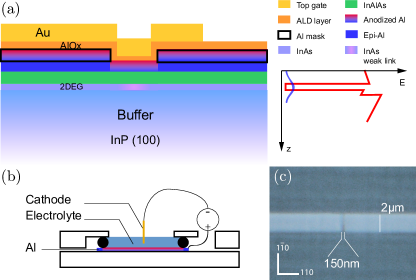
Turning to quantum devices, we make use of this reaction to define tunnel barriers in materials comprising superconducting heterostructures. Unlike conventional fabrication approaches that remove the Al superconductor and back-fill with dielectric, here we rather use a second lift-off patterned layer of evaporated Al (Al-mask) on top of the epi-Al and employ the anodization process. In this way, we are able to retain the high-resolution pattern of the evaporated Al-mask, and, also the high-quality interface between the heterostructure and the newly formed dielectric near the shallow quantum well.
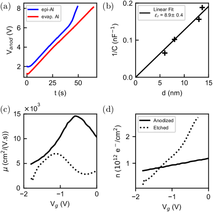
Starting from an InAlAs/InAs/InGaAs heterostructure (quantum well 10 nm below the surface and 7 nm of in situ grown epi-Al), Hatke et al. (2017), a poly(methyl methacrylate) resist is spin-coated and patterned using electron beam lithography, as shown in Fig. 1 (a). The Al-mask layer – the same thickness as the epi-Al layer – is then evaporated and the pattern formed using the lift-off technique. Immediately prior to the evaporation of the Al-mask layer, in the same vaccum cycle, an Ar ion mill step is performed to remove the native oxide from the epi-Al, ensuring good electrical contact between the two Al layers. The sample is then placed in a setup as shown in Fig. 1 (b), submerged in an electrolyte – a mixture of ammonium pentaborate tetra-hydrate and ethylene glycol Kroger et al. (1981) – and connected to the positive terminal of the current source. Thereby the surface Al constitutes the anode. A needle is used as the cathode, and is placed into the electrolyte solution a small distance from the sample. The structure is anodized using a current of 50 A and up to 6 V [Fig. 1 (c)]. While a fixed current is passing through the anodization circuit, a voltage , exists across the developing oxide (thickness, ). This voltage is fixed by the critical electric field, , needed to force the ions through the oxide layer Diggle et al. (1969). This voltage increases linearly with time during anodization and allows us to monitor the thickness of the oxide layer and the rate of anodization, as shown in Fig. 2 (a). By monitoring as a function of time, the effective depth of the anodized Al can be determined.
The anodization is stopped at a known voltage, , which corresponds to the thickness of the Al-mask. In this way, the Al-mask has effectively been anodized instead of the epi-Al in the specifically patterned regions. The regions that were not covered by the Al-mask are now fully insulating, while the parts of the epi-Al which where covered with the Al-mask are now covered with a layer of alumina. An anodization rate of 100 mV/s for both the Al-mask and epi-Al has been measured. It is worth emphasizing that for this method to work the rates for both must be equal. This ensures that the Al-mask and the uncovered epi-Al layer will be fully anodized at the same point in time.
Following the anodization, a mesa structure is etched in order to avoid top-gate leakage. The alumina around the mesa is removed using a developing solution, AZ726, followed by a dilute phosphoric acid etch. Finally, a 5 nm thick alumina layer is grown by ALD and the Ti/Au top-gates are deposited, as shown in Fig. 1 (a).
The anodization ratio of oxide thickness, , to measured voltage, , was determined by performing ellipsometry on test samples anodized to different depths. A ratio of 1.37 was found, which is consistent with values in the literature Diggle et al. (1969); Hunter and Fowle (1954). A further corroboration of the extrapolated rate is the clear kink in vs. of the epi-Al anodization, which can be seen in Fig. 2 (a). This voltage translates to an epi-Al thickness of 7 nm, which matches that measured by X-ray diffraction. The change of rate of anodization corresponds to a higher critical electric field, , needed to force ions through the InAlAs layer. Consistent with this picture we estimate the dielectric constant of the oxide by measuring the capacitance, , between two patterned pads of surface, , with different anodized alumina of known thickness, , see Fig. 2 (b). The relative permeability was found to be, .
Next, we compare the mobility and electron density of Hall bars defined using standard wet etching to those defined by anodization, as shown in Fig. 2 (c) and Fig. 2 (d). Here, data is taken at an electron temperature of mK. For the Hall-bar defined using anodization, the mobility at () was found to be cm2/(V.s), with electron density () e-/cm2, comparable to values given in the literature Tschirky et al. . Application of a negative gate voltage leads to a peak mobility of cm2/(V.s) The variation in mobility as a function of applied top-gate voltage is consistent with screening of charge impurities by electrons in the 2DEG Umansky et al. (1997).
For comparison, a sample from the same wafer was patterned into a Hall bar using an optimised standard Transene type-D etch Pauka et al. (2020) (otherwise processed identically) and was found to have a peak mobility of cm2/(V.s). We underscore the improvement in mobility of the device fabricated using anodization, indicating the sensitivity of these device structures to disorder induced by chemical processing. Also of note, for the anodized Hall bar, the electron density at is around half that of the chemically etched device. A similar anodization method has also recently yielded an enhancement of the mobility Drachmann et al. (2021).
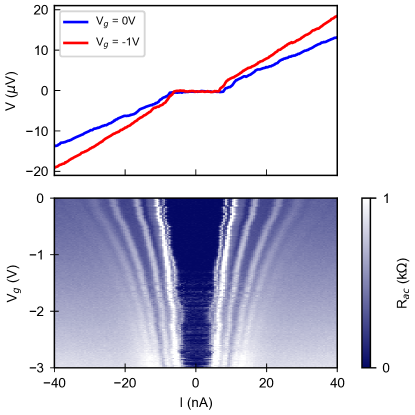
Finally, to demonstrate the utility of this technique for nanoscale device fabrication, a Josephson junction with a barrier region of length 150 nm was fabricated using anodization, as shown in Fig. 1 (c). The device was characterized using a standard dc transport making use of a current-bias with four-point measurement in a dilution refrigerator with an electron temperature of mK – (determined using an NIS junction Feshchenko et al. (2015)). The epi-Al layer has a critical temperature above K and an in-plane critical magnetic field, T Suominen et al. (2017). The mobility obtained from the Hall measurements corresponds to an elastic scattering length, nm, which suggests the junction is in the quasi-ballistic limit.
The current–voltage characteristics of the device as a function of applied top-gate voltage can be seen in Fig. 3. Despite the relatively low critical current compared to similar devices in the literature Mayer et al. (2019), multiple Andreev reflections (MAR) are clearly resolved which indicates that the electrons remain phase coherent over multiple times the length of the weak link.
With increasing negative applied top-gate voltage, the 2DEG is depleted and the critical current decreases, as shown in the lower panel of Fig. 3. Below V, the junction loses phase coherence and a finite voltage appears across the weak link. The characteristic voltage or product is constant between 0 V and -1.5 V (see SI) at around 3 eV, which is a few percent of the Al gap, V. As an indication, the excess current at -1 V is measurable and is nA, which is approximately 15% of the critical current. Although lower than the value expected for a fully transparent interface Kjærgaard et al. (2017); Blonder et al. , further investigations into the exact nature of the induced superconducting gap, , in this particular type of heterostructure need to be performed in order to fully understand this discrepancy.
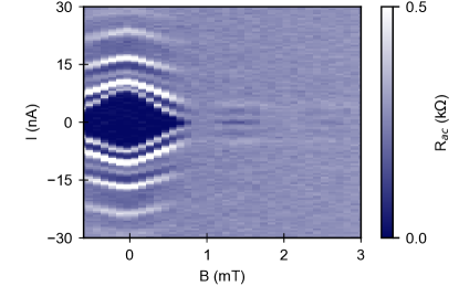
Finally, we apply a perpendicular magnetic field and investigate the differential resistance of the junction, as shown in Fig. 4. Fraunhoffer patterns are evident – with some asymmetry between positive and negative applied bias. The critical current goes to zero twice in the range shown (three lobes) at the field values where an integer multiple of the flux quantum threads through the weak link Tinkham (2004). The measured field at which the critical current is cancelled by currents of opposite direction due to the flux through the junction is mT, which is lower than the expected value given the dimensions of the junction. This discrepancy can be explained either by magnetic flux focusing due to the Meissner effect in the superconducting leads or alternatively by an increased London penetration depth in the thin-film epi-Al. Such variation in the length-scales in thin-film superconductors is not uncommon, having been observed elsewhere Suominen et al. (2017) and, indeed, are an area of active theoretical research. In conclusion, we have demonstrated that Al-mask anodization represents a viable route to nanoscale device fabrication, in particular gate-tunable Josephson junctions in InAs quantum wells. The technique is versatile and likely applicable to various materials.
We thank S. Pauka and M. Cassidy for useful conversations and technical help. This research was supported by the Microsoft Corporation and the Australian Research Council Centre of Excellence for Engineered Quantum Systems (EQUS, CE170100009). The authors acknowledge the facilities as well as the scientific and technical assistance of the Research & Prototype Foundry Core Research Facility at the University of Sydney, part of the Australian National Fabrication Facility.
References
- Kitaev (2001) A. Y. Kitaev, Phys. Usp. 44, 131 (2001).
- Nayak et al. (2008) C. Nayak, S. H. Simon, A. Stern, M. Freedman, and S. D. Sarma, Reviews of Modern Physics 80, 1083 (2008).
- Lutchyn et al. (2010) R. M. Lutchyn, J. D. Sau, and S. D. Sarma, Phys. Rev. Lett. 105, 077001 (2010), arXiv:1002.4033 [cond-mat.supr-con] .
- Oreg et al. (2010) Y. Oreg, G. Refael, and F. von Oppen, Phys. Rev. Lett. 105, 177002 (2010), arXiv:1003.1145 [cond-mat.mes-hall] .
- Mourik et al. (2012) V. Mourik, K. Zuo, S. M. Frolov, S. R. Plissard, E. P. A. M. Bakkers, and L. P. Kouwenhoven, Science 336, 1003 (2012), arXiv:1204.2792 [cond-mat.mes-hall] .
- Kjaergaard et al. (2016) M. Kjaergaard, F. Nichele, H. J. Suominen, M. P. Nowak, M. Wimmer, A. R. Akhmerov, J. A. Folk, K. Flensberg, J. Shabani, C. J. Palmstrøm, and C. M. Marcus, 7 (2016), 10.1038/ncomms12841.
- Hatke et al. (2017) A. Hatke, T. Wang, C. Thomas, G. Gardner, and M. Manfra, Applied Physics Letters 111, 142106 (2017).
- Kroger et al. (1981) H. Kroger, L. Smith, and D. Jillie, Applied Physics Letters 39, 280 (1981).
- Richter et al. (2002) A. Richter, P. Baars, and U. Merkt, 12, 911 (2002).
- Heida et al. (1998) J. Heida, B. Van Wees, T. Klapwijk, and G. Borghs, Physical Review B 57, R5618 (1998).
- Mur et al. (1996) L. Mur, C. Harmans, J. Mooij, J. Carlin, A. Rudra, and M. Ilegems, Physical Review B 54, R2327 (1996).
- Fornieri et al. (2019) A. Fornieri, A. M. Whiticar, F. Setiawan, E. Portolés, A. C. C. Drachmann, A. Keselman, S. Gronin, C. Thomas, T. Wang, R. Kallaher, G. C. Gardner, E. Berg, M. J. Manfra, A. Stern, C. M. Marcus, and F. Nichele, 569, 89 (2019).
- Pauka et al. (2020) S. Pauka, J. Witt, C. Allen, B. Harlech-Jones, A. Jouan, G. Gardner, S. Gronin, T. Wang, C. Thomas, M. Manfra, et al., Journal of Applied Physics 128, 114301 (2020).
- Peng et al. (2016) Y. Peng, F. Pientka, E. Berg, Y. Oreg, and F. von Oppen, Phys. Rev. B 94, 085409 (2016).
- Diggle et al. (1969) J. W. Diggle, T. C. Downie, and C. W. Goulding, Chemical Reviews 69, 365 (1969).
- Mott (1947) N. Mott, Transactions of the faraday society 43, 429 (1947).
- Hunter and Fowle (1954) M. S. Hunter and P. Fowle, JTES 101, 481 (1954).
- (18) T. Tschirky, S. Mueller, C. A. Lehner, S. Fält, T. Ihn, K. Ensslin, and W. Wegscheider, 95, 10.1103/physrevb.95.115304.
- Umansky et al. (1997) V. Umansky, R. de Picciotto, and M. Heiblum, 71, 683 (1997).
- Drachmann et al. (2021) A. C. Drachmann, R. E. Diaz, C. Thomas, H. J. Suominen, A. M. Whiticar, A. Fornieri, S. Gronin, T. Wang, G. C. Gardner, A. R. Hamilton, et al., Physical Review Materials 5, 013805 (2021).
- Feshchenko et al. (2015) A. Feshchenko, L. Casparis, I. Khaymovich, D. Maradan, O.-P. Saira, M. Palma, M. Meschke, J. Pekola, and D. Zumbühl, Physical Review Applied 4, 034001 (2015).
- Suominen et al. (2017) H. Suominen, J. Danon, M. Kjaergaard, K. Flensberg, J. Shabani, C. Palmstrøm, F. Nichele, and C. Marcus, Physical Review B 95, 035307 (2017).
- Mayer et al. (2019) W. Mayer, J. Yuan, K. S. Wickramasinghe, T. Nguyen, M. C. Dartiailh, and J. Shabani, Applied Physics Letters 114, 103104 (2019).
- Kjærgaard et al. (2017) M. Kjærgaard, H. J. Suominen, M. Nowak, A. Akhmerov, J. Shabani, C. Palmstrøm, F. Nichele, and C. M. Marcus, Physical Review Applied 7, 034029 (2017).
- (25) G. E. Blonder, M. Tinkham, and T. M. Klapwijk, 25, 4515.
- Tinkham (2004) M. Tinkham, Introduction to superconductivity (Courier Corporation, 2004).