Thermal-Field Electron Emission from Three-Dimensional
Topological Semimetals
Abstract
A model is constructed to describe the thermal-field emission of electrons from a three-dimensional (D) topological semimetal hosting Dirac/Weyl node(s). The traditional thermal-field electron emission model is generalised to accommodate the D non-parabolic energy band structures in the topological Dirac/Weyl semimetals, such as cadmium arsenide (\chCd3As2), sodium bismuthide (\chNa3Bi), tantalum arsenide (\chTaAs) and tantalum phosphide (\chTaP). Due to the unique Dirac cone band structure, an unusual dual-peak feature is observed in the total energy distribution (TED) spectrum. This non-trivial dual-peak feature, absent from traditional materials, plays a critical role in manipulating the TED spectrum and the magnitude of the emission current. At zero temperature limit, a new scaling law for pure field emission is derived and it is different from the well-known Fowler-Nordheim (FN) law. This model expands the recent understandings of electron emission studied for the Dirac D materials into the D regime, and thus offers a theoretical foundation for the exploration in using topological semimetals as novel electrodes.
I Introduction
Topological Weyl/Dirac semimetals (WSM/DSM)s, a subset of Dirac materials have been studied rapidly over the past decade [1, 2, 3, 4, 5, 6, 7, 8, 9] due to its electronic [10, 11, 12, 13], optical [14, 15, 16, 13] and magnetic [17, 16, 13] properties. The unconventional band structures about its Dirac point have bought about many interesting applications in electronics [18, 19, 20], spintronics [21], photonics [22, 23], nonlinear optics [24, 25, 26] and topological electronics (topotronics) [27]. Apart from these applications, the physics of electron emission from Dirac materials like carbon-based nanomaterials [28, 29, 30] or graphene [31, 32, 33, 34, 35, 36, 37, 38, 39, 40] have also received attentions over the past two decades.
Field-induced electron emission describes the quantum tunnelling of electrons from a material surface into a vacuum under a strong electric field. The most well-known field emission physics is described by the Fowler-Nordheim (FN) based models developed for traditional bulk materials [41, 42, 43]. Compared to the conventional field emitters [44, 45, 46, 47, 48, 49], novel quantum materials exhibit Dirac conic band structure about its Fermi level with non-parabolic energy dispersion [9], and they have also been experimentally shown to exhibit large field enhancement and stable current emission [50, 51, 52]. However, the physics of thermal-field emission of some recently discovered topological solids (such as D Dirac/Weyl semimetals) has not been studied in details, which immediately leads to the following questions: (i) How can the conventional thermal-field emission model be generalized to accommodate the nonparabolic band structure of topological semimetals? (ii) How does the Dirac conic band structure affect the themral-field emission behaviours of D WSM/DSM? (iii) What are the differences between conventional metal and WSM/DSM in terms of their current, voltage and temperature scaling laws at the both field and thermal-field emission regimes?
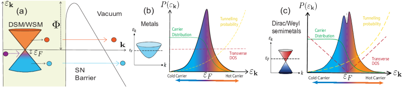
In this paper, we address the above questions by constructing a generalized thermal-field emission model for the newly discovered D DSMs/WSMs. In particular, the total energy distribution (TED) and the emission current density are calculated. Our model applies the Dirac cone approximation for DSMs/WSMs and considers the Schottky-Nordheim (SN) barrier [41, 53] at the material-vacuum interface, as seen in Fig. 1. The electron emission can reside from either the conduction (orange) or valence (blue) bands and are then replenished (purple) at the intrinsic Fermi level, . The differing (linear) energy dispersion from a Dirac cone allows us to study the thermal-field emission of D DSMs/WSMs. For a linear dispersion, we predict an unconventional TED behaviour and a new scaling law at the zero temperature limit, which is different from the FN law. By tuning the applied electric field strength, temperature and Fermi level of a DSM/WSM, we can manipulate the energy profile of TED and the magnitude of the emission current density. These findings can pave the way for the theoretical study of other topological materials, in particular, materials that are described by Dirac cone(s) and Weyl nodes in the band structure, which cannot be modelled by the traditional thermal-field emission models [53].

II Thermal-Field emission models
We consider a generalized thermal-field electron emission model in the form of
| (1) |
where is the electron current density emitted vertically from a surface, is the charge of an electron, is the degeneracy factor, is the Fermi-Dirac distribution function and is the tunnelling probability. The Heaviside step function, , is defined to exclude the electronic states propagating backward in the negative vertical direction. The group velocity along the emitting direction (denoted as ) is
| (2) |
| DSMs/WSMs | (eV) | (eV) | ( m/s) | ( m/s) | |
|---|---|---|---|---|---|
| Cd3As2111References [6, 54, 8, 55] | |||||
| Na3Bi222References [7, 54] | |||||
| TaAs333References [56, 57, 58] | |||||
| TaP444References [56, 58] |
In the following, we define to be pointing in the direction and along the - plane. The tunnelling probability in Eq. 1 can be modelled after the SN barrier model [53, 41] to account for the image charge potential, given by
| (3) |
where is the tunnelling exponent term and is the decay width of the wave function through the barrier, is a Fowler-Nordheim (FN) constant [42] with being the electron mass, is the work function of the material, and is the applied field. The image charge effect can be approximated with the following correction terms: [41]
| (4) |
with , where is the vacuum permittivity.
II.1 Generalized thermal-field emission current density for non-parabolic energy dispersion
To accommodate the non-parabolic energy dispersion, we transform Eq. 1 into an alternative form. We first consider a generic energy dispersion, with and as the energy component transverse and along the tunnelling direction, respectively. By rewriting Eq. 1 in terms of the and the components through , with , we have
| (5) |
where we have defined the energy dispersion factors as
| (6) |
and the following transformation identity is used
Note that is defined. The energy dispersion factors in Eq. 6 play crucial roles in understanding the electron field emission with non-parabolic energy dispersion.
Consider an isotropic D parabolic energy dispersion, where is the electron effective mass and with representing the wave vector component transverse to the emission direction, the total energy is partitioned into the emission component , the transverse component , and . In doing so, Eq. 6 becomes
| (7) |
which is a constant term (independent of and ). Solving Eq. 1 with Eq. 7 will yield the classic Fowler-Nordheim (FN) law for cold field emission, and the Murphy-Good (MG) model for thermal-field emission.
For a non-parabolic (or linear) energy dispersion, we have
| (8) |
For topological Dirac/Weyl semimetals, the quasiparticles around the Dirac point(s) are described by the effective Hamiltonian, where and is the Pauli matrix along and the subscript labels the th Dirac cone [9, 56, 57, 59, 60]. The energy dispersion of these topological semimetals (SM) is
| (9) |
where and . The corresponding energy dispersion factors for non-parabolic dispersion are
| (10) |
where is the Fermi velocity along the direction. This is in stark contrasts to the parabolic dispersion case as shown in Eq. 7 and will lead to a drastically different thermal-field emission characteristics for topological Dirac/Weyl semimetals to be reported below.


II.2 Thermal-field emission current density and total energy distribution from Dirac cones
For an isotropic parabolic energy dispersion, Section II.1 can be simplified as
| (11) |
is the spin degeneracy, , which can be approximately solved to yield the well-known Murphy-Good (MG) thermal-field emission model [53]:
| (12) |
where is the FN constant and is the Boltzmann constant.
The FN plot (for FN scaling) can be obtained by rearranging Eq. 12 such that,
| (13) |
At K (cold field emission), it recovers the classical FN scaling of . Note the component in the logarithm term is a signature of field emission from bulk materials.
In contrast, Section II.1 of a DSM/WSM exhibits a non-trivial difference due to Eq. 10, which can be written as
| (14) |
where is the spin and node degeneracy for each contributing Dirac cone, is the number of contributing Dirac cone(s) to the emission. Section II.2 can be further simplified and numerically solved as
| (15) |
where is a constant with the rest mass of the electron being and the dimensionless tunnelling function is defined as
| (16) |
The FN plot now takes the form of
| (17) |
At K (cold field emission), Section II.2 becomes
| (18) |
where . The scaling law at then becomes
| (19) |
where is negligible in the pure field emission regime. Thus this produces an unexpected scaling of
| (20) |
which is different from the classical FN scaling of for bulk solids with parabolic dispersion.
The energy spectrum of the emitted electrons is determined from the total energy distribution (TED): by considering such that,
| (21) |
where the transverse density of states is , with .
For a parabolic dispersion, the TED takes on a conventional single peak behaviour due to the trivial energy dispersion factors in Eq. 7, which gives us the well-known MG TED in the form of,
| (22) |


On the contrary, Eq. 10 will produce a differing and non-trivial ( and dependence) term in the transverse DOS and the integration, which is
| (23) |
Unlike the parabolic dispersion commonly used for bulk metals in Fig. 1, the linear dispersion and the vanishing density of states of a DSM/WSM portrays a new dual-peak feature in the TED, as illustrated in Fig. 1. This distinctive feature is attributed by the products of three terms in Eq. 21: (green solid line), the integration of (yellow dotted line), and the integration of (red dotted line). The coloured region under the TED graph corresponds to the emitting energy band, where blue/orange represents the emission from the valence/conduction band. The purple region represents the emission around the Fermi level. As seen below, this unconventional behaviour in the TED can be utilised to manipulate the energy profile of the emission process.
III Results and Discussion
III.1 Dual-peak total energy distribution
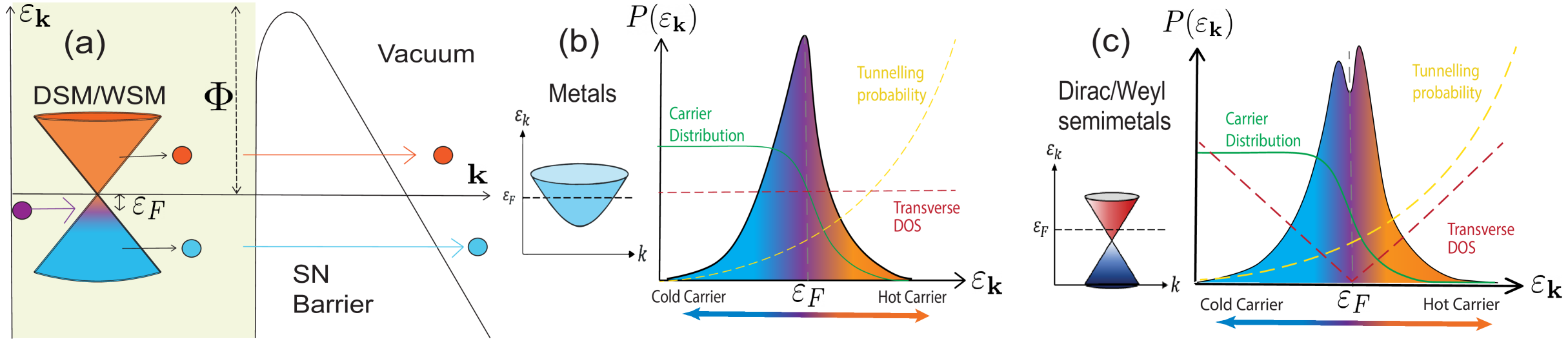
We investigate the appearance of the dual-peak feature in topological semimetals in Fig. 2. The material parameters for the topological semimetals are given in Table 1. In comparison, bulk metals [49, 61, 62] are considered in our calculations: (a) Tungsten \chW with eV and eV; (b) Platinum \chPt with eV and eV. Unlike topological semimetals, materials modelled with a parabolic dispersion like \chW and \chPt do not generate this duel-peak behaviour in its TED for all ranges of , and . This behaviour arises in topological semimetals from in Eq. 23 due to the differing (Dirac conic) band structure embedded in Eq. 10. In contrast, this is not seen for a parabolic dispersion as in Eq. 22 from Eq. 7 and is consistent with Figs. 1 and 1. The dual-peak TED is thus a signature of the Dirac conic band structure.
Furthermore, the dual-peak feature can be generated or removed by regulating the energies of the carriers by changing and . This can be seen by comparing Figs. 2 to 2 ( K , Vnm) and Figs. 2 to 2 ( K, Vnm) against Figs. 2 to 2 ( K, Vnm). The dependency of in Eq. 23 regulates the number of high energy carriers (from the conduction band) as is varied. As the height of the potential barrier is varied through , the dependency of in Eq. 23 makes it easier/harder for the low energy carriers (from the valence band) to tunnel across the surface barrier. Hence, the dual-peak feature can be modulated by tuning the and until the number of high and low energy carriers for emission is similar/vastly different. This feature appears in Fig. 2 for \chCd3As2 (red line), with the peak before/after the Fermi level (red dotted line) termed as the low/high energy peak. Likewise, the dual peaks disappear as is further increased, allowing more low energy carriers to be emitted as shown in \chCd3As2 [Fig. 2]. Thus, the dual-peak feature is not robust against the variation of and .
In addition to and , the dual-peaks can also be created by varying . This can be seen across the columns of Fig. 2, that an increase of introduces more hot carriers. This is supported by Eq. 23, where the term introduce more hot carriers and the term allows the hot carriers to tunnel through easier from increasing . An explicit example can be seen in Figs. 2 and 2 for \chNa3Bi (blue line), where the dual-peak feature appears only after a sufficient increased of . Hence, the plays a vital role in regulating the number of hot carriers for emission, which is crucial in manipulating the dual-peak feature.
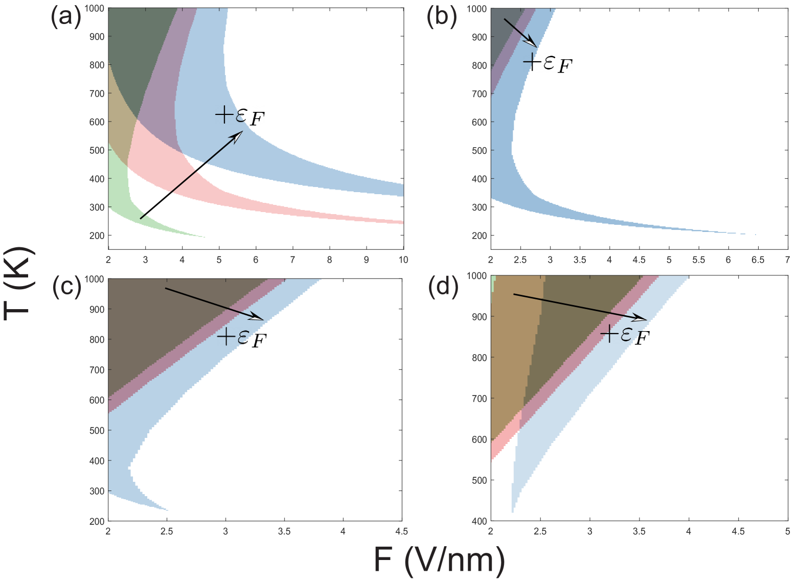
III.2 Susceptibility diagram of the dual-peak TED
In Fig. 3, we further study the mechanism of the dual-peak feature in Fig. 2 as illustrated by increasing in the susceptibility (-) diagram of the dual-peak feature. It can be seen that the dual-peak regions expand and shift with increasing in all four topological semimetals. This is predicted in Eqs. 23 and 2, where the increase in increases the number of high energy carriers. Due to the scarcity of the high energy carriers in the field emission regime, the expansion of the region is expected as the increased number of high energy carriers makes it more conducive to generate the dual-peak feature by the variation of and , which is seen in Figs. 3 and 3 for \chNa3Bi and \chTaAs. The shifting of the regions indicates that the dual-peak feature can be generated or removed at different ranges of and , with an increasing number of high energy carriers by increasing . This is explicitly seen in Figs. 3 and 3 for \chCd3As2 and \chTaP and is supported by the gain or lost of the dual-peak feature in Fig. 2. Thus, the susceptibility diagram pinpoints the parameters to achieve the dual-peak feature, which can be useful in generating a larger emission current density as seen in Fig. 4.
Furthermore, the susceptibility diagram shows that the dual-peak feature can be easily observed for \chCd3As2 with its intrinsic Fermi level, . Not only does \chCd3As2 have the largest green () region, it also have a very noticeable shift in Fig. 3, which is further supported by Fig. 2, where it can exhibits this feature more prominently. This is due to \chCd3As2 having high as compared to the other three topological semimetals. Thus, the susceptibility diagram shows that \chCd3As2 is a suitable candidate amongst these four topological semimetals to observe this dual-peak feature in future experiments.
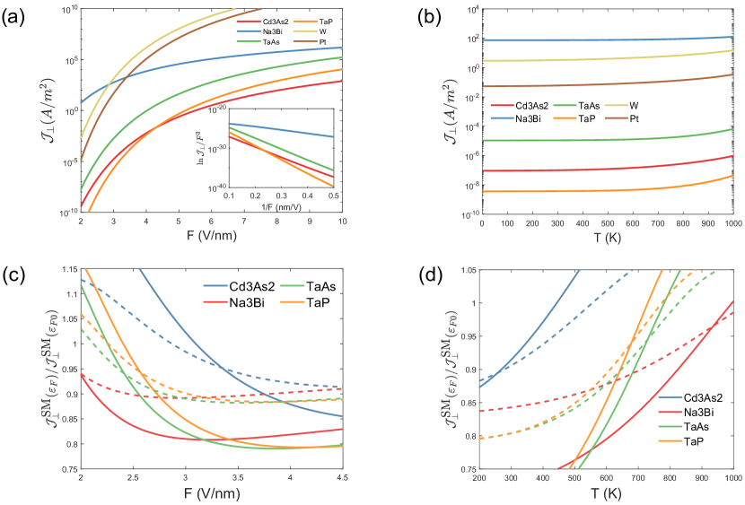
III.3 Emission current density and scaling law
For comparison, the thermal-field emission current density between DSM/WSM [ in Section II.2] and traditional materials with parabolic dispersion [Eq. 12] is plotted in Fig. 4 at K and Fig. 4 Vnm at its intrinsic Fermi level, . Due to the semi-metallic nature of DSMs/WSMs, it is expected that they exhibit a lower emission current density than the metallic emitters due to their limited electronic carrier density. Indeed, we observe that the emission current density () of DSMs/WSMs [\chCd3As2 (red line), \chTaAs (green line) and \chTaP (orange line)] is lower than traditional materials [\chW (yellow line) and \chPt (brown line)] with the exception of \chNa3Bi (blue line) due to its significant lower work function of eV. Such behaviour is expected from Eqs. 12 and II.2 as they share similar and dependence terms in their thermal-field emission current densities.
Interestingly, the inset in Fig. 4 shows that the field emission follows an unconventional scaling of (Eq. 20) for all topological semimetals. The excellent linearity of reveals that DSM/WSM emitter follows an unconventional non-FN scaling not commonly seen in traditional materials.
The effects of the parameters on the ratio of against while varying and are being investigated in Figs. 4 and 4. The ratio dips below for increasing / decreasing . With a lower , it is easier to activate more low energy carriers for emission as compared to a higher with an enlarged conduction band when increasing . Similarly, the reduced number of high energy carriers has a lesser effect on the TED as with a lower , the emission is dominated by low energy carriers. This goes in tandem with the loss of the dual-peak feature, which signifies the dominance of the low energy carriers for as seen either fixing K or Vnm in Fig. 3. Notably, \chNa3Bi exceed in Fig. 4, which is expected as it did not exhibit the dual-peak property with as seen in Figs. 2 and 3. Thus, a higher thermal-field emission current densities can be achieved by either altering or by manipulating the dual-peak feature with the variation of and .
IV Conclusion
In conclusion, we have developed a thermal-field emission model for D Dirac semimetal (DSM) and Weyl semimetal (WSM) with a linear Dirac conic energy dispersion such as \chCd3As2, \chNa3Bi, \chTaAs, and \chTaP. Our results predict the existence of a non-trivial dual-peak feature in the total energy distribution (TED) and a new scaling law, which is absent in an electron field emitter composed of traditional metals with conventional D parabolic energy band structure. The characteristics of this dual-peak feature are unique to DSM/WSM and may serve as a smoking gun signature for the Dirac conic energy dispersion in topological semimetals. Furthermore, the relatively low work function of \chNa3Bi can be beneficial for field emission application due to its high emission current density. \chCd3As2 with its sufficiently high Fermi level (in spite of high work function), is also a suitable candidate for achieving a larger emission current density by exploiting the high sensitivity of the dual-peak feature with the variation of , and . Finally, we remark that our model does not capture secondary effects, such as field-induced topological phase transition [9, 13, 63], band bending [64], space charge [65, 66], and Fermi velocity shifting [58, 67]. Such effects could be included in future works to investigate their roles on the thermal-field emission characteristics of D DSM/WSM.
V Acknowledgements
This work is funded by MOE Tier 2 (2018-T2-1-007). Y.S.A. acknowledges the support of SUTD Startup Research Grant (Project No. SRT3CI21163). W.J.C. acknowledge MOE PhD RSS.
Appendix A Derivation of TED and emission current density with linear (non-parabolic) dispersion for a DSM/WSM
The generalised emission electrical current density from a D bulk electron emitter with a linear (non-parabolic) dispersion is shown in Section II.1 of Section II as
| (24) |
where the superscript indicates a linear dispersion. Inserting Eq. 10 into Section II.1 garner us Section II.2 such that,
| (25) |
Without loss of generality, we can discard the Dirac node label, by specifying a Dirac node. This allow us to temporary remove the summation, which can be placed back at the end.
The integration then gives:
| (26) |
where the approximation can be made as the emission takes place near the Fermi level.
Due to the absolute function in , we have to consider both the and regime, such that for ,
| (27) |
and for ,
| (28) |
Hence, we can combine them into a dimensionless tunnelling function such that
| (29) |
where
This can be done as the limits of Eqs. 27 and A at are equal and can be easily verified. Hence, the integration becomes
| (30) |
Next for the and integration,
| (31) |
where and the identity, and was used.
This changes Section II.2 into Section II.2
| (32) |
where the SM represents the emission current density of a topological semimetal, is a constant, with being the rest mass of the electron.
References
- Son et al. [2006] Y.-W. Son, M. L. Cohen, and S. G. Louie, Energy Gaps in Graphene Nanoribbons, Phys. Rev. Lett. 97, 216803 (2006), arXiv:0611602 [cond-mat] .
- Oka and Aoki [2009] T. Oka and H. Aoki, Photovoltaic Hall effect in Graphene, Phys. Rev. B 79, 081406 (2009), arXiv:0807.4767 .
- Xu et al. [2011] G. Xu et al., Chern Semimetal and the Quantized Anomalous Hall Effect in \chHgCr2Se4, Phys. Rev. Lett. 107, 186806 (2011).
- Lv et al. [2015] B. Q. Lv et al., Observation of Weyl nodes in \chTaAs, Nat. Phys. 11, 724 (2015).
- McCormick et al. [2017] T. M. McCormick, I. Kimchi, and N. Trivedi, Minimal models for topological Weyl semimetals, Phys. Rev. B 95, 075133 (2017).
- Liu et al. [2014a] Z. K. Liu et al., A stable three-dimensional topological Dirac semimetal \chCd3As2, Nat. Mater. 13, 677 (2014a).
- Liu et al. [2014b] Z. K. Liu et al., Discovery of a Three-Dimensional Topological Dirac Semimetal, \chNa3Bi, Science 343, 864 (2014b).
- Crassee et al. [2018] I. Crassee et al., D Dirac semimetal \chCd3As2: A review of material properties, Phys. Rev. Mater. 2, 120302 (2018), arXiv:1810.03726 .
- Wehling et al. [2014] T. Wehling, A. Black-Schaffer, and A. Balatsky, Dirac materials, Adv. Phys. 63, 1 (2014), arXiv:1405.5774 .
- McCann and Koshino [2013] E. McCann and M. Koshino, The electronic properties of bilayer graphene, Reports Prog. Phys. 76, 056503 (2013), arXiv:1205.6953 .
- Wan et al. [2011] X. Wan, A. M. Turner, A. Vishwanath, and S. Y. Savrasov, Topological semimetal and Fermi-arc surface states in the electronic structure of pyrochlore iridates, Phys. Rev. B 83, 205101 (2011).
- Xiong et al. [2016] J. Xiong et al., Anomalous conductivity tensor in the Dirac semimetal \chNa3Bi, EPL (Europhysics Lett. 114, 27002 (2016), arXiv:1502.06266 .
- Wang et al. [2017a] S. Wang et al., Quantum transport in Dirac and Weyl semimetals: a review, Adv. Phys. X 2, 518 (2017a).
- Lasia and Brey [2014] M. Lasia and L. Brey, Optical properties of magnetically doped ultrathin topological insulator slabs, Phys. Rev. B. 90, 075417 (2014), arXiv:1404.7040 .
- Xu et al. [2016] B. Xu et al., Optical spectroscopy of the Weyl semimetal TaAs, Phys. Rev. B 93, 121110 (2016).
- Polatkan et al. [2020] S. Polatkan et al., Magneto-Optics of a Weyl Semimetal beyond the Conical Band Approximation: Case Study of \chTaP, Phys. Rev. Lett. 124, 176402 (2020), arXiv:1912.07327 .
- Choi et al. [2011] Y. H. Choi et al., Transport and magnetic properties of \chCr-, \chFe-, \chCu-doped topological insulators, J. Appl. Phys. 109, 07E312 (2011).
- Li et al. [2016] P.-B. Li, Z.-L. Xiang, P. Rabl, and F. Nori, Hybrid Quantum Device with Nitrogen-Vacancy Centers in Diamond Coupled to Carbon Nanotubes, Phys. Rev. Lett. 117, 015502 (2016), arXiv:1606.02998 .
- Zhu et al. [2017] C. Zhu et al., A robust and tuneable mid-infrared optical switch enabled by bulk Dirac fermions, Nat. Commun. 8, 14111 (2017).
- Wang et al. [2017b] Q. Wang et al., Ultrafast Broadband Photodetectors Based on Three-Dimensional Dirac Semimetal \chCd3As2, Nano Lett. 17, 834 (2017b).
- Šmejkal et al. [2018] L. Šmejkal, Y. Mokrousov, B. Yan, and A. H. MacDonald, Topological antiferromagnetic spintronics, Nat. Phys. 14, 242 (2018).
- Khanikaev et al. [2013] A. B. Khanikaev et al., Photonic topological insulators, Nat. Mater. 12, 233 (2013).
- Yu et al. [2019] Y.-Z. Yu et al., Photonic topological semimetals in bianisotropic metamaterials, Sci. Rep. 9, 18312 (2019).
- Lim et al. [2020a] J. Lim, Y. S. Ang, F. J. García de Abajo, I. Kaminer, L. K. Ang, and L. J. Wong, Efficient generation of extreme terahertz harmonics in three-dimensional Dirac semimetals, Phys. Rev. Res. 2, 043252 (2020a).
- Zhang et al. [2019] T. Zhang, K. J. A. Ooi, W. Chen, L. K. Ang, and Y. Sin Ang, Optical Kerr effect and third harmonic generation in topological Dirac/Weyl semimetal, Opt. Express 27, 38270 (2019).
- Lim et al. [2020b] J. Lim, K. J. A. Ooi, C. Zhang, L. K. Ang, and Y. S. Ang, Broadband strong optical dichroism in topological Dirac semimetals with Fermi velocity anisotropy, Chinese Phys. B 29, 077802 (2020b).
- Wang et al. [2020] A.-Q. Wang, X.-G. Ye, D.-P. Yu, and Z.-M. Liao, Topological Semimetal Nanostructures: From Properties to Topotronics, ACS Nano 14, 3755 (2020).
- Hofmann et al. [2003] S. Hofmann, C. Ducati, B. Kleinsorge, and J. Robertson, Direct growth of aligned carbon nanotube field emitter arrays onto plastic substrates, Appl. Phys. Lett. 83, 4661 (2003).
- Liang and Chen [2008] S.-D. Liang and L. Chen, Generalized Fowler-Nordheim Theory of Field Emission of Carbon Nanotubes, Phys. Rev. Lett. 101, 027602 (2008).
- Zhou et al. [2019] S. Zhou et al., Ultrafast Field-Emission Electron Sources Based on Nanomaterials, Adv. Mater. 31, 1 (2019).
- Giubileo et al. [2018] F. Giubileo et al., Field Emission from Carbon Nanostructures, Appl. Sci. 8, 526 (2018).
- Chen et al. [2017] L. Chen et al., Graphene field emitters: A review of fabrication, characterization and properties, Mater. Sci. Eng. B 220, 44 (2017).
- Sun et al. [2011] S. Sun, L. K. Ang, D. Shiffler, and J. W. Luginsland, Klein tunnelling model of low energy electron field emission from single-layer graphene sheet, Appl. Phys. Lett. 99, 013112 (2011).
- Ang et al. [2017] Y. Ang, S.-J. Liang, and L. Ang, Theoretical modeling of electron emission from graphene, MRS Bull. 42, 505 (2017).
- Wei et al. [2012] X. Wei, Y. Bando, and D. Golberg, Electron emission from individual graphene nanoribbons driven by internal electric field, ACS Nano 6, 705 (2012).
- Liang and Ang [2015] S.-J. Liang and L. K. Ang, Electron thermionic emission from graphene and a thermionic energy converter, Phys. Rev. Applied 3, 014002 (2015).
- Ang et al. [2018] Y. S. Ang, H. Y. Yang, and L. K. Ang, Universal scaling laws in schottky heterostructures based on two-dimensional materials, Phys. Rev. Lett. 121, 056802 (2018).
- Ang et al. [2019] Y. S. Ang, Y. Chen, C. Tan, and L. K. Ang, Generalized high-energy thermionic electron injection at graphene interface, Phys. Rev. Applied 12, 014057 (2019).
- Huang et al. [2017] S. Huang, M. Sanderson, Y. Zhang, and C. Zhang, High efficiency and non-Richardson thermionics in three dimensional Dirac materials, Appl. Phys. Lett. 111, 1 (2017).
- Ang et al. [2021] Y. S. Ang, L. Cao, and L. K. Ang, Physics of electron emission and injection in two‐dimensional materials: Theory and simulation , InfoMat , 502 (2021).
- Forbes [2006] R. G. Forbes, Simple good approximations for the special elliptic functions in standard Fowler-Nordheim tunneling theory for a Schottky-Nordheim barrier, Appl. Phys. Lett. 89, 113122 (2006).
- Forbes and Deane [2007] R. G. Forbes and J. H. Deane, Reformulation of the standard theory of Fowler–Nordheim tunnelling and cold field electron emission, Proc. R. Soc. A Math. Phys. Eng. Sci. 463, 2907 (2007).
- Jensen and Cahay [2006] K. L. Jensen and M. Cahay, General thermal-field emission equation, Appl. Phys. Lett. 88, 10 (2006).
- Swanson et al. [1966] L. W. Swanson, L. C. Crouser, and F. M. Charbonnier, Energy exchanges attending field electron emission, Phys. Rev. 151, 327 (1966).
- Dionne et al. [2009] M. Dionne, S. Coulombe, and J.-L. Meunier, Energy exchange during electron emission from carbon nanotubes: Considerations on tip cooling effect and destruction of the emitter, Phys. Rev. B 80, 085429 (2009).
- Chung [1994] M. S. Chung, Energy exchange processes in electron emission at high fields and temperatures, J. Vac. Sci. Technol. B Microelectron. Nanom. Struct. 12, 727 (1994).
- Binh et al. [1996] V. T. Binh, N. Garcia, and S. Purcell, Electron Field Emission from Atom-Sources: Fabrication, Properties, and Applications of Nanotips, in Adv. Imaging Electron Phys., Vol. 95 (Elsevier, 1996) pp. 63–153.
- Young [1959] R. D. Young, Theoretical Total-Energy Distribution of Field-Emitted Electrons, Phys. Rev. 113, 110 (1959).
- Gadzuk and Plummer [1973] J. W. Gadzuk and E. W. Plummer, Field Emission Energy Distribution (FEED), Rev. Mod. Phys. 45, 487 (1973).
- Lee et al. [2012] J. Lee et al., High-performance field emission from a carbon nanotube carpet, Carbon N. Y. 50, 3889 (2012).
- de Jonge et al. [2005] N. de Jonge, M. Allioux, J. T. Oostveen, K. B. K. Teo, and W. I. Milne, Optical Performance of Carbon-Nanotube Electron Sources, Phys. Rev. Lett. 94, 186807 (2005).
- Li et al. [2012] L. Li, W. Sun, S. Tian, X. Xia, J. Li, and C. Gu, Floral-clustered few-layer graphene nanosheet array as high performance field emitter, Nanoscale 4, 6383 (2012).
- Murphy and Good [1956] E. L. Murphy and R. H. Good, Thermionic Emission, Field Emission, and the Transition Region, Phys. Rev. 102, 1464 (1956).
- Jenkins et al. [2016] G. S. Jenkins, C. Lane, B. Barbiellini, A. B. Sushkov, R. L. Carey, F. Liu, J. W. Krizan, S. K. Kushwaha, Q. Gibson, T.-r. Chang, H.-t. Jeng, H. Lin, R. J. Cava, A. Bansil, and H. D. Drew, Three-dimensional Dirac cone carrier dynamics in \chNa3Bi and \chCd3As2., Phys. Rev. B 94, 085121 (2016).
- Huang et al. [2020] Z. Huang et al., High responsivity and fast UV–vis–short-wavelength IR photodetector based on \chCd3As2 / \chMoS2 heterojunction, Nanotechnology 31, 064001 (2020).
- Lee et al. [2015] C.-C. Lee et al., Fermi surface interconnectivity and topology in Weyl fermion semimetals \chTaAs, \chTaP, \chNbAs, and \chNbP, Phys. Rev. B 92, 235104 (2015).
- Chi et al. [2017] S. Chi et al., Ultra-broadband photodetection of weyl semimetal taas up to infrared 10 m range at room temperature (2017), arXiv:1705.05086 [cond-mat.mtrl-sci] .
- Grassano et al. [2018] D. Grassano, O. Pulci, A. Mosca Conte, and F. Bechstedt, Validity of Weyl fermion picture for transition metals monopnictides TaAs, TaP, NbAs, and NbP from ab initio studies, Sci. Rep. 8, 3534 (2018).
- Du et al. [2020] Z. Du et al., Field emission behaviors of CsPbI 3 nanobelts, J. Mater. Chem. C 8, 5156 (2020).
- Berry et al. [2020] T. Berry, L. A. Pressley, W. A. Phelan, T. T. Tran, and T. M. McQueen, Laser-Enhanced Single Crystal Growth of Non-Symmorphic Materials: Applications to an Eight-Fold Fermion Candidate, Chem. Mater. 32, 5827 (2020).
- Nicolaou and Modinos [1975] N. Nicolaou and A. Modinos, Band-structure effects in field-emission energy distributions in tungsten, Phys. Rev. B 11, 3687 (1975).
- Bordoloi and Auluck [1983] A. K. Bordoloi and S. Auluck, Electronic structure of platinum, J. Phys. F Met. Phys. 13, 2101 (1983).
- Armitage et al. [2018] N. P. Armitage, E. J. Mele, and A. Vishwanath, Weyl and Dirac semimetals in three-dimensional solids, Rev. Mod. Phys. 90, 015001 (2018), arXiv:1705.01111 .
- Litovchenko et al. [2007] V. Litovchenko, A. Evtukh, et al., Electron field emission from narrow band gap semiconductors (InAs), Semicond. Sci. Technol. 22, 1092 (2007).
- Abdul Khalid et al. [2016] K. A. Abdul Khalid, T. J. Leong, and K. Mohamed, Review on Thermionic Energy Converters, IEEE Trans. Electron Devices 63, 2231 (2016).
- Zhang et al. [2021] P. Zhang, Y. S. Ang, A. L. Garner, Á. Valfells, J. W. Luginsland, and L. K. Ang, Space–charge limited current in nanodiodes: Ballistic, collisional, and dynamical effects, J. Appl. Phys. 129, 100902 (2021).
- Baba et al. [2019] Y. Baba, Á. Díaz-Fernández, E. Díaz, F. Domínguez-Adame, and R. A. Molina, Electric field manipulation of surface states in topological semimetals, Phys. Rev. B 100, 165105 (2019), arXiv:1907.06516 .