Impact of surface and laser-induced noise on the spectral stability of implanted nitrogen-vacancy centers in diamond
Abstract
Scalable realizations of quantum network technologies utilizing the nitrogen vacancy center in diamond require creation of optically coherent NV centers in close proximity to a surface for coupling to optical structures. We create single NV centers by 15N ion implantation and high-temperature vacuum annealing. Origin of the NV centers is established by optically detected magnetic resonance spectroscopy for nitrogen isotope identification. Near lifetime-limited optical linewidths ( 60 MHz) are observed for the majority of the normal-implant (7∘, 100 nm deep) 15NV centers. Long-term stability of the NV- charge state and emission frequency is demonstrated. The effect of NV-surface interaction is investigated by varying the implantation angle for a fixed ion-energy, and thus lattice damage profile. In contrast to the normal implant condition, NVs from an oblique-implant (85∘, 20 nm deep) exhibit substantially reduced optical coherence. Our results imply that the surface is a larger source of perturbation than implantation damage for shallow implanted NVs. This work supports the viability of ion implantation for formation of optically stable NV centers. However, careful surface preparation will be necessary for scalable defect engineering.
I Introduction
Nitrogen-vacancy (NV) point defects in diamond combine optical addressability [1, 2, 3] with long spin coherence times [4], making them promising candidates for quantum networking [5, 6]. NV centers in diamond have been used to demonstrate essential ingredients for quantum networks in recent experiments,including on-demand remote entanglement generation [7, 8], coherent control of multiple nearby nuclear spin memories[9] and memory-enhanced quantum communication[10, 8]. For networking schemes, optical coherence and photon collection efficiency are key figures of merit. Nanophotonic integration of NV centers has demonstrated potential for high collection efficiency and scalable integration [11, 12, 13, 14] and thus should enable the scaling of quantum entanglement networks. The small mode volume needed for significant photonic coupling requires localization of NV centers to within tens of nanometers from diamond surfaces. Hybrid materials platforms [13, 15], which minimize diamond fabrication, utilize evanescent coupling require NV centers in even closer surface proximity. Nitrogen ion (N+) implantation followed by high-temperature annealing is a commonly utilized process for targeted spatial localization of NV centers for device integration. However, recent published results by van Dam et al. [16] and Kasperczyket al. [17] determined that centers with high optical coherence created by N+ implantation and annealing are predominantly formed by implantation-induced vacancies diffusing and combining with native nitrogen. As vacancies are relatively mobile at annealing temperatures [18, 19, 20, 21], this result implies loss of localization and precludes deterministic photonic device integration.
The optical coherence of shallow NV centers can suffer degradation from two sources; (1) charge traps formed in the bulk from the implantation and annealing process and (2) charge traps associated with the surface or sub-surface of diamond. Ionization of charge traps produces a dynamically changing electric field which couples to the different dipole moments of the ground and excited states of the NV centers[22, 23, 15, 24]. This effect manifests as linewidth broadening and spectral diffusion of the NV optical transitions. Since the prescription for each possible source is quite different, it is important to identify the relevant culprit. Here we show that for 100 nm implant depth, it is possible to create 15NV centers with typical optical transition linewidths 60 MHz. Additionally, the long-term spectral stability of the NV transitions to within 200 MHz is demonstrated. For this implant condition, given the average NV-surface distance, we expect bulk sources to dominate optical decoherence. The observed spectral stability implies bulk sources can be overcome.
Encouraged by the 100 nm implantation results, we explore the possibility of implanting coherent centers closer to the surface. Shallower centers allow for enhanced optical coupling [13] for hybrid materials devices. We create NV centers at 20 nm by changing the angle of implantation as opposed to varying the energy of implantation. Hence, the local damage profile around an NV center is similar to the 100 nm implantation condition, merely rotated relative to the surface. Here we find that the optical linewidths are orders of magnitude larger and are accompanied by decreased spectral stability.
Combined, these observations strongly imply that the proximity to the diamond surface is the dominant source of optical decoherence, and that the bulk implantation damage profile is not the limiting factor for shallow implanted NV centers.
II Experiment
II.1 Samples
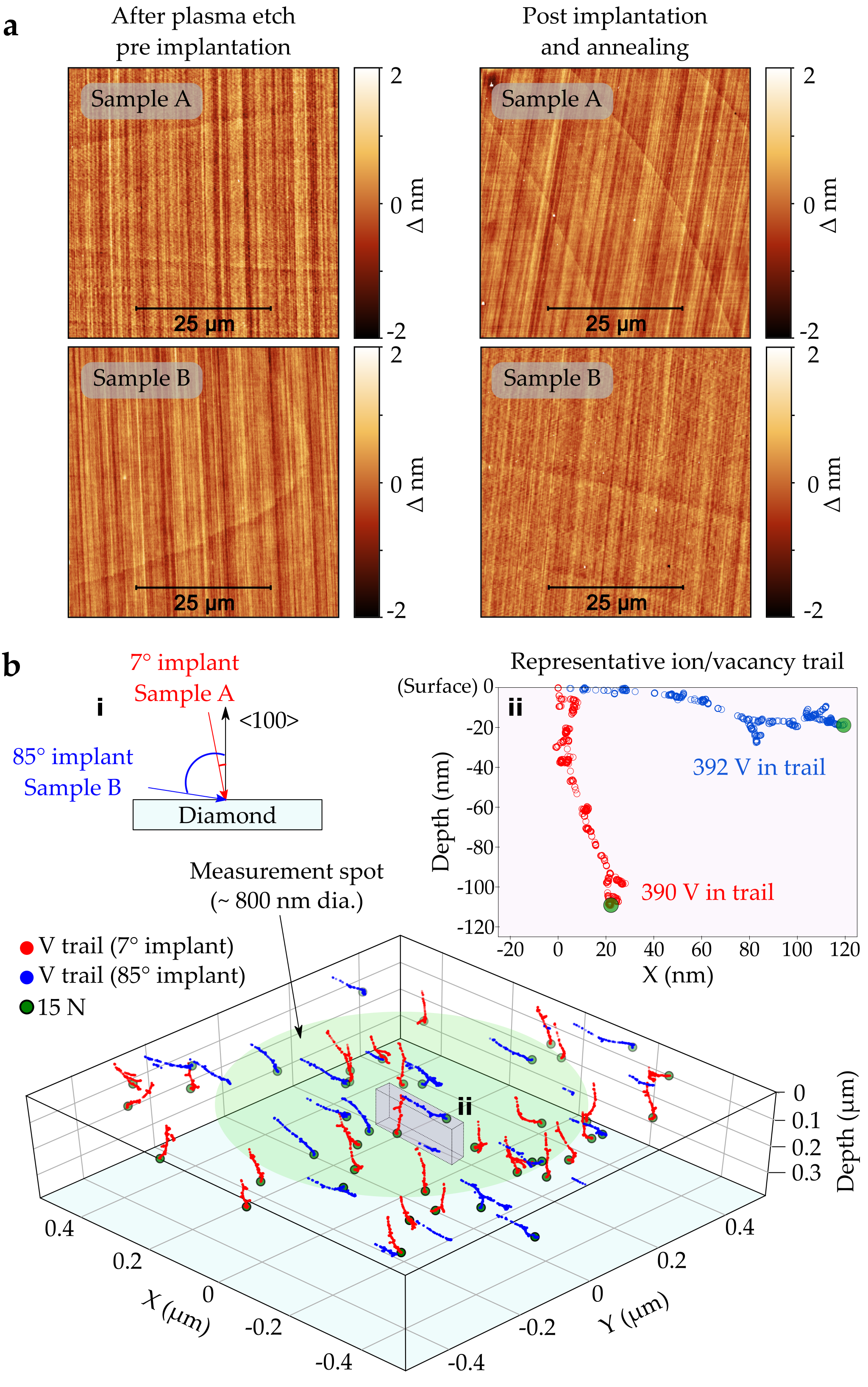
In our primary study, to elucidate the effect of the surface on the optical properties of implanted NV centers, we utilize two identical chemical vapor deposition diamonds samples A and B (Element Six, electronic grade, N 1 ppb, B 1 ppb), with 100 surfaces. As purchased, the diamond surfaces are polished to less than 1 nm RMS surface roughness. Both samples are processed identically unless stated otherwise. First, we etch away 5 µm from the surface using plasma reactive-ion etching to remove polishing damage [23]. We take the following precautions to avoid micro-masking that is a common occurrence during diamond etching: At each step the diamonds are cleaned in a boiling 1:1:1 mixture of H2SO4, H2NO3 and HClO4 at 260 ∘C for one hour to remove organic contaminants and graphitic carbon [23]. A sapphire carrier wafer is utilized to prevent silicon contamination of the diamond surface during the etch [25]. We utilize a two step Ar/Cl plasma (physical etching via sputtering) followed by O2 plasma (chemical etching via oxidation) process to remove any deposited material that may result in micro-masking (process details are provided in Appendix A). The total etch duration is 45 min of Ar/Cl2 and 20 min of O2 etching. Post processing, both diamonds have nearly identical surface morphology with sample A (B) exhibiting 0.63 (0.43) nm RMS roughness (Fig. 1a).
We implant both samples A (B) with 15N at identical energies and effective beam dosages of 85 keV and 3e9 ions/cm2. The implantation angle for samples A and B are 7∘ and 85∘ respectively. We model the effect of the different ion incidence angles on the implantation profile using the Stopping and Range of Ions in Matter (SRIM) code [26]. For sample A (B), the average depth of the 15N atoms is 10020 (2113) nm below the surface. Although the effective beam dosage is the identical for both samples, approximately 41% of the incident ions are back-scattered for sample B. This back-scattering is a geometric consequence of rotating the damage profile relative to the surface, such that some of the scattered ions escape the diamond surface. Hence the final 15N density in sample B is predicted to have 60% the density of sample A.
The samples are vacuum annealed at 1.410-7 mbar, 1100 ∘C for two hours with long ramp times as described in Ref. [23, 16]. This is followed by a short two hour anneal at 435 ∘C under O2 flow to oxygen terminate the surface and stabilize the negative charge state [27, 28] of the near-surface NV centers.
In addition, we characterize four supplemental diamond NV implantation samples (C-F) to support the reproducibility of the primary study. These diamond substrates have identical specifications (Element Six, electronic grade) but are sourced from different growth runs. Pre-implantation, all samples are processed as detailed in this section. The specifics of implantation/annealing conditions for each sample are provided in the table accompanying Fig. 4.
II.2 Measurements
A confocal microscope comprising a 532 nm DPSS laser and 60X (NA=0.7) objective lens is used to scan over 80x80 µm2 areas using a piezo stage. A polarizing beamsplitter with an automated half-wave plate is used in the excitation path to preferentially excite a given NV orientation.
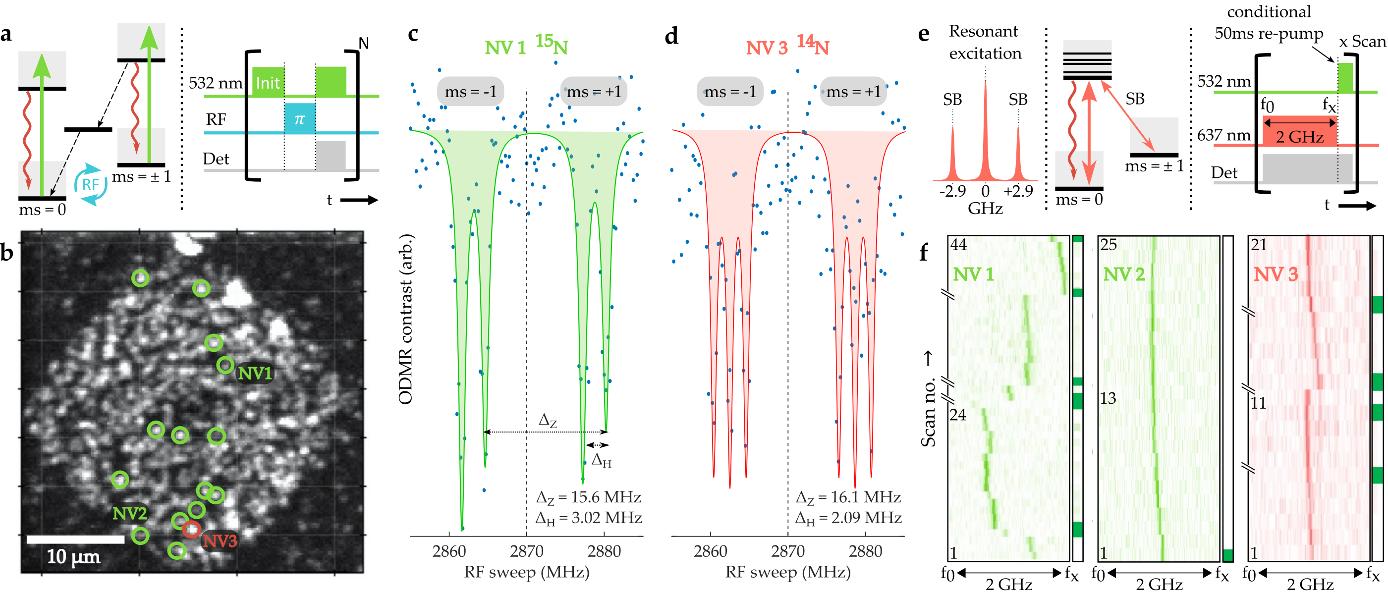
To identify the nitrogen isotope associated with each NV center, we use optically-detected magnetic resonance (ODMR) spectroscopy. For an NV in the ms = 1 ground spin-sublevel, reduced photoluminescence (PL) is observed upon off-resonant excitation due a small likelihood ( 20%) of relaxation through the dark inter-system crossing transition [29, 30] (dotted line, Fig. 2a). The samples are placed in a weak magnetic field ( 5 G) that splits the ms = 1 ground spin-sublevels. RF excitation is delivered via a small copper loop (radius 0.3 mm) suspended 50µm above the diamond sample. A short (5 µs) off-resonant 532 nm laser pulse initializes the NV into the ms = 0 spin state. Next, a radio-frequency (RF) -pulse (0.8 µs) rotates the NV spin state before time resolved NV PL is recorded during the subsequent short (5 µs) readout laser pulse. The -pulse area is initially calibrated by performing a Rabi experiment. The pulse sequence is repeated while sweeping the RF driving frequency over all the NV ground state spin transitions. The resulting two (three) dip PL intensity spectrum corresponds to the 15N (14N) NV-N ground state hyperfine interaction [1, 31], indicating that the NV incorporates an implanted or grown-in nitrogen atom (Fig. 2c,d). ODMR spectra are measured at room-temperature for randomly sampled NV centers in the implantation region (Fig. 2b) and fit to a three (14NV) or two (15NV) dip Lorentzian. The positions of the sampled NV centers are recorded. The samples are then cooled to 12 K in a close cycle cryostat for spectral characterization of the selected NV centers.
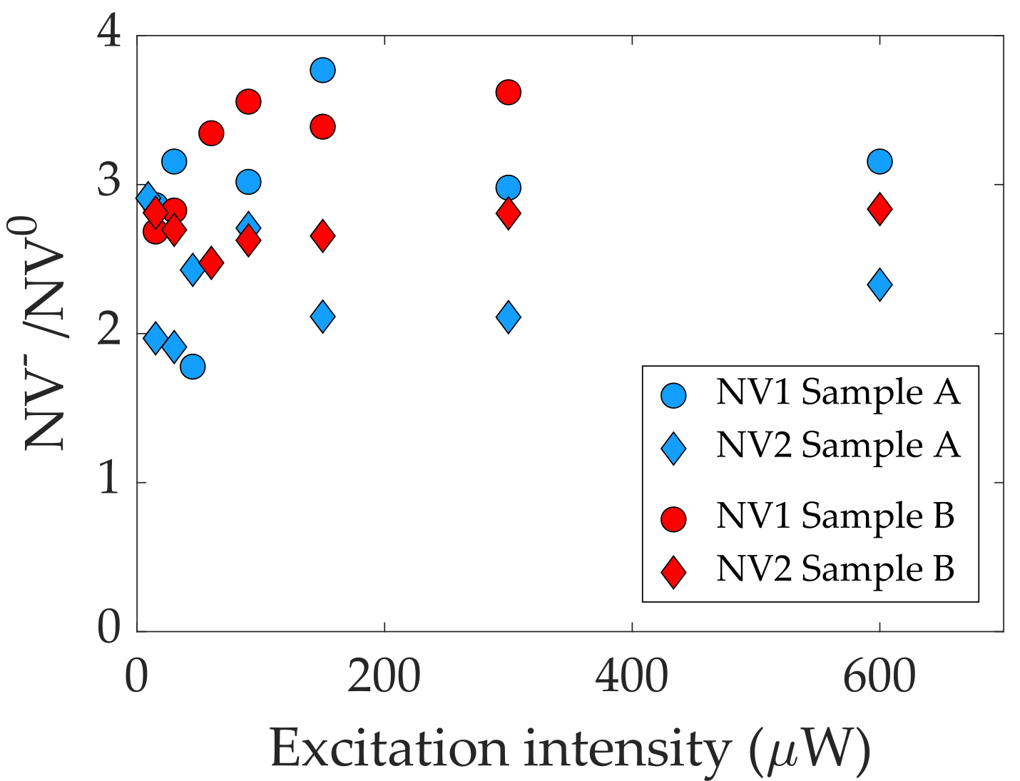
Low-temperature NV- PL spectra under CW 532 nm excitation provides the inhomogeneous distribution of the ZPL transition (Fig. 5) arising from variations in the local strain and electric field environment of individual centers. The NV charge state ratio (NV-/NV0) is also recorded as a function of the excitation intensity for a subset of centers (Appendix C). Additionally, high resolution photoluminescence excitation (PLE) spectroscopy provides insight into the optical coherence and temporal spectral stability of individual NV centers. In PLE measurements, a narrow-band tunable laser is scanned across the NV- ZPL while collecting the NV- phonon-sideband PL (650 nm to 800 nm) (Fig. 2e). The resonant laser and accompanying 2.9 GHz sidebands simultaneously drive the {ms=0, ms=1} {Ex, Ey} transitions [32, 33, 34].
From the PLE spectra we collect statistics on the ZPL single-scan linewidth as well as the scan-to-scan variation in the ZPL frequency. During PLE we can sometimes observe a loss of the NV- PL signal due to ionization to the NV0 state; to reinitialize into the NV- charge state we apply a short low power 532 nm repump pulse (50 ms) between scans (as indicated by the green markers in Fig. 2f). The interval between repump pulses is an additional indicator of the stability of NV- charge state.
III Correlated ODMR and PLE spectroscopy
On sample A, ODMR was performed on 32 NV centers with 26 centers identified as 15NV, one as 14NV; remaining five NVs could not be conclusively identified. Similarly, on sample B, ODMR was performed on 38 NV centers with 27 centers identified as 15NV, two as 14NV; the remaining nine NVs could not be identified. The observed total NV density for sample A (B) is 1.2/ µm2 (0.3/ µm2) corresponds to an implantation conversion yield of 4 % (1 %). For both these samples, no grown-in NVs were observed in a 80 µm 80 µm area at a depth of 50 µm implying very low native Ns density [35]. Considering the natural abundance of 15N (0.4 %) and the 15NV/14NV ratio for both samples ( = 26, = 13.5), it is clear that for our diamond substrates and implantation conditions that NV formation incorporating implanted nitrogen is favored.
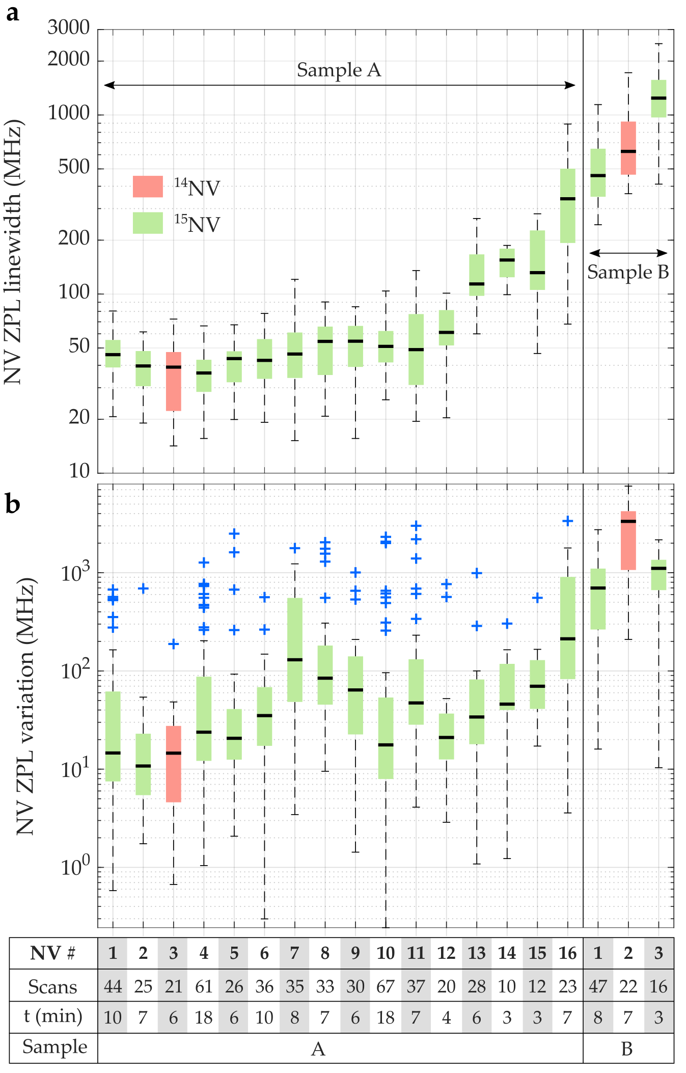
First let us consider sample A. The single NV low-temperature ZPL spectra under off-resonant 532 nm excitation is typically spectrometer resolution limited ( 0.021 nm). PLE spectroscopy reveals that both 15N and 14N centers typically exhibit near lifetime-limited linewidths. A sequence of laser scans over a span of 10 minutes (each scan is 4 to 8 s in duration) gives us a median linewidth of 60 MHz for 12 out of 16 centers (Fig.3a). This linewidth is computed by individually fitting each scan to a Lorentzian. The laser intensity is set between 30 to 60 nW with a scan rate of 1 to 2.5 GHz/s. A linewidth power dependence measurement was performed on two centers to ensure that the observed linewidths are not significantly power-broadened in our intensity range. The PLE results are summarized in Fig. 3a; the solid boxes mark the fitted linewidths between first and third quartile. This interquartile range is an indicator of spectral diffusion () of the NV ZPL during a single resonant laser scan (on the timescale of ms).
Additionally, by tracking the ZPL frequency between scans, we can characterize the long term spectral stability (on the timescale of s). We calculate this spectral variation () by recording the change in ZPL frequency between subsequent scans (Fig.3b). Here, we emphasize that an off-resonant re-pump pulse is only applied when no NV PL is detected (i.e. NV- has ionized to NV0) emulating emerging NV quantum networking protocols [8, 7]. The median spectral variation is typically 100 MHz, for long periods (60 to 300 s) between re-pumps. We observe that most 15NV centers experience large spectral jumps ( 500 MHz) after an off-resonant re-pump pulse. These jumps occur in 95% of the re-pump events. In Fig.3b, the blue markers indicate re-pump triggered spectral jumps. This is the only metric where we see a clear advantage for the 14NV also observed on sample A (Fig. 3, red). It is unclear at this time if the re-pump triggered perturbation originates at the surface (with the single 14NV lying deeper within the sample) or from local implantation damage. Nevertheless, it may still be mitigated with the use of a low-power resonant NV0 re-pump pulse [36].
Sample B reveals a different story, the low-temperature ZPL spectra under off-resonant 532 nm excitation for individual NV centers is much broader (0.02 to 0.25 nm;). Given that the lattice damage profile is similar to sample A, this spectral broadening could be attributed to rapid fluctuations of surface charges effectively Stark-tuning the NV centers within the exposure duration of the spectra. Such rapid ZPL fluctuations make resonant 637 nm PLE measurements very challenging. Of the six NV centers randomly sampled, only three showed PLE signal. All three NV centers (two 15N and one 14N) exhibit broad median linewidths (0.5 GHz to 1.2 GHz) and increased spectral variability (Fig. 3).
Finally, we confirm that the NV- charge state is preferred across the full range of optical powers (15 to 600 µW of 532 nm excitation) for both samples A and B (Appendix C).
IV Automated spectroscopy
To corroborate the data from our primary samples (A, B), we present automated ODMR, PLE and low-temperature off-resonant PL spectroscopy datasets on four other samples (C to F). Our automation procedure allows us to sample hundreds of NV centers, however we are unable to track individual NV centers between PL, PLE and ODMR datasets. Details of the automated measurement protocol are provided in Appendix B.
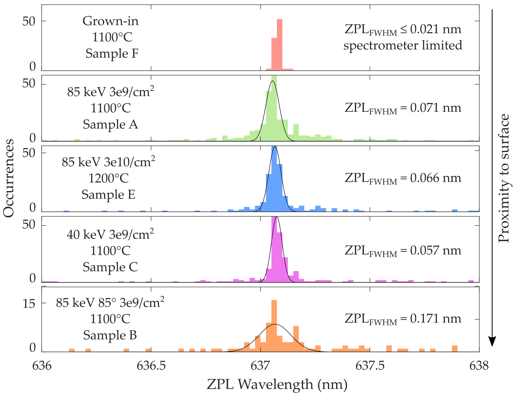
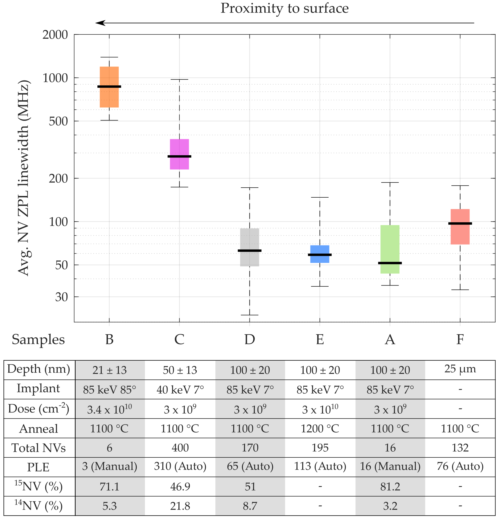
First, let us consider samples D and E with similar implant conditions (15N, 85 keV 7∘) to sample A. Uncorrelated ODMR measurements on sample D show most centers are 15N. The measured average ZPL linewidth distribution (Fig. 4) of hundreds of NV centers, tracks well with the dataset from sample A, indicating reproducibility of narrow-linewidth 15NV centers. In the ideal case, the linewidth of NV centers created through ion implantation and annealing would be equal to the linewidth observed in background NV centers distributed throughout the sample. No background NV centers could be identified in either samples (A, B) and a low density prohibited automated measurements in samples (C, D, E). Automated PLE measurements on native NV centers 25 µm within sample F, a similar electronic-grade sample that has undergone high-temperature annealing (with no implantation), serve as our reference. From the data presented in Fig. 4, the average NV linewidth distribution of all the 85 keV, 7∘ implant samples are in agreement with the reference sample.
Next, we examine the shallow implantation samples. The average ZPL linewidth distribution in Fig. 4, shows that both the shallow NV samples C (40 keV 7∘) and B (85 keV 85∘) exhibit decreased optical coherence. This is despite the fact that initial implantation damage for sample C is significantly lower compared to samples A, D and E (85 keV 7∘). We can use the average number of vacancies (V) generated per implanted ion trail as an analogue for local lattice damage. From SRIM [26] simulations, sample C incorporates 203 V/ion whereas samples A, B, D and E incorporate 390 V/ion. This provides further evidence that the broadening seen for the shallow implants is unrelated to the implantation damage at these energies and dosages and instead is a result of charge traps associated with the surface.
In addition, low-temperature PL spectra (off-resonant excitation) from a large number of NV centers provides the inhomogeneous ZPL distribution (Fig. 5). Regardless of the variations in the total implant damage (V/µm3), the inhomogeneous NV ZPL distributions are similar for samples A, C and E (Gaussian fit FWHM = 52.5 GHz, 42.1 GHz and 48.8 GHz respectively). The grown-in NV centers exhibit a narrower ZPL spread (FWHM 15.4 GHz, spectrometer resolution limited). Finally, the ZPL distribution for sample B is much broader (FWHM = 126 GHz) than any of our other samples. A comparison suggests that there is still a small amount of residual strain remaining in the implantation samples.
V Conclusion
Lattice damage from the ion-implantation process introduces localized perturbations of the defect environment. Our result with the 85 keV 7∘ implant samples indicates much of this damage can be annealed out for an 15NV created directly from an implanted nitrogen. We observe that 15NV centers exhibit long periods of spectral stability, wherein their spectral characteristics are akin to optically coherent grown-in NV centers. The implanted 15NV and grown-in centers exhibit comparable median optical linewidths. However, we do see distinct advantages for grown-in centers in terms of behavior under off-resonant green re-pump and inhomogeneous ZPL distribution. For 15NV centers, green re-pump pulses used to reinitialize the NV charge state introduce large spectral variation ( 500 MHz). This behavior hints at why our 15NV linewidths are qualitatively different from van Dam et al. [16] and Kasperczyk et al. [17]. They utilize re-pump pulses every scan, which we can see would cause linewidth broadening into GHz. In fact, an analysis considering only the PLE scans immediately after the repump pulse indicates our results in Sample A are consistent with the 400 nm 400 keV 15N implanted sample in van Dam et al. Further studies are necessary to pin down the source of the re-pump triggered variation. Nevertheless, for the 15NV centers, observation of long periods of spectral stability between re-pumps shows promise for implementation of quantum networks with integrated photonic devices.
Further, we show that this optical stability rapidly degrades with increasing proximity to the diamond surface, corroborating measurements by Ref. [24] of NV centers in thin diamond membranes which showed strong correlation of reduced NV spectral stability with decreasing membrane thickness, not accompanied by a change in the NV strain environment. Ref. [24] suggests that the additional NV dephasing may be attributed the Ar/Cl2 plasma etch process even for micron-scale thick samples. Our past work has seen a similar effect on implanted centers [14]. Indeed, Ref. [37] show that 1 µm thin diamond membranes with improved diamond surface quality (etched by a soft graded O2 plasma) can host NV centers with narrow linewidths.
Our conclusions fit into a larger narrative regarding the source of degradation of other properties near surfaces as well, such as NV . Recent work by Ref. [38] correlating the reduction of NV within 20 nm of the surface has shown that the for NV center within 10 nm of the surface can be enhanced an order of magnitude by preparing diamonds with smoother surfaces and well-ordered oxygen termination. Further work would need to be done to determine whether the spin-bath responsible for degradation is related to the charge traps we infer in our optical measurements, however both suggest that solving the surface interaction problem is more important than fixing residual implantation damage.
Acknowledgements.
We would like to thank N.P. de Leon and R. Hanson for helpful discussions; undergraduate REU students K. Crane and M. Chamberlain for assistance with measurement automation; E.R. Schmidgall for help with fabrication process development and pre-implantation etching of our diamond samples. This material is based upon work supported by the National Science Foundation under ECCS-1807566. The diamond samples were processed at the Washington Nanofabrication Facility, a National Nanotechnology Coordinated Infrastructure (NNCI) site at the University of Washington which is supported in part by funds from the National Science Foundation award NNCI-1542101.Appendix A Plasma processing details
We utilize an Oxford Plasmalab-100/ICP-180 etcher. The samples are sandwiched between two sapphire slides held in place with a drop of Crystalbond-509 (applied as a solution in acetone) on a 100 mm sapphire carrier wafer. The total etch duration is broken up into multiple etch cycles involving 5 min of plasma processing followed by a 3 min no plasma cooldown phase. This ensures the diamond sample is maintained near the processing temperature. The samples remain in the etcher through the entire two step process. The etch parameters are provided in table. 1.
Appendix B Automated spectroscopy procedure
Confocal scans with off-resonant 532 nm excitation are utilized to generate an NV PL intensity map of the region of interest. First, individual NV centers are identified by image processing (peak prominence detection) and their x, y and z piezo positions are registered. The linearly polarized excitation is optimized for one set of NV orientations. ODMR, PLE and low-temperature off-resonant spectra datasets are acquired by iterating through the registered NV centers. During the iteration process, at each registered center the piezo x, y and z positioners are cycled through three PL optimization sweeps to correct for microscope drift. Before proceeding with pulsed ODMR at RT, a Rabi experiment is manually performed to extract the RF pi-pulse specifications for the dataset. This is followed by ODMR performed at RT.
| Parameter | Ar/Cl2 | O2 |
|---|---|---|
| RF power (W) | 240 | 50 |
| ICP power (W) | 320 | 1500 |
| DC bias (V) | 530 | 150 |
| Chamber Pressure (mTorr) | 9 | 25 |
| Ar flow (sccm) | 32 | 0 |
| Cl2 flow (sccm) | 20 | 0 |
| O2 flow (sccm) | 0 | 20 |
| Chuck temperature (∘C) | 15 | 15 |
| Total duration (min) | 45 | 20 |
Next, the samples are cooled in a closed cycle 10 K cryostat (Janis CCS-XG-M/204N) for the PLE dataset. Because we switch microscopes between automated ODMR (RT) and PLE (LT), the datasets are not correlated. Hence for our primary correlated dataset (samples A, B) consecutive ODMR and PLE measurements were performed manually on the same microscope. For each center, PLE is performed in two steps, coarse and fine scans. First, the coarse scans utilize the full range of a New Focus velocity tunable laser ( 85 GHz) to identify the ZPL frequency. Then a set of 30 scans are performed across the identified ZPL (scan range = 5 GHz) with high resolution (=10 MHz). For samples C, D and F, a 50 ms off-resonant re-pump is applied at the end of each scan. For sample E, re-pump pulse is only applied if no NV PL is observed during scan (i.e. indicating NV has ionized to the neutral charge state). In post-processing, each scan is fitted to a Lorentzian, and the average FWHM of the fits is calculated. During analysis, a set of preset criteria (peak intensity, fitted FWHM, fit shape) are used to discard scans with ionization events. The average FWHM distribution thus computed for all NV centers in the dataset is shown in Fig. 4. No sideband or microwave driving was used for the automated PLE datasets.
Finally, off-resonant ZPL spectra is collected for registered NV centers with a 1800g Princeton Acton 2750 spectrometer (=0.0208 nm). Here, if multiple peaks are observed in individual spectra, they are recorded as independent peaks. We do not distinguish the different transitions associated with the NV excited state spin sublevels. To identify the excited state structure with confidence would require a confirmation of a single NV in the excitation spot, obtained via a photon autocorrelation measurement, which is time intensive and not currently feasible with the automated process.
Appendix C NV-/NV0 charge state ratio
To determine the preferred NV charge state, we look at the ratio of NV- and NV0 ZPL intensities at =637 and 575 nm respectively. The NV spectra are measured under off-resonant excitation at 12 K. NV- charge state is predominant throughout the observed excitation range (NV-/NV0 typically 2) for implanted NV centers in both samples A and B.
References
- Doherty et al. [2013] M. W. Doherty, N. B. Manson, P. Delaney, F. Jelezko, J. Wrachtrup, and L. C. Hollenberg, Physics Reports 528, 1 (2013).
- Jelezko and Wrachtrup [2006] F. Jelezko and J. Wrachtrup, physica status solidi (a) 203, 3207 (2006).
- Robledo et al. [2011] L. Robledo, L. Childress, H. Bernien, B. Hensen, P. F. Alkemade, and R. Hanson, Nature 477, 574 (2011).
- Abobeih et al. [2018] M. H. Abobeih, J. Cramer, M. A. Bakker, N. Kalb, M. Markham, D. J. Twitchen, and T. H. Taminiau, Nature Communications 9, 2552 (2018).
- Kimble [2008] H. J. Kimble, Nature 453, 1023 (2008).
- Wehner et al. [2018] S. Wehner, D. Elkouss, and R. Hanson, Science 362 (2018).
- Humphreys et al. [2018] P. C. Humphreys, N. Kalb, J. P. J. Morits, R. N. Schouten, R. F. L. Vermeulen, D. J. Twitchen, M. Markham, and R. Hanson, Nature 558, 268 (2018).
- Pompili et al. [2021] M. Pompili, S. L. Hermans, S. Baier, H. K. Beukers, P. C. Humphreys, R. N. Schouten, R. F. Vermeulen, M. J. Tiggelman, L. dos Santos Martins, B. Dirkse, et al., Science 372, 259 (2021).
- Bradley et al. [2019] C. Bradley, J. Randall, M. Abobeih, R. Berrevoets, M. Degen, M. Bakker, M. Markham, D. Twitchen, and T. Taminiau, Physical Review X 9, 031045 (2019).
- Kalb et al. [2017] N. Kalb, A. A. Reiserer, P. C. Humphreys, J. J. Bakermans, S. J. Kamerling, N. H. Nickerson, S. C. Benjamin, D. J. Twitchen, M. Markham, and R. Hanson, Science 356, 928 (2017).
- Schröder et al. [2016] T. Schröder, S. L. Mouradian, J. Zheng, M. E. Trusheim, M. Walsh, E. H. Chen, L. Li, I. Bayn, and D. Englund, Journal of the Optical Society of America B 33, B65 (2016).
- Wan et al. [2020] N. H. Wan, T.-J. Lu, K. C. Chen, M. P. Walsh, M. E. Trusheim, L. De Santis, E. A. Bersin, I. B. Harris, S. L. Mouradian, I. R. Christen, et al., Nature 583, 226 (2020).
- Gould et al. [2016] M. Gould, E. R. Schmidgall, S. Dadgostar, F. Hatami, and K.-M. C. Fu, Physical Review Applied 6, 011001 (2016).
- Chakravarthi et al. [2020] S. Chakravarthi, P. Chao, C. Pederson, S. Molesky, A. Ivanov, K. Hestroffer, F. Hatami, A. W. Rodriguez, and K.-M. C. Fu, Optica 7, 1805 (2020).
- Schmidgall et al. [2018] E. R. Schmidgall, S. Chakravarthi, M. Gould, I. R. Christen, K. Hestroffer, F. Hatami, and K.-M. C. Fu, Nano Letters 18, 1175 (2018).
- van Dam et al. [2019] S. B. van Dam, M. Walsh, M. J. Degen, E. Bersin, S. L. Mouradian, A. Galiullin, M. Ruf, M. IJspeert, T. H. Taminiau, R. Hanson, and D. R. Englund, Physical Review B 99, 161203 (2019).
- Kasperczyk et al. [2020] M. Kasperczyk, J. Zuber, A. Barfuss, J. Kölbl, V. Yurgens, S. Flågan, T. Jakubczyk, B. Shields, R. Warburton, and P. Maletinsky, Physical Review B 102, 075312 (2020).
- Santori et al. [2009] C. Santori, P. E. Barclay, K.-M. C. Fu, and R. G. Beausoleil, Physical Review B 79, 125313 (2009).
- Davies et al. [1992] G. Davies, S. C. Lawson, A. T. Collins, A. Mainwood, and S. J. Sharp, Physical Review B 46, 13157 (1992).
- Breuer and Briddon [1995] S. J. Breuer and P. R. Briddon, Physical Review B 51, 6984 (1995).
- Hu et al. [2002] X. J. Hu, Y. B. Dai, R. B. Li, H. S. Shen, and X. C. He, Solid State Communications , 4 (2002).
- Acosta et al. [2012] V. M. Acosta, C. Santori, A. Faraon, Z. Huang, K.-M. C. Fu, A. Stacey, D. A. Simpson, K. Ganesan, S. Tomljenovic-Hanic, A. D. Greentree, S. Prawer, and R. G. Beausoleil, Physical Review Letters 108, 206401 (2012).
- Chu et al. [2014] Y. Chu, N. de Leon, B. Shields, B. Hausmann, R. Evans, E. Togan, M. J. Burek, M. Markham, A. Stacey, A. Zibrov, A. Yacoby, D. Twitchen, M. Loncar, H. Park, P. Maletinsky, and M. Lukin, Nano Letters 14, 1982 (2014).
- Ruf et al. [2019] M. Ruf, M. IJspeert, S. van Dam, N. de Jong, H. van den Berg, G. Evers, and R. Hanson, Nano Letters 19, 3987 (2019).
- Lee et al. [2008] C. Lee, E. Gu, M. Dawson, I. Friel, and G. Scarsbrook, Diamond and Related Materials 17, 1292 (2008).
- Ziegler et al. [2010] J. F. Ziegler, M. D. Ziegler, and J. P. Biersack, Nuclear Instruments and Methods in Physics Research Section B: Beam Interactions with Materials and Atoms 268, 1818 (2010).
- Fu et al. [2010] K.-M. C. Fu, C. Santori, P. E. Barclay, and R. G. Beausoleil, Applied Physics Letters 96, 121907 (2010).
- Yamano et al. [2017] H. Yamano, S. Kawai, K. Kato, T. Kageura, M. Inaba, T. Okada, I. Higashimata, M. Haruyama, T. Tanii, K. Yamada, S. Onoda, W. Kada, O. Hanaizumi, T. Teraji, J. Isoya, and H. Kawarada, Japanese Journal of Applied Physics 56, 04CK08 (2017).
- Goldman et al. [2015] M. L. Goldman, M. W. Doherty, A. Sipahigil, N. Y. Yao, S. D. Bennett, N. B. Manson, A. Kubanek, and M. D. Lukin, Physical Review B 91, 165201 (2015).
- Tetienne et al. [2012] J.-P. Tetienne, L. Rondin, P. Spinicelli, M. Chipaux, T. Debuisschert, J.-F. Roch, and V. Jacques, New Journal of Physics 14, 103033 (2012).
- Yamamoto et al. [2014] T. Yamamoto, S. Onoda, T. Ohshima, T. Teraji, K. Watanabe, S. Koizumi, T. Umeda, L. P. McGuinness, C. Muller, B. Naydenov, F. Dolde, H. Fedder, J. Honert, M. L. Markham, D. J. Twitchen, J. Wrachtrup, F. Jelezko, and J. Isoya, PHYSICAL REVIEW B , 6 (2014).
- Santori et al. [2006] C. Santori, P. Tamarat, P. Neumann, J. Wrachtrup, D. Fattal, R. G. Beausoleil, J. Rabeau, P. Olivero, A. D. Greentree, S. Prawer, F. Jelezko, and P. Hemmer, Physical Review Letters 97, 247401 (2006).
- Tamarat et al. [2008] P. Tamarat, N. B. Manson, J. P. Harrison, R. L. McMurtrie, A. Nizovtsev, C. Santori, R. G. Beausoleil, P. Neumann, T. Gaebel, F. Jelezko, P. Hemmer, and J. Wrachtrup, New Journal of Physics 10, 045004 (2008).
- Fu et al. [2009] K.-M. C. Fu, C. Santori, P. E. Barclay, L. J. Rogers, N. B. Manson, and R. G. Beausoleil, Physical Review Letters 103, 256404 (2009).
- Edmonds et al. [2012] A. M. Edmonds, U. F. S. D’Haenens-Johansson, R. J. Cruddace, M. E. Newton, K.-M. C. Fu, C. Santori, R. G. Beausoleil, D. J. Twitchen, and M. L. Markham, Physical Review B 86, 035201 (2012).
- Siyushev et al. [2013] P. Siyushev, H. Pinto, M. Vörös, A. Gali, F. Jelezko, and J. Wrachtrup, Physical Review Letters 110, 167402 (2013).
- Lekavicius et al. [2019] I. Lekavicius, T. Oo, and H. Wang, Journal of Applied Physics 126, 214301 (2019).
- Sangtawesin et al. [2019] S. Sangtawesin, B. L. Dwyer, S. Srinivasan, J. J. Allred, L. V. Rodgers, K. De Greve, A. Stacey, N. Dontschuk, K. M. O’Donnell, D. Hu, D. A. Evans, C. Jaye, D. A. Fischer, M. L. Markham, D. J. Twitchen, H. Park, M. D. Lukin, and N. P. de Leon, Physical Review X 9, 031052 (2019).