Competing superconductivity and charge-density wave in Kagome metal CsV3Sb5: evidence from their evolutions with sample thickness
Abstract
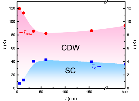
Recently superconductivity and topological charge-density wave (CDW) were discovered in the Kagome metals V3Sb5 ( = Cs, Rb, and K), which have an ideal Kagome lattice of vanadium. Here we report resistance measurements on thin flakes of CsV3Sb5 to investigate the evolution of superconductivity and CDW with sample thickness. The CDW transition temperature decreases from 94 K in bulk to a minimum of 82 K at thickness of 60 nm, then increases to 120 K as the thickness is further reduced to 4.8 nm (about five monolayers). Since the CDW order in CsV3Sb5 is quite three-dimensional (3D) in the bulk sample, the non-monotonic evolution of with reducing sample thickness can be explained by a 3D to 2D crossover around 60 nm. Strikingly, the superconducting transition temperature shows an exactly opposite evolution, increasing from 3.64 K in the bulk to a maximum of 4.28 K at thickness of 60 nm, then decreasing to 0.76 K at 4.8 nm. Such exactly opposite evolutions provide strong evidence for competing superconductivity and CDW, which helps us to understand these exotic phases in V3Sb5 Kagome metals.
The recently discovered V-based Kagome metals, V3Sb5 ( = Cs, Rb, and K), have stimulated great interest in the field of condensed matter physics Rb-K-Cs ; KVSb-Z2 ; RbVSb-SC ; CsV3Sb5-Z2 . These compounds, consisting ideal Kagome lattice of vanadium coordinated by antimony, show superconductivity with superconducting transition temperatures () of 2.5, 0.92, and 0.93 K for = Cs, Rb, and K, respectively CsV3Sb5-Z2 ; KVSb-Z2 ; RbVSb-SC . Besides superconductivity, CDW transitions are revealed in the normal states at 78–104 K for V3Sb5 by X-ray Diffraction (XRD) and scanning tunnelling microscopy (STM) measurements CsV3Sb5-Z2 ; KVSb-Z2 ; RbVSb-SC ; topological_charge_order_KVSb . The angle-resolved photoemission spectroscopy (ARPES) experiemnts point out a topological surface state with multiple Dirac nodal points close to the Fermi level, suggesting that V3Sb5 can be categorized as topological Kagome metals Rb-K-Cs ; CsV3Sb5-Z2 ; KVSb-Z2 .
Furthermore, the STM study revealed a topological charge order in KV3Sb5 with chiral anisotropy topological_charge_order_KVSb , which may cause the giant anomalous Hall effect and a possibility of unconventional superconductivity topological_charge_order_KVSb ; anomalous Hall effect . Indeed, nodal superconductivity and a pressure-induced double dome superconductivity were found by the ultralow-temperature thermal conductivity and high-pressure resistance measurements in CsV3Sb5 SYLiCsVSb . Unconventional strong-coupling superconductivity in these V-based superconductors was also suggested by Josephson STM Strong-coupling . Although the penetration depth and nuclear magnetic resonance (NMR) measurements claimed -wave superconductivity Nodeless superconductivity ; s-wave superconductivity , the subsequent ultralow-temperature STM demonstrated both nodal and nodaless gaps for CsV3Sb5 with multiple Fermi surfaces Multiband superconductivity ; Fermi surface mapping . The exact locations of the gap nodes still need to be identified. In this context, the Kagome metal V3Sb5 provides a great platform to study the interplay of superconductivity, CDW, and topological band structure.
Previously, the superconducting dome under low pressure has already indicated the competition between superconductivity and CDW in V3Sb5 SYLiCsVSb ; J.-G. Cheng ; Z. Yang ; X. Chen ; Pressure-KVSb . In this Letter, we investigate the evolution of superconductivity and CDW with sample thickness in the mechanically exfoliated CsV3Sb5 thin flakes by electrical transport measurement. Two non-monotonic evolutions are revealed, and the one for CDW can be explained by a 3D to 2D crossover around 60 nm. It is striking that the two evolutions are exactly opposite for superconductivity and CDW, demonstrating the competition between them in CsV3Sb5.
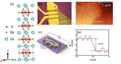
Single crystals of CsV3Sb5 were grown by the self-flux method CsV3Sb5-Z2 ; SYLiCsVSb . Thin flakes of CsV3Sb5 were prepared by an Al2O3-assisted exfoliation method Al2O3 . Al2O3 thin film with thickness ranging from 60 to 100 nm was deposited by thermally evaporating Al under an oxygen pressure of 10-2 Pa on the freshly prepared surface of the bulk CsV3Sb5 single crystal. Then the Al2O3 film was picked up with a thermal release tape, along with pieces of CsV3Sb5 thin flakes separated from the bulk. The Al2O3/CsV3Sb5 stack was subsequently released onto a piece of polydimethylsiloxane (PDMS) upon heating, with the CsV3Sb5 side in contact with the PDMS surface. Next the PDMS was stamped onto a substrate and was peeled away, leaving the Al2O3 film covered with CsV3Sb5 thin flakes on the substrate. Figure 1(b) displays an optical image of CsV3Sb5 thin flake on Al2O3 film supported on a 300 nm SiO2/Si substrate. Then the electrodes were fabricated on the CsV3Sb5 thin flake with direct metal deposition through stencil masks. All the devices were fabricated in an argon atmosphere with O2 and H2O content kept below 0.5 parts per million to avoid sample degradation.
The thickness of the CsV3Sb5 thin flakes was determined by Atomic Force Microscopy (AFM) (Park NX10). The resistance measurements of the thin flakes were performed in a physical properties measurement system (PPMS, Quantum Design) and a 3He refrigerator. All the loading processes out of the glove box were done within one minute to prevent sample from degradation.


As plotted in Fig. 1(a), CsV3Sb5 consists an ideal Kagome lattice of vanadium coordinated by antimony, with the alkali-metal atoms of Cs intercalated between each layer. The lattice parameters are = = 5.4949(3) Å and = 9.3085(5) Å Rb-K-Cs . The single crystal can be easily exfoliated to tens of nanometers by using conventional scotch tape and PDMS films, however such method is difficult to obtain even thinner flakes of CsV3Sb5 sample. With the help of Al2O3, high-quality CsV3Sb5 single crystal can be exfoliated to a few nanometers so that our study can go down to several monolayers. A typical optical image of a CsV3Sb5 thin flake device is shown in Fig. 1(b). Transparent Al2O3 on SiO2/Si substrate manifests green because of diffraction. The yellow part on the Al2O3 is the sample area. A standard four-probe method is used in the resistance measurement. The schematic device structure is plotted in Fig. 1(c). The thickness of the sample was determined by AFM in the selected area marked by red box in Fig. 1(b), along the white line which crosses the edge of the sample in AFM image shown in Fig. 1(d). The AFM measurement gives the thickness of this flake is about 4.8 nm (Fig. 1(e)), corresponding to five monolayers.
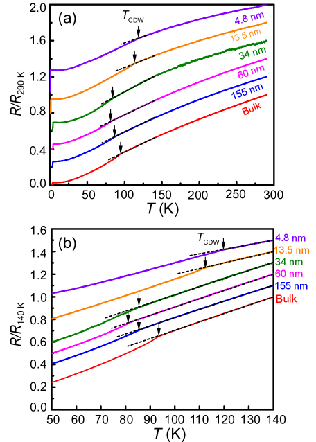
Temperature dependence of the resistance for CsV3Sb5 thin flakes with various thickness, from bulk single crystal to 4.8 nm, are shown in Fig. 2. The data are normalized by the values at 290 and 140 K for (a) and (b), respectively. The curves are vertically shifted for clarity. The arrows mark the CDW transition temperature . For the bulk single crystal, 94 K is consistent with previous report CsV3Sb5-Z2 . With decreasing of the thickness, decreases from 94 K in bulk to a minimum of 82 K at thickness of 60 nm, then increases to 120 K as the thickness is further reduced to 4.8 nm (about five monolayers). Such a non-monotonic evolution of with sample thickness in CsV3Sb5 is quite unusual. To our knowledge, only VSe2 was reported to manifest this kind of non-monotonic thickness dependent of VSe2 . It was attributed to the crossover in the Fermi surface topology from 3D to 2D around 20 nm VSe2 . For bulk CsV3Sb5, 2 2 2 superstructure 2*2*2 and 2 2 4 Fermi surface mapping superstructure were reported, by means of X-ray diffraction, suggesting 3D CDW. Therefore, the non-monotonic evolution of with sample thickness in CsV3Sb5 may be also due to a crossover from 3D to 2D around 60 nm. Note that 60 nm is actually quite thick, far from the 2D limit.

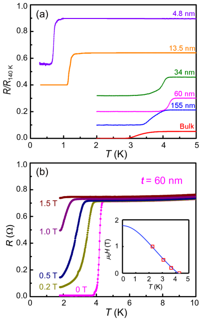
Figure 3(a) plots the low-temperature resistance below 5 K, to show the superconducting transitions. The superconducting transition temperature is defined as the 10% drop of the normal-state resistance. It is found that the first increases from 3.64 K in bulk to a maximum of 4.28 K in the 60 nm sample, then decreases to 0.76 K in the 4.8 nm sample. To confirm that the resistance drop in the 60 nm sample is an enhanced superconducting transition, various magnetic fields are applied, as seen in Fig. 3(b). The resistance drop is suppressed with increasing magnetic field, confirming that it is a superconducting transition. The temperature dependence of upper critical field 0 is plotted in the insets of Fig. 3(b). The data can be well fitted by the Ginzburg-Landau (GL) formula 0()= 0(0)(1-(/)2)/(1+(/)2), giving 0(0) 1.78 T. This value is much higher than that of bulk single crystal SYLiCsVSb . It is worthy to note that the superconducting transition become sharper with the decreasing of the sample thickness.
Based on above resistance measurements of CsV3Sb5 thin flakes, the evolutions of and are plotted in Fig. 4. One can see that shows an exactly opposite evolution, compared with that of . Such exactly opposite evolutions provide strong evidence for competing superconductivity and CDW in CsV3Sb5.

In summary, we investigate the dimensionality effect on superconductivity and CDW of the new Kagome metal CsV3Sb5 by electrical transport measurements. The opposite non-monotonic evolutions of superconductivity and CDW with the sample thickness give strong evidence for competing superconductivity and CDW. The non-monotonic evolution of with reducing sample thickness can be explained by a 3D to 2D crossover around 60 nm. More theoretical calculations and experimental works are needed to clarify the underlying physics of this kind of competition.
This work was supported by the Natural Science Foundation of China (Grant No. 12034004), the Ministry of Science and Technology of China (Grant No.: 2016YFA0300503), and the Shanghai Municipal Science and Technology Major Project (Grant No. 2019SHZDZX01). Y. F. Guo was supported by the Major Research Plan of the National Natural Science Foundation of China (No. 92065201) and the Program for Professor of Special Appointment (Shanghai Eastern Scholar). H. C. Lei was supported by National Natural Science Foundation of China (Grant No. 11822412 and 11774423), the Ministry of Science and Technology of China (Grant No. 2018YFE0202600 and 2016YFA0300504), and Beijing Natural Science Foundation (Grant No. Z200005).
B. Q. Song, X. M. Kong, W. Xia, and Q. W. Yin contributed equally to this work.
† E-mail: hleiruc.edu.cn
‡ E-mail: guoyfshanghaitech.edu.cn
♯ E-mail: yangxiaofanfudan.edu.cn
∗ E-mail: shiyanlifudan.edu.cn
References
- (1) B. R. Ortiz, L. C. Gomes, J. R. Morey, M. Winiarski, M. Bordelon, J. S. Mangum, I. W. H. Oswald, J. A. Rodriguez-Rivera, J. R. Neilson, S. D. Wilson, E. Ertekin, T. M. McQueen, and E. S. Toberer, New Kagome prototype materials: discovery of KV3Sb5, RbV3Sb5, and CsV3Sb5. Phys. Rev. Mater. 3, 094407 (2019).
- (2) E. M. Kenney, M. J. Graf, S. M. L. Teicher, R. Seshadri, and S. D. Wilson, Superconductivity in 2 Kagome metal KV3Sb5, Phys. Rev. Mater. 5 034801 (2021).
- (3) B. R. Ortiz, S. M. L. Teicher, Y. Hu, J. L. Zuo, P. M. Sarte, E. C. Schueller, A. M. M. Abeykoon, M. J. Krogstad, S. Rosenkranz, R. Osbron, R. Seshadri, L. Balent, J. He, and S. D. Wilson, CsV3Sb5: A 2 topological Kagome metal with a superconducting ground state. Phys. Rev. Lett. 125, 247002 (2020).
- (4) Q. W. Yin, Z. J. Tu, C. S. Gong, Y. Fu, S. H. Yan, and H. C. Lei, Superconductivity and normal-state properties of Kagome metal RbV3Sb5 single crystal. Chin. Phys. Lett. 38, 037403 (2021).
- (5) Y.-X. Jiang, J.-X. Yin, M. M. Denner, N. Shumiya, B. R. Ortiz, J. He, X. Liu, S. S. Zhang, G. Chang, I. Belopolski, Q. Zhang, M. S. Hossain, T. A. Cochran, D. Multer, M. Litskevich, Z.-J. Cheng, X. P. Yang, Z. Guguchia, G. Xu, Z. Wang, T. Neupert, S. D. Wilson, and M. Z. Hasan, Discovery of topological charge order in Kagome superconductor KV3Sb5, arXiv: 2012.15709 (2020).
- (6) S. Y. Yang, Y. Wang, B. R. Ortiz, D. Liu, J. Gayles, E. Derunova, R. Gonzalz-Hernandez, L. Smejkal, Y. Chen, S. S. P. Parkin, S. D. Wilson, E. S. Toberer, T. McQueen, M. N. Ali, Giant, unconventional anomalous Hall effect in the metallic frustrated magnet candidate, KV3Sb5, Sci. Adv. 6, 6003 (2020).
- (7) C. C. Zhao, L. S. Wang, W. Xia, Q. W. Yin, J. M. Ni, Y. Y. Huang, C. P. Tu, Z. C. Tao, Z. J. Tu, C. S. Gong, H. C. Lei, Y. F. Guo, X. F. Yang, and S. Y. Li, Unconventional superconductivity in the topological Kagome metal CsV3Sb5, arXiv: 2102.08356 (2021).
- (8) H. Chen, H. Yang, B. Hu, Z. Zhao, J. Yuan, Y. Xing, G. Qian, Z. Huang, G. Li, Y. Ye, Q. Yin, C. Gong, Z. Tu, H. Lei, S. Ma, H. Zhang, S. Ni, H. Tan, C. Shen, X. Dong, B. Yan, Z. Wang, and H.-J. Gao, Roton pair density wave and unconventional strong-coupling superconductivity in a topological kagome metal, arXiv: 2103.09188.
- (9) W. Duan, Z. Nie, S. Luo, F. Yu, B. R. Ortiz, L. Yin, H. Su, F. Du, A. Wang, Y. Chen, X. Lu, J. Ying, S. D. Wilson, X. Chen, Y. Song, and H. Yuan, Nodeless superconductivity in the kagome metal CsV3Sb5. arXiv: 2103.11796 (2021).
- (10) C. Mu, Q. Yin, Z. Tu, C. Gong, H. Lei, Z. Li, and J. Luo, -wave superconductivity in kagome metal CsV3Sb5 revealed by 121/123Sb NQR and 51V NMR measurements. arXiv: 2104.06698 (2021).
- (11) H.-S. Xu, Y.-J. Yan, R. Yin, W. Xia, S. Fang, Z. Chen, Y. Li, W. Yang, Y. Guo, and D.-L. Feng, Multiband superconductivity with sign-preserving order parameter in kagome superconductor CsV3Sb5. arXiv: 2104.08810 (2021).
- (12) B. R. Ortiz, S. M. L. Teicher, L. Kautzch, P. M. Sarte, J. P. C. Ruff, R. Seshadri, and S. D. Wilson, Fermi surface mapping and the nature of charge density wave order in the kagome superconductor CsV3Sb5. arXiv: 2104.07230 (2021).
- (13) K. Y. Chen, N. N. Wang, Q. W. Yin, Z. J. Tu, C. S. Gong, J. P. Sun, H. C. Lei, Y. Uwatoko, and J.-G. Cheng, Double superconducting dome and triple enhancement of in the Kagome superconductor CsV3Sb5 under high pressure. arXiv: 2102.09328 (2021).
- (14) Z. Zhang, Z. Chen, Y. Zhou, Y. Yuan, S. Wang, L. Zhang, X. Zhu, Y. Zhou, X. Chen, J. Zhou, and Z. Yang, Pressure-induced reemergence of superconductivity in topological Kagome metal CsV3Sb5, arXiv: 2103.12507 (2021).
- (15) X. Chen, X. Zhan, X. Wang, J. Deng, X.-B. Liu, X. Chen, J.-G. Guo, X. Chen, Highly-robust reentrant superconductivity in CsV3Sb5 under pressure. arXiv: 2103.13759 (2021).
- (16) F. Du, S. Luo, B. R. Ortiz, Y. Chen, W. Duan, D. Zhang, X. Lu, S. D. Wilson, Y. Song, and H. Yuan, Pressure-tuned interplay between charge order and superconductivity in the Kagome metal KV3Sb5. arXiv: 2102.10959v1 (2021).
- (17) Y. Deng, Y. Yu, Y. Song, J. Zhang, N. Z. Wang, Z. Sun, Y. Yi, Y. Z. Wu, S. Wu, J. Zhu, J. Wang, X. H. Chen, and Y. Zhang, Gate-tunable room-temperature ferromagnetism in two-dimensional Fe3GeTe2, Nature 563, 94 (2018).
- (18) Á. Pásztor, A. Scarfato, C. Barreteau, E. Giannini, and C. Renner, Dimensional crossover of the charge density wave transition in thin exfoliated VSe2, 2D Mater. 4 041005 (2017).
- (19) H. X. Li, T. T. Zhang, Y.-Y. Pai, C. Marvinney, A. Said, T. Yilmza, Q. Yin, C. Gong, Z. Tu, E. Vescovo, R. G. Moore, S. Murakami, H. C. Lei, H. N. Lee, B. Lawrie, and H. Miao, Observation of unconventional charge density wave without acoustic phonon anomaly in Kagome superconductors AV3Sb5 (A = Rb,Cs), arXiv:2103.09769 (2021).