Transition metal dichalcogenide dimer nano-antennas with ultra-small gaps
Panaiot G. Zoteva∗, Yue Wangb∗∗, Luca Sortinoa,c, Toby Severs Millarda, Nic Mullina, Donato Conteducab, Mostafa Shagara, Armando Gencoa, Jamie K. Hobbs a, Thomas F. Kraussb, Alexander I. Tartakovskiia∗∗∗
aDepartment of Physics and Astronomy, University of Sheffield, Sheffield S3 7RH, UK
bDepartment of Physics, University of York, York, YO10 5DD, UK
cChair in Hybrid Nanosystems, Nanoinstitute Munich, Faculty of Physics, Ludwig-Maximilians-Universität, München, 80539, Munich, Germany
∗p.zotev@sheffield.ac.uk ∗∗yue.wang@york.ac.uk ∗∗∗a.tartakovskii@sheffield.ac.uk
Transition metal dichalcogenides have emerged as promising materials for nano-photonic resonators due to their large refractive index, low absorption within a large portion of the visible spectrum and compatibility with a wide range of substrates. Here we use these properties to fabricate WS2 double-pillar nano-antennas in a variety of geometries enabled by the anisotropy in the crystal structure. Using dark field spectroscopy, we reveal multiple Mie resonances, to which we couple WSe2 monolayer photoluminescence and achieve Purcell enhancement and an increased fluorescence by factors up to 240. We introduce post-fabrication atomic force microscope repositioning and rotation of dimer nano-antennas, achieving gaps as small as 105 nm, opening the possibility to a host of potential applications including strong Purcell enhancement of single photon emitters and optical trapping, which we study in simulations. Our findings highlight the advantages of using transition metal dichalcogenides for nano-photonics by exploring new applications enabled by their unique properties.
Transition metal dichalcogenides (TMDs) have drawn large scientific and technological interest in the past decade since the discovery of a direct band gap in monolayers due to quantum confinement effects [1], which in conjunction with reduced dielectric screening leads to strongly bound excitons [2]. These layered materials found their way to research involving integration with nano-photonic structures such as plasmonic and dielectric cavities to realize both weak and strong coupling [3, 4, 5, 6, 7], low-threshold lasing [8], Purcell [9, 10] and quantum efficiency enhancement [11] of single photon emitters (SPEs) as well as coupling to collective resonances found in periodic structures [12, 13]. In these studies, the use of TMDs was limited to single and few-layer samples focusing on coupling emitted light from 2D semiconductors to resonances and cavity modes in different material systems [14].
Alternatively, the fabrication of a photonic resonator from a layered material similar to TMDs was first achieved in hexagonal boron nitride (hBN). Recent reports utilized electron beam induced and reactive ion etching of hBN to fabricate suspended one- and two-dimensional photonic crystal cavities as well as ring resonators, circular Bragg gratings and waveguides [15, 16]. Moreover, hBN microcavity-like structures have been shown to control the spontaneous emission rate of excitons in MoS2 monolayers [17]. Micro-rotator structures, twisted with an atomic force microscope (AFM) cantilever tip, have also been shown to facilitate the control of second harmonic generation (SHG) enhancement in hBN [18] as well as the properties of novel electronic devices [19]. Photonic resonators fabricated in TMDs, however, have only recently been reported even though these materials offer a number of advantages. The refractive index of WS2 in the visible range (n>4) [20] is higher than that of hBN (n 2.1) [21] or other high-index dielectrics traditionally used to fabricate nano-photonic resonators such as gallium phosphide (n 3.5)) [22] or silicon (n 3.8)) [22, 23, 24, 25]. TMDs also often maintain a sizable transparency window in the visible [26] and offer advantages due to their layered nature such as large optical anisotropy [27] and adhesion to a large variety of substrates owing to their van-der-Waals attractive forces [28]. These properties offer the possibility of producing a highly contrasting refractive index boundary by deposition of TMD crystals onto low refractive index materials such as SiO2 [29] thereby providing a straightforward route to highly confined optical resonances.
Recent reports of TMD photonic structures have demonstrated strong coupling using WS2 photonic crystals [30], gratings [31], nano-antenna resonators [20] as well as TMD bulk flakes [32]. Waveguiding or quasi-waveguiding has also been achieved in monolayer WS2 photonic crystals [33] and bulk TMD flakes [27]. TMD nano-disk Mie resonators, hosting non-radiative anapole modes, have also been fabricated to show second and third harmonic generation enhancement [34] and Raman scattering enhancement [35]. Numerical studies have explored the possibility of entire optical circuits in TMDs including rib waveguides, photonic crystal cavities and electro-optic modulators [36]. Further theoretical reports open the possibility for realization of MoS2 nano-resonator modes [37] as well as WS2 nano-antenna metasurface resonances [38] characterized as bound states in continuum.
Photonic structures with ultra-small gaps and a double-vertex geometry are highly desirable due to the possibility of strong confinement of electric and magnetic fields due to the boundary conditions on the normal and parallel components of the electric field at a sharp refractive index contrasting boundary[39]. The high fields are a prerequisite for large radiative rate enhancements of emitters as evidenced from tip cavity structures in photonic crystal nano-beam cavities [39] and plasmonic bowtie antennas [40]. Incidentally, such large electric field intensities can also lead to stable optical trapping and therefore precise positioning of nano-particles such as quantum dots or polystyrene beads, which closely resemble the size and refractive index of large proteins. This is due to an attractive Lorentz force in the direction of an electromagnetic hotspot under optical excitation, which is dependent on the particle size, refractive index, the input pump power and the energy confinement provided by the photonic environment[41]. Previous reports of nano-antenna optical trapping utilize plasmonic resonators [42], however, they suffer from large changes in temperature leading to loss in stability as well as quenching of emission due to increased optical absorption processes [25, 43]. Alternatively, dielectric nano-resonators, such as silicon dimer nano-antennas [25, 44], can be advantageous for optical trapping in different applications including biological nano-particles at risk of degrading due to heating effects as well as quantum dot positioning without emission quenching. The large field confinement in closely spaced double-vertex structures, which is advantageous for Purcell enhancement as well as optical trapping, may be achieved in WS2 by using the etching anisotropy of the crystallographic axes [45] and the weak van-der-Waals forces.
In this work, we pattern nano-antenna structures into thin WS2 crystals. We exfoliate 25 nm - 500 nm thick flakes of WS2 onto a SiO2 substrate and utilize established nano-fabrication techniques such as electron beam lithography (EBL) and reactive ion etching (RIE) to define sub-micron nano-antennas with nanometer scale gaps. We observe that WS2 can be selectively fabricated in circular, square or novel hexagonal geometries with potentially atomically sharp edges and vertices depending on the etching recipe used. Dark field spectroscopy of single (monomer) and double (dimer) nano-pillar resonators reveals geometric Mie resonances, which we compare with finite-difference time-domain (FDTD) simulations. We transfer a monolayer of WSe2 onto an array of fabricated dimer nano-antennas and observe photoluminescence enhancement factors of more than 240 on the structures when compared to emission from regions on flat SiO2. We also observe polarization dependent PL emission aligned with the dimer axis and lifetime shortening by a factor of nearly 2 confirming the coupling of the WSe2 monolayer emission to the photonic resonances of the nano-antennas and yielding a Purcell factor lower bound of 1.85. Subsequently, we utilize contact mode atomic force microscopy (AFM) as a post-fabrication step to reposition the constituent nano-pillars of dimer nano-antennas achieving gaps of 105 nm. We further numerically study the viability of utilizing dimer nano-antennas for the enhancement of single photon emission rates. We simulate the electric field confinement as well as the Purcell factor for an SPE positioned at the hotspots of the dimer nano-antenna mode. These simulations yield electric field intensity enhancement of >103 compared to vacuum and Purcell factors of >150 for hexagonal and square geometries. We subsequently numerically explore the prospect of using WS2 dimer nano-antennas with ultra-small gaps in optical trapping. For the smallest experimentally achieved dimer gap, we calculate attractive forces towards the electric field hotspots of >350 fN for colloidal quantum dots (QDs) and >70 fN for polystyrene beads (PBs) which closely emulate large proteins. Our experimental and numerical studies of TMD material photonic resonators opens possibilities for novel methods of radiative rate enhancement and optical trapping which may lead to a scalable route of fabricating Purcell enhanced SPEs for a variety of applications including quantum computing and communication.
Results
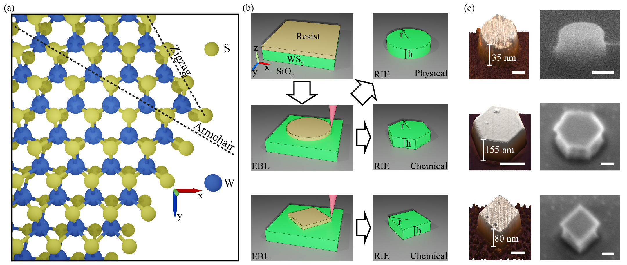
Fabrication of nano-antennas WS2 consists of covalently bonded monolayers (Fig. 1(a)) with a hexagonal crystal structure held together by van-der-Waals forces in bulk crystals. We mechanically exfoliated WS2 flakes onto a 290 nm SiO2 on silicon substrate with thicknesses ranging from 25 to 500 nm. Fig. 1(b) shows a schematic representation of the subsequent fabrication process. We spun a positive resist onto the sample and patterned circular disks and squares with varying radii using EBL. After development, we transferred the pattern into the WS2 crystals with RIE using two different recipes. Etching was terminated once the etch depth (estimated from the etching rate and time) matched the thickness of the exfoliated crystal, defining the nano-antenna height (see Methods). An anisotropic etch using a mixture of CHF3 and SF6 gases along with a high DC bias and low chamber pressure yielded circular nano-pillars with vertical sidewalls, which resulted from the physical etching of the resist pattern into the WS2. Examples of completed structures are shown in the AFM and scanning electron microscopy (SEM) images in the upper row of Fig. 1(c).
Upon substitution of the CHF3 with additional SF6 gas, a reduction of the DC bias and an increase in the chamber pressure, the resulting nano-antennas exhibited a hexagonal geometry with a radius defined from the center of the structure to one of the vertices at the edge, as shown in the middle right panel of Fig. 1(b). This definition corresponds to the radius of the previously circular resist pattern. The physical etching mechanism was suppressed and the increased proportion of reactive fluorine radicals ensured a dominant chemical etch, which preferentially removed the WS2 crystal in the armchair crystal axis leading to zigzag terminated sidewalls at 120∘ angles to each other following the crystal symmetry. This agrees with DFT results, which also predict that zigzag edges are more stable [46, 47]. The AFM and SEM images in the middle row of Fig. 1(c) display an example of hexagonal nano-antennas.
The final geometry we achieved was that of a square which resulted from a combination of resist patterning and chemical etching of the WS2. We defined a square resist pattern with sides oriented parallel to the zigzag axis of the crystal. The subsequent chemical etching similarly removed the WS2 in the armchair crystal axes ultimately leading to 90∘ angles describing a square shaped nano-antenna, examples of which are displayed in the lower panels of Fig. 1(c). The hexagonal geometry and, in part, the square nano-antenna geometry are formed due to the relative stability of the zigzag axis and can therefore lead to atomically sharp vertices.
Photonic resonances of WS2 nano-antennas We studied the fabricated structures using dark field spectroscopy and compared the experimental results to FDTD simulations, which yielded close agreement. We identified an electric dipole resonance with small contributions from higher order modes as well as anapole and higher order anapole modes (see Supplementary Note 1). As expected from Mie theory, the resonances forming in the studied nano-antennas red-shifted with increasing radius and blue-shifted with decreasing height. The ability to change the geometry of nano-antennas through a choice of etching recipe provides an additional, more precise tuning mechanism for the observed resonances (see Supplementary Note 2).
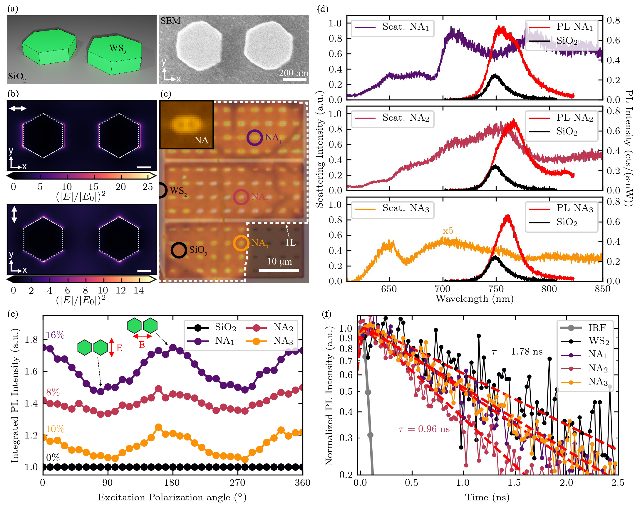
Next we considered more complex architectures by placing a pair of the novel hexagonal nano-pillars in close proximity to form a dimer nano-antenna shown schematically in the left panel of Fig. 2(a). An SEM image of a fabricated structure is also displayed in the right panel of Fig. 2(a). Dark field spectra of dimer nano-antennas also exhibit scattering Mie resonances as well as anapole modes which redshift with increasing size (see Supplementary Note 3). However, when two single nano-pillars are placed in close proximity to form a dimer, their photonic resonances hybridize forming two cross-polarized modes with an energy splitting (see Supplementary Note 4). One of these modes is excited with a polarization parallel to the axis connecting the midpoints of the single nano-pillars (dimer axis), which we name the X-pol mode, while the other is excited perpendicularly, here named the Y-pol mode. An intriguing result from this hybridization is the increased electric field intensity surrounding the side-walls of the nano-antennas. For the X-polarized mode, high electric field intensity hotspots form in the gap separating the two nano-pillars as shown in the upper panel of Fig. 2(b). For the Y-polarized mode, these hotspots form at the top and bottom wall of each nano-pillar as shown in the lower panel of Fig. 2(b). This confinement of the electric field intensity is expected to induce a large density of optical states suggesting that these nano-antennas are advantageous for Purcell enhancement of emission.
WSe2 monolayer photoluminescence enhancement In order to investigate whether these nano-structures can be used for such an application, we transferred a monolayer of WSe2 onto an array of WS2 dimer nano-antennas with a varying radius and gap distance using an all-dry technique (see Methods). A photoluminescence (PL) image of the completed sample is shown in Fig. 2(c). The brighter emission surrounding the nano-antenna sites is a first indication of the enhanced PL emitted by the monolayer due to an interaction with the dimer nano-antennas. The shape of this bright emission follows the outer walls of the nano-antennas, as seen in the inset of Fig. 2(c), similar to the calculated higher electric field intensity regions shown in Fig. 2(b).
In order to experimentally evaluate the photonic response of the structures, we subsequently measured the dark field spectra of three nano-antennas with a monolayer of WSe2 on top. These are displayed in Fig. 2(d) together with PL emission from the monolayer measured at each nano-antenna site. These structures have a height of 135 nm, a gap of 150 nm as well as a range of radii (NA1: r = 235 nm, NA2: r = 185 nm, NA3: r = 120 nm), representing an exemplary set of the measured nano-antennas from our sample, which included 86 dimers with nominal geometries corresponding to one of the three presented here. The overlap between the scattering Mie resonances and the PL spectrum suggests that all of the nano-structures may induce some emission enhancement; however, the strongest effect is expected from dimer NA2.
We subsequently carried out detailed room temperature photoluminescence measurements in a micro-PL setup in order to study the enhanced emission from the WSe2 monolayer in more detail. The excitation source, a pulsed laser (80 MHz) at 638 nm, was chosen to be below the WS2 absorption edge so that it would only be absorbed in the WSe2 monolayer and not in the nano-antennas. The spectra recorded at the position of the three dimer nano-antennas are displayed in Fig. 2(d) (red). These are compared to a PL spectrum measured from a flat portion of monolayer on SiO2 shown in black. The redshift of the PL spectrum observed here is due to strain in the monolayer as it conforms to the nano-antenna geometry [48]. This suggests that the WS2 dimer nano-antenna platform is ideal to study strain effects in monolayer TMDs similar to dimers fabricated from other dielectrics [48, 11]. The luminescence intensity from the monolayer at the nano-antenna positions is 3.5 to 4 times brighter. As the excitation spot is much larger than the nano-structures, we defined an experimental enhancement factor , similar to reference [7], in order to estimate the enhanced PL intensity:
| (1) |
where and are the spectrally integrated PL intensity measured on each dimer nano-antenna and on the flat SiO2 substrate respectively. The area of each dimer nano-antenna and the area of the laser spot are represented as and respectively. Using this definition, we calculated enhancement factors of 120, 235 and 241 for nano-antennas NA1, NA2 and NA3 respectively when compared to a flat monolayer on the SiO2 substrate. If monolayer emission from positions on bulk WS2 (seen at the left edge of Fig. 2(c)) rather than on flat SiO2 is used for comparison, the enhancement factors are estimated to be 246, 486 and 533 for nano-antennas NA1, NA2 and NA3 respectively. This is due to the lower monolayer PL on bulk WS2 when compared to flat SiO2, which we largely attribute to charge transfer between the WSe2 and WS2 crystal [49]. We also compared to simulations of the fluorescence intensity enhancement in the vicinity of dimer nano-antennas with the same geometry and found agreement (see Supplementary Note 5).
Another method of probing the photonic enhancement of the WSe2 emission due to the nano-antennas is to induce a linear polarization in the excitation source and rotate this with respect to the dimer axis. As the electric field intensity surrounding the nano-antennas is higher for the X-pol mode when compared to the Y-pol mode, which can be observed in Fig. 2(b), the PL intensity is also expected to increase for this polarization. In this experiment, the integrated intensity at each polarization angle was normalized to that from a monolayer region on flat SiO2, defined as , so as to highlight the effect of the nano-antenna photonic resonances. The results are shown in Fig. 2(e) where all structures yield a degree of linear polarization of the photoluminescence, shown on the left of each plot, confirming the coupling of the emission to the nano-antenna resonances.
The last experiment performed in order to study the photonic enhancement of WSe2 monolayer emission due to the WS2 dimer nano-antennas was a measurement of the PL decay time, displayed in Fig. 2(f). For this study, an avalanche photo-diode was used as a detector with an instrument response function (IRF, grey) defined by the laser pulse ( 90 ps). A very low excitation power density of 0.02 was used in order to avoid exciton-exciton annihilation processes, which dominate in these materials at higher powers [50]. The results yield single exponential decay lifetimes, which consist of contributions from both radiative and non-radiative recombination rates. An increase in the radiative rate due to photonic enhancement will lead to a decrease in the emission lifetime as this component is shortened. The intrinsic WSe2 monolayer PL lifetime at room temperature measured from the monolayer on the WS2 bulk crystal was ns. The PL decay times measured for NA1, NA2 and NA3 are ns, ns, ns respectively. These are lower than that measured on the bulk crystal suggesting the presence of Purcell enhancement. If we assume that the non-radiative rate contribution to the lifetime is low, we can extract Purcell factors of 1.33, 1.85 and 1.23 for NA1, NA2 and NA3 respectively. However, previous measurements of the quantum efficiency of WSe2 monolayers report values ranging from 0.06 to 5 [51, 52, 53], therefore, the non-radiative recombination rate is much higher than the radiative. As the Purcell factor only affects the radiative component of the lifetime, the values extracted above are only lower bounds on the emission enhancement factor, which may be much higher. As suggested by the higher overlap of the PL emission with the scattering resonances of the nano-antenna, the shortest PL lifetime was measured for NA2 where the highest Purcell enhancement is expected. This suggests that the enhancement factor can be modulated by tuning the dimer nano-antenna resonances closer or further from the PL emission energy of the monolayer (see Supplementary Note 5). We also varied the linear polarization of the excitation source and measured the PL decay time for the X-pol and Y-pol modes. For the majority of the measured nano-antenna sites, the X-pol mode yielded a lower lifetime than the Y-pol mode (see Supplementary Note 6) as expected from the higher simulated electric field intensities, in Fig. 2(b), and therefore higher Purcell factors.
As further evidence of the photonic capabilities of WS2 dimer nano-antennas, we performed second harmonic generation experiments using an anapole resonance present in 60 nm high nano-antennas with a radius of 205 nm and a gap of 130 nm. The anapole resonance at a wavelength of 800 nm led to confinement of the excitation laser and a 7.2 times enhanced SHG signal when compared with bulk crystal. The enhancement also proved to be polarization dependent in dimer nano-antennas, as opposed to monomers, as the electric fields are confined outside (inside) the nano-structure geometry for the X-pol (Y-pol) anapole mode. This behavior was confirmed by simulations of the confined electric energy, which also reveal that the SHG enhancement polarization orientation can be rotated with a change in excitation wavelength and its degree of linear polarization can be modulated with an increase in dimer gap (see Supplementary Note 7).
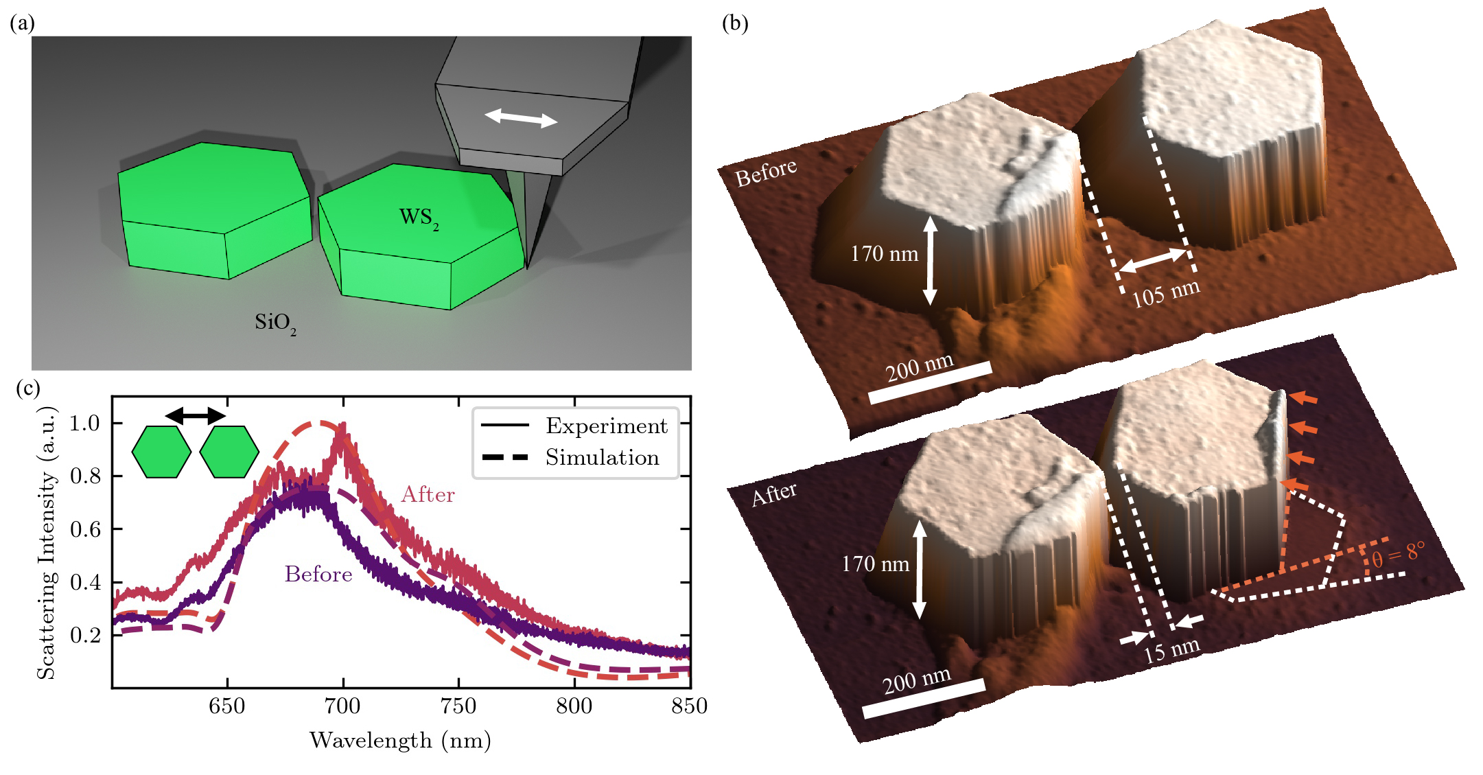
AFM repositioning The fabrication procedure outlined in Fig. 1 yields minimum dimer separation gaps of 50 nm, which result in resonances with limited electric field intensity and therefore Purcell factors. We attempted to improve upon this by using the properties of layered materials to our advantage. The relatively weak van-der-Waals forces, which facilitate mechanical exfoliation of thin WS2 crystals also allow for a weak adhesion of the fabricated structures to the SiO2/Si substrate. As a post-fabrication procedure, we employed an AFM cantilever in order to translate one nano-pillar with respect to the other and achieve gaps as small as 10 nm without damaging the nano-antenna. Smaller separation distances may be achievable; however, the accurate measurement of the gap width is a considerable challenge due to the finite size of the cantilever tip, which ranges from 1 to 10 nm.
Nano-antennas were repositioned by using AFM in contact mode. Scanning parallel to the dimer axis in a small area immediately adjacent to one nano-pillar with the scan slightly overlapping the distal edge of the nano-antenna forced the cantilever tip to displace the structure closer to the other. A schematic representation of the translation is shown in Fig. 3(a). Very fine positioning can be achieved using this method as shown in Fig. 3(b) where we translated one nano-pillar with respect to the other reducing the dimer gap separation from 105 nm to 155 nm.
An additional advantage of using this repositioning method is the ability to rotate the nano-pillars with great precision (<1∘). As shown in the bottom panel of Fig 3(b), by scanning the AFM cantilever along a tangent of one of the nano-pillars and contacting with only the edge, it was rotated by over 8∘. Scanning closer to the midpoint of the nano-pillar translated it closer to the other. These methods of contacting the AFM tip with the nano-pillars allow for fine positioning of the inside vertices of the dimer. The repositioning procedure is iterative and entirely reversible, allowing alignment to be fine-tuned or completely changed as necessary. Further AFM scans of repositioned nano-antennas are displayed in Supplementary Note 8 confirming the reproducibility of the procedure and showing the minimum gap separation we have achieved (105 nm).
To confirm that the AFM repositioning modified the photonic response, we performed dark field spectroscopy before and after the translation procedure. As shown in Fig. 3(c), the dipole resonance seen in scattering increased after repositioning for an excitation parallel to the dimer axis, which is the most sensitive configuration to changes in gap separation. The dashed curves in the same figure represent simulations of the geometry before and after repositioning with close agreement to experiment supporting the achievement of a 15 nm gap.
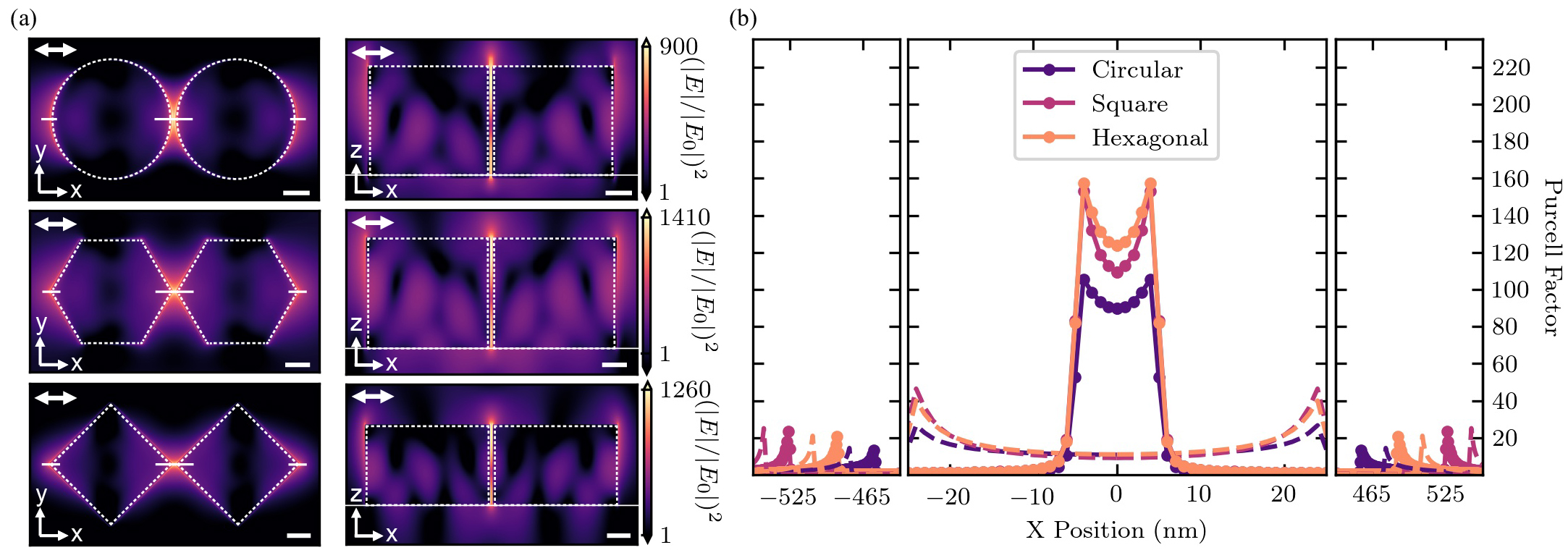
Electric field and Purcell enhancement of emission Ultra-small gaps, such as those achieved with the AFM repositioning technique, are expected to provide very high electric field confinements [39]. We therefore simulated the electric field intensity and Purcell enhancement induced by three dimer designs, corresponding to the different geometries shown in Fig. 1, with a gap of 10 nm. Each design was optimized for electric field confinement at the top surface of the dimer.
The electric field intensity spatial distribution is shown 0.5 nm above the top surface of the dimers in the left column of Fig. 4(a), and as a cross sectional cut along the z-axis through the middle of the individual nano-pillars in the right column of Fig. 4(a). Each distribution was calculated at the wavelength of the maximum electric field intensity (751.5 nm, 749.5 nm, 697.5 nm for the circular, hexagonal and square geometries respectively). The radii of the optimized geometries are r = 225 nm, r = 240 nm and r = 260 nm for the circular, hexagonal and square geometries respectively, while their heights are h = 200 nm, h = 200 nm and h = 150 nm. In order to closely approximate realistic structures, which can be fabricated, we measured the radius of curvature of the vertices of fabricated hexagonal and square dimer nano-antennas using atomic force microscopy. This yielded vertex radii of curvature as low as 22 nm for the hexagonal and 10 nm for the square geometry (see Supplementary Note 9). These values were then subsequently taken into account in the simulation of the hexagonal and square geometries. The electric field hotspots forming at the vertices between the two nano-pillars for an incident plane wave polarized parallel to the dimer axis exhibit intensities of more than 103 compared to vacuum as shown in Fig. 4(a). We compare the hotspots simulated for the three geometries achievable through the fabrication process. The hexagonal and square shaped nano-antennas induce a higher electric field intensity confinement than the circular design, with the hexagonal geometry inducing the largest enhancement.
Furthermore, we evaluated the Purcell factor for a single photon source positioned onto these structures by simulating a dipole emitter at positions along the dimer axis with a polarization parallel to the same axis. It is displaced by 0.5 nm from the top surface of the structure and its emission wavelength was set to the one used for the respective geometry in Fig. 4(a). The calculated Purcell factors at each position are shown in Fig. 4(b). Solid white lines in the left panels of Fig. 4(a) indicate the simulated positions of the emitter. The maxima seen at positions corresponding to the inner edges of the nano-antenna yield the largest results (>100) as expected from the electric field hotspots seen in Fig.4(a). Weakly confined hotspots at the outside edges of the structure also exhibit local maxima in the Purcell factor with values as high as 20. For the minimum achieved gap separation in the post-fabrication AFM repositioning, the hexagonal geometry exhibits the highest Purcell factor within its hotspot (157) with the square as a close second (153). The circularly shaped dimer leads to a maximal Purcell factor of 105. We have also simulated the Purcell factors for the minimum gap separation achievable without the use of AFM repositioning (50 nm), which are shown in Fig. 4(b) as dashed curves. This yields much smaller Purcell enhancements (as high as 46). There are several degrees of freedom in the fabrication process that can be used to modulate both the electric field intensity and the Purcell enhancements expected for these dimer structures. One method is to vary the gap separation of the dimer, leading to an exponential decrease in the electric field intensity and Purcell factor by one order of magnitude for a gap of 100 nm when compared to a gap of 10 nm. A similar decrease in both factors can also be achieved by rotation of one nano-pillar with respect to the other (see Supplementary Note 10). Such modulations can be experimentally achieved through the use of nano-fabrication techniques or AFM repositioning.
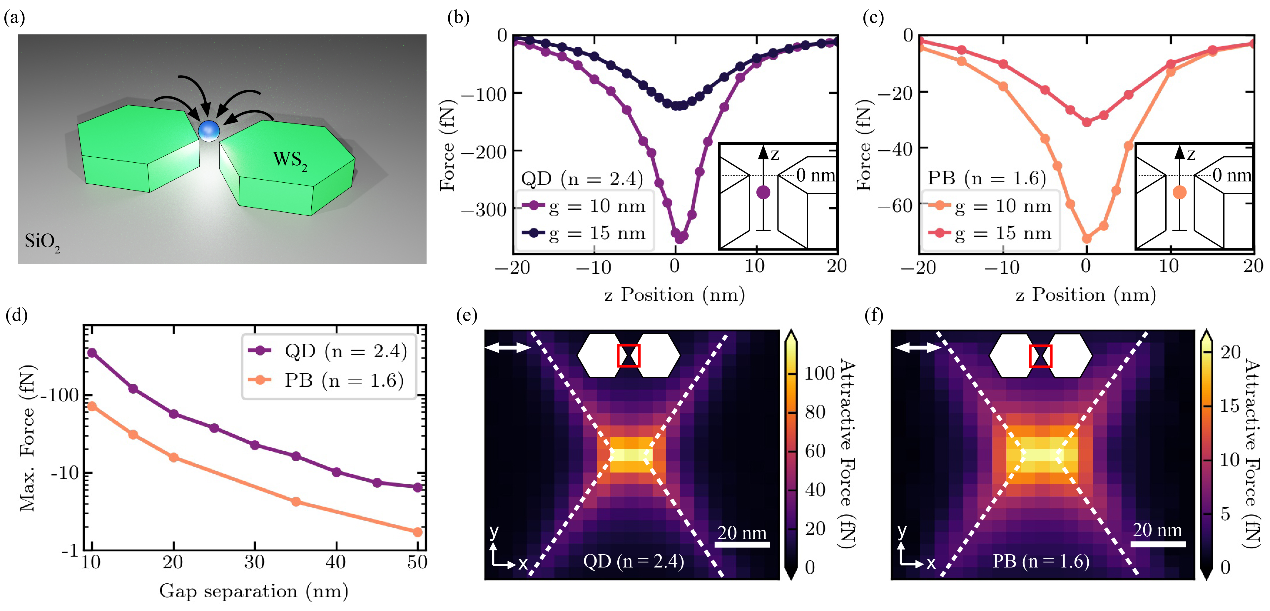
Dimer nano-antenna optical trapping In order to study the potential of ultra-small gap WS2 dimer nano-antennas for optical trapping, we perform numerical simulations based on the Finite Element Method (FEM) to determine the Maxwell Stress Tensor (MST) and calculate the force exerted on small dielectric particles. The simulation geometry consists of the earlier optimized hexagonal nano-antenna with the addition of a nano-sphere (r = 5 nm) with a refractive index corresponding to either an approximated colloidal quantum dot (n = 2.4) [44] or a polystyrene bead (n = 1.6), which closely mimics the refractive index and size of a large protein [54]. Since optical trapping experiments often require a suspension of the nano-particles in a solution, we set the background refractive index to that of water. For all simulations, we use an experimentally feasible pump power density of 10 . A schematic representation of the simulation is shown in Fig. 5(a).
We explore the optical force applied to the QD and the PB, shown in Fig. 5(b) and (c) respectively, as they are translated along the z-axis in the middle of the dimer gap. We simulate the forces for two gap separations of the dimer hexagonal nano-antenna (10 nm and 15 nm) and observe an attractive (negative) force, which is maximized at the top surface of the nano-antenna where the electric field hotspots are formed. We observe a maximum optical force of 353 fN on the QD and 73 fN on the PB for the dimer nano-antennas with a 10 nm separation. For the larger dimer gap (15 nm), this reduces to 123 fN on the QD and 31 fN on the PB. We also study the dependence of this maximum optical force in the electric field hotspots on the dimer gap, which is varied from 10 nm to 50 nm. As shown in Fig. 5(d), the maximum attractive force imparted on the nano-particles decreases exponentially by one order of magnitude as expected from the decay of the electric field intensity with an increased separation (see Supplementary Note 10).
We subsequently explore the lateral spatial dependence of the optical force by simulating the QD and PB in a plane, which is 5 nm above the top surface of the dimer nano-antenna with a 10 nm gap, as shown in Fig. 5(e) and (f). This is an emulation of the position of nano-particles placed onto the top surface of the dimer. The optical force, as expected, is maximized at the position of the electric field hotspots yet still maintains values of more than 100 fN for the QD and 20 fN for the PB.
Discussion
We have fabricated and characterized both monomer and dimer WS2 nano-antennas with the aim to highlight the advantages of their use in photonic applications such as tunable photoluminescence enhancement, polarization dependent SHG enhancement, SPE enhancement and optical trapping thereby broadening the versatility of TMD nano-antennas. Dark field studies on monomer and dimer nano-antennas reveal a straightforward approach for tuning resonances in the structures in order to fit with different applications by varying the radius, height or geometry. We couple monolayer WSe2 emission to the dimer resonances in the same, TMD, material system and achieve PL enhancement factors of more than 240 and a Purcell enhancement factor lower bound of nearly 2. Through the use of a dimer anapole mode we show polarization dependent SHG enhancement, not present in bulk TMD flakes or monomer nano-antennas, that can be rotated by a change in excitation polarization which may provide advantageous for the realization of optical logic gates [55]. Post-fabrication repositioning of dimer nano-antennas utilizing AFM led us to attain ultra-small gaps of 105 nm, on the order of the feature resolution limit set by FIB milling [56], which we achieve through a more precise, less damaging technique. Although a previous report has demonstrated AFM positioning of plasmonic bowtie nano-antennas [57], this technique has only become possible for dielectric nano-antennas made from layered materials due to their intrinsic van-der-Waals attractive forces. This allows us to achieve the smallest separation recorded for a dielectric resonator defined through the use of electron beam lithography followed by reactive ion etching[58, 25]. Another advantage of this method is the possibility to change the relative orientation of individual nano-pillars, thereby, aligning their potentially atomically sharp vertices in closer or further proximity.
The numerical simulation studies of dimer nano-antennas exhibiting an ultra-small gap yield highly confined electric field intensity hotspots (103 enhancement compared to vacuum). We predict the practical utility of WS2 nano-antennas for radiative rate enhancement of single photon emission with Purcell factors of up to 157 for a hexagonal and 153 for a square geometry. The expected quantum emission enhancement in the dimer nano-antennas is higher than the largest currently achieved in photonic crystal cavities [59] due to the previously inaccessibly small proximity attained with the AFM repositioning method. We also explore two different routes to modulate the photonic enhancement through variation of the dimer gap as well as the relative rotation of the individual nano-pillars, which are both controllable either through the fabrication process or, to a greater precision, the post-fabrication repositioning. These methods of controlling the emission properties of single photon sources may prove useful for WSe2 SPEs, which form at high strain gradients in monolayers transferred onto dimer nano-antennas collocated with the electric field hotspots [48]. Previous reports have shown quantum efficiency enhancement for WSe2 SPEs [11] as well as rotation of the emitter dipole moment due to a change in the strain gradient [60] both of which can be controlled by a change in separation and rotation of individual nano-pillars in the dimer nano-antenna through AFM repositioning.
We further explored a route to the precise positioning of SPEs by simulating optical trapping forces due to the highly confined electric field in the gap of the dimer nano-antennas. We calculated a maximum attractive force of 353 fN for a colloidal quantum dot and 73 fN for a protein-like, polystyrene bead both with a radius of 5 nm under a pump power density of 10 . When compared to previous examples of dielectric nano-antennas for optical trapping, the WS2 dimers yield higher attractive forces by a factor of >83 for QDs [44] and >40 for PBs [25] with the same size and under the same pump power conditions. Therefore, WS2 dimer nano-antennas with ultra-small gaps show great potential for applications of stable trapping of very small nano-particles with a moderate optical power. This once again highlights the advantage of the AFM repositioning technique to reduce the dimer gap below the limits available to standard nano-fabrication. The large Purcell enhancements and optical trapping forces predicted for WS2 dimer nano-antennas with ultra-small gaps highlight the unique potential for TMD nano-resonator research and applications. This is possible due to the refractive index and van-der-Waals forces, which allow the formation of highly confined resonances and hotspots while simultaneously opening the possibility of AFM repositioning. The field of nano-photonics includes a diverse library of materials and here we assert and expand the possibilities provided by adding thin crystals of TMDs to the list.
Methods
Sample fabrication
WS2 exfoliation: WS2 flakes were mechanically exfoliated from bulk crystal (HQ-graphene) onto a nominally 290 nm SiO2 on silicon substrate. Large flakes with recognizable crystal axes via straight edged sides at 120∘ to each other were identified and their positions within the sample were recorded for further patterning.
Electron beam lithography: Samples were spin coated with ARP-9 resist (AllResist GmbH) at 3500 rpm for 60 s and baked at 180∘ for 5 min yielding a film of 200 nm thickness. Electron beam lithography was performed in a Raith GmbH Voyager system operating at 50 kV using a beam current of 560 pA.
Reactive ion etching: Anisotropic etching to imprint the resist pattern into the WS2 flakes physically was carried out using a mixture of CHF3 (14.5 sccm) and SF6 (12.5 sccm) at a DC bias of 180 V and a pressure of 0.039 mbar for 40 seconds. Isotropic etching was achieved by using a more chemical recipe with solely SF6 (20 sccm) at a DC bias of 50 V and a pressure of 0.13 mbar for 40 seconds. Removal of the remaining resist after etching was accomplished by a bath in warm 1165 resist remover (1 hour) followed by Acetone (5 min) and IPA (5 min). If resist is still found on the sample, final cleaning is done in a bath of Acetone (1 hour) and IPA (5 min) followed by 1 hour in a UV ozone treatment. In some cases, the structures were slightly overetched leading to nano-antennas with a small pedestal of SiO2 (<20 nm). This, however, did not lead to any noticeable changes in the photonic resonances nor in the ability to reposition the structures with AFM.
WSe2 transfer: WSe2 monolayers were mechanically exfoliated from a bulk crystal (HQ-graphene) onto a (PDMS) stamp, which had previously been attached to a glass slide. Large monolayers were identified using PL imaging. The glass slide is rotated upside down and attached to a holder arm by means of a vacuum. The target substrate, consisting of WS2 nano-antennas on a SiO2 surface, was also held to a stage using the same vacuum. The WSe2 monolayer was slowly brought into contact with the target substrate through the use of a piezo-scanner stage. After the entire monolayer has contacted the surface, the glass slide with PDMS was slowly moved away from the target substrate. The low speed of the peeling process makes use of the visco-elastic properties of the PDMS polymer and leaves the monolayer of WSe2 onto the substrate.
Dark field spectroscopy
Optical spectroscopy in a dark field configuration was achieved using a Nikon LV150N microscope with a fiber-coupled output. Incident illumination from a tungsten halogen lamp in the microscope was guided to a circular beam block with a diameter smaller than the beam diameter. The light was then reflected by a 50:50 beam-splitter towards a 50x Nikon (0.8 NA) dark-field objective which only illuminates the sample at large angles to the normal. Reflected light from the sample is guided back through the same objective towards a fiber coupler. Due to the small diameter of the multi-mode fiber core used, only light reflected back at small angles to the normal is collected. The fiber from the microscope was subsequently coupled to a Princeton Instruments spectrometer and charge coupled device (CCD).
Micro-Photoluminescence spectroscopy
In order to record the photoluminescence emitted from monolayer WSe2 at different regions of our sample, we used a home-built setup, which includes a pulsed diode laser at 638 nm. The sample was mounted into an Oxford Instruments flow cryostat and the chamber was pumped to vacuum. The collimated excitation laser was passed through a 700 nm short-pass filter, a Glan-Thompson linear polarizer and a half wave plate before being deflected by a 50:50 beam-splitter and passing through a 100x (0.7 NA) Mitutoyo objective which focused the beam onto the sample. The emitted light is collected by the same objective and passes through the beam-splitter to be guided through a 700 nm long-pass filter and is focused onto the slit of a Princeton Instruments spectrometer (0.75 meter) and CCD (data shown in Figs. 2(d) and (e) and Supplementary Note 5 and 6). The PL decay time studies utilized the pulsed laser excitation and the emitted light was spectrally filtered (10 nm) using the exit slit of the spectrometer before it was fiber-coupled to an ID Quantique avalanche photo-diode (id100) (data shown in Fig. 2(f) and Supplementary Note 6).
Atomic force microscope repositioning and imaging
All repositioning was carried out using a JPK Nanowizard 3 Ultra AFM using Bruker SNL probes (cantilever C, nominal stiffness 0.24 N/m). First, nano-antennas were imaged in QI mode with a setpoint of 1 nN, a Z length of 400 nm and a pixel time of 15 ms. To reposition the nano-antennas, the AFM was switched to contact mode and 200 nm scans were performed with a setpoint of 1 nN and a scan rate of 2 Hz on the substrate immediately adjacent to the nano-antenna. The fast scan axis was oriented along the desired direction of movement and the scan area was progressively moved so that the scan overlapped with the nano-antenna to translate it in the desired direction in increments of 5-50 nm at a time. Periodically, the nano-antenna was re-imaged in QI mode to check the relative position and orientation of the pillars. Final characterization after repositioning was performed in QI mode.
FDTD simulations The finite-difference time-domain simulations were carried out using Lumerical Inc. software.
Scattering simulations: Calculations of the scattering cross section shown in Fig. 3 and Supplementary Notes 1 and 3 were carried out by defining the geometry of the WS2 nano-antennas onto a SiO2 substrate utilizing the refractive index of WS2 from reference [20]. Illumination with a plane wave was sent normal to the surface using a TFSF source from the air side. The illumination was unpolarized, however, for Fig. 3 the polarization was set parallel to the dimer axis. The scattered intensity was subsequently collected from a monitor set above the illumination plane (in the far-field) so that the dark field spectroscopy experiments could be closely emulated.
Electric field intensity simulations: Calculations of the near-field electric field intensity normalized to vacuum, shown in Figs. 2(b) and 4(a) were simulated using the same geometry and illumination scheme as for the scattering simulations (polarization is shown as a white double arrow in top left corner of each panel) with a monitor recording the electric field 0.5 nm above the top surface of the nano-antennas or as a vertical cross-section of the structure passing through the dimer axis as shown in the right-most panels of Fig. 4(a). For Supplementary Note 7, the monitor was designed as a cross-sectional profile through the midpoint of the nano-antenna height. For Figs. 2(b) and 4(a) this monitor was defined to encompass the entire cross section of the nano-antennas. For the simulations performed in Supplementary Note 5 and 10, only a single point 1 nm from the inside edge of the dimer nano-antenna within the hotspot was recorded.
Purcell factor simulations: Simulations of the Purcell factor were carried out using the same geometry as for the electric field intensity simulations. The illumination was achieved through a dipole source placed at different positions, 0.5 nm above the top surface of the nano-antenna with a polarization parallel to the dimer axis for Fig. 4(b). For the simulations carried out in Supplementary Note 6, the polarization was set parallel and perpendicular to the dimer axis in order to compare the two. For the simulations displayed in Supplementary Note 10 however, the position was set to 0.5 nm above the top surface of the nano-antenna and 1 nm away from the inside edge within the electric field hotspot.
Optical trapping force simulations: We have used the 3D finite element method (COMSOL Multiphysics) to calculate the optical forces in the hexagonal dimer nano-antenna. The structure is illuminated with a plane wave propagating in a normal direction to the top surface of the structure with a polarization along the dimer axis. The background refractive index was set to that of water to enable access of the bead to the trapping site. We have calculated the optical forces at the resonance of the nano-antenna, corresponding to the maximum energy enhancement. The value of the optical force is obtained by integrating the Maxwell Stress Tensor on the surface of the target nano-particle [41]. A fine mesh (resolution of 3 nm) has been employed in the dimer gap to calculate the electromagnetic distribution with a high accuracy, minimizing the error on the evaluation of the optical force. The computational domain has been set to a sufficiently large value (>2 ) and surrounded by perfectly matched layers in order to avoid undesired reflection and scattering from the boundary.
Acknowledgments
P. G. Z., L. S., T.S.M., M.S., A. G. and A. I. T. thank the financial support of the European Graphene Flagship Project under grant agreements 881603 and EPSRC grants EP/S030751/1, EP/V006975/1 and EP/P026850/1. L. S. and A. I. T. thank the European Union’s Horizon 2020 research and innovation programme under ITN Spin-NANO Marie Sklodowska-Curie grant agreement no. 676108. P. G. Z. and A. I. T. thank the European Union’s Horizon 2020 research and innovation programme under ITN 4PHOTON Marie Sklodowska-Curie grant agreement no. 721394. T.F.K. acknowledges the support of the Engineering and Physical Sciences Research Council (grant number EP/P030017/1). Y.W. acknowledges a Research Fellowship (TOAST) awarded by the Royal Academy of Engineering. We would also like to thank Cynthia Vidal for her contribution to the photoluminescence measurements of monolayer WSe2 on WS2 dimer nano-antennas.
Author contributions
P.G.Z and L.S. exfoliated WS2 layers onto SiO2 substrates. Y.W. fabricated nano-antenna structures using EBL and RIE. P.G.Z and Y.W. performed AFM and SEM characterization of fabricated nano-antennas. P.G.Z. carried out dark field spectroscopy measurements, micro-PL measurements, scattering cross section simulations and electric/magnetic field intensity profile simulations for identification of WS2 nano-antenna resonances. P.G.Z., T.S.M. and A.G. performed second harmonic generation experiments on WS2 nano-antennas. N.M. repositioned dimer nano-antennas using AFM. P.G.Z. and M.S., simulated electric field intensity profiles and Purcell factors for optimized dimer nano-antennas as well as for studies on dimer gap separation and rotation. D.C. performed optical trapping simulations and analyzed the results with Y.W., T.F.K. P.G.Z., L.S., T.S.M. and A.I.T. analyzed various optical spectroscopy data. J.H., T.F.K., Y.W. and A.I.T. managed various aspects of the project. P.G.Z. and A.I.T. wrote the manuscript with contributions from all co-authors. P.G.Z., L.S., Y.W., N.M., D.C., J.H., A.I.T. and T.F.K. conceived the experiments and simulations. A.I.T. oversaw the entire project.
References
- [1] Kin Fai Mak, Changgu Lee, James Hone, Jie Shan, and Tony F. Heinz. Atomically thin MoS2: A new direct-gap semiconductor. Physical Review Letters, 105(13):136805, 2010.
- [2] Gang Wang, Alexey Chernikov, Mikhail M. Glazov, Tony F. Heinz, Xavier Marie, Thierry Amand, and Bernhard Urbaszek. Colloquium: Excitons in atomically thin transition metal dichalcogenides. Reviews of Modern Physics, 90(2):21001, 2018.
- [3] Fengnian Xia, Han Wang, Di Xiao, Madan Dubey, and Ashwin Ramasubramaniam. Two-dimensional material nanophotonics. Nature Photonics, 8:899–907, 2014.
- [4] S. Dufferwiel, T. P. Lyons, D. D. Solnyshkov, A. A. P. Trichet, F. Withers, G. Malpuech, J. M. Smith, K. S. Novoselov, M. S. Skolnick, D. N. Krizhanovskii, and A. I. Tartakovskii. Valley coherent exciton-polaritons in a monolayer semiconductor. Nature Communications, 9:4797, 2018.
- [5] Long Zhang, Rahul Gogna, Will Burg, Emanuel Tutuc, and Hui Deng. Photonic-crystal exciton-polaritons in monolayer semiconductors. Nature Communications, 9:713, 2018.
- [6] Alex Krasnok, Sergey Lepeshov, and Andrea Alú. Nanophotonics with 2D transition metal dichalcogenides. Optics Express, 26(12):15972–15994, 2018.
- [7] L. Sortino, P. G. Zotev, S. Mignuzzi, J. Cambiasso, D. Schmidt, A. Genco, M. Aßmann, M. Bayer, S. A. Maier, R. Sapienza, and A. I. Tartakovskii. Enhanced light-matter interaction in an atomically thin semiconductor coupled with dielectric nano-antennas. Nature Communications, 10:5119, 2019.
- [8] Sanfeng Wu, Sonia Buckley, John R. Schaibley, Liefeng Feng, Jiaqiang Yan, David G. Mandrus, Fariba Hatami, Wang Yao, Jelena Vučković, Arka Majumdar, and Xiaodong Xu. Monolayer semiconductor nanocavity lasers with ultralow thresholds. Nature, 520:69–72, 2015.
- [9] Tao Cai, Je Hyung Kim, Zhili Yang, Subhojit Dutta, Shahriar Aghaeimeibodi, and Edo Waks. Radiative Enhancement of Single Quantum Emitters in WSe2 Monolayers Using Site-Controlled Metallic Nanopillars. ACS Photonics, 5(9):3466–3471, 2018.
- [10] Yue Luo, Gabriella D. Shepard, Jenny V. Ardelean, Daniel A. Rhodes, Bumho Kim, Katayun Barmak, James C. Hone, and Stefan Strauf. Deterministic coupling of site-controlled quantum emitters in monolayer WSe2 to plasmonic nanocavities. Nature Nanotechnology, 13:1137–1142, 2018.
- [11] Luca Sortino, Panaiot G. Zotev, Catherine L. Phillips, Alistair J. Brash, Javier Cambiasso, Elena Marensi, A. Mark Fox, Stefan A. Maier, Riccardo Sapienza, and Alexander I. Tartakovskii. Bright single photon emitters with enhanced quantum efficiency in a two-dimensional semiconductor coupled with dielectric nano-antennas. Nature Communications, 12:6063, 2021.
- [12] Nils Bernhardt, Kirill Koshelev, Simon J.U. White, Kelvin Wong Choon Meng, Johannes E. Fröch, Sejeong Kim, Toan Trong Tran, Duk-Yong Yong Choi, Yuri Kivshar, and Alexander S. Solntsev. Quasi-BIC Resonant Enhancement of Second-Harmonic Generation in WS2 Monolayers. Nano Letters, 20(7):5309–5314, 2020.
- [13] Vasily Kravtsov, Ekaterina Khestanova, Fedor A. Benimetskiy, Tatiana Ivanova, Anton K. Samusev, Ivan S. Sinev, Dmitry Pidgayko, Alexey M. Mozharov, Ivan S. Mukhin, Maksim S. Lozhkin, Yuri V. Kapitonov, Andrey S. Brichkin, Vladimir D. Kulakovskii, Ivan A. Shelykh, Alexander I. Tartakovskii, Paul M. Walker, Maurice S. Skolnick, Dmitry N. Krizhanovskii, and Ivan V. Iorsh. Nonlinear polaritons in a monolayer semiconductor coupled to optical bound states in the continuum. Light: Science and Applications, 9:56, 2020.
- [14] Kin Fai Mak and Jie Shan. Photonics and optoelectronics of 2D semiconductor transition metal dichalcogenides. Nature Photonics, 10:216–226, 2016.
- [15] Sejeong Kim, Johannes E. Fröch, Joe Christian, Marcus Straw, James Bishop, Daniel Totonjian, Kenji Watanabe, Takashi Taniguchi, Milos Toth, and Igor Aharonovich. Photonic crystal cavities from hexagonal boron nitride. Nature Communications, 9:2623, 2018.
- [16] Johannes E. Fröch, Yongsop Hwang, Sejeong Kim, Igor Aharonovich, and Milos Toth. Photonic Nanostructures from Hexagonal Boron Nitride. Advanced Optical Materials, 7:1801344, 2019.
- [17] H. H. Fang, B. Han, C. Robert, M. A. Semina, D. Lagarde, E. Courtade, T. Taniguchi, K. Watanabe, T. Amand, B. Urbaszek, M. M. Glazov, and X. Marie. Control of the Exciton Radiative Lifetime in van der Waals Heterostructures. Physical Review Letters, 123(6):067401, 2019.
- [18] Kaiyuan Yao, Nathan R. Finney, Jin Zhang, Samuel L. Moore, Lede Xian, Nicolas Tancogne-Dejean, Fang Liu, Jenny Ardelean, Xinyi Xu, Dorri Halbertal, K. Watanabe, T. Taniguchi, Hector Ochoa, Ana Asenjo-Garcia, Xiaoyang Zhu, D. N. Basov, Angel Rubio, Cory R. Dean, James Hone, and P. James Schuck. Enhanced tunable second harmonic generation from twistable interfaces and vertical superlattices in boron nitride homostructures. Science Advances, 7(10):1–8, 2021.
- [19] Rebeca Ribeiro-Palau, Changjian Zhang, Kenji Watanabe, Takashi Taniguchi, James Hone, and Cory R. Dean. Twistable electronics with dynamically rotatable heterostructures. Science, 361(6403):690–693, 2018.
- [20] Ruggero Verre, Denis G. Baranov, Battulga Munkhbat, Jorge Cuadra, Mikael Käll, and Timur Shegai. Transition metal dichalcogenide nanodisks as high-index dielectric Mie nanoresonators. Nature Nanotechnology, 14:679–683, 2019.
- [21] Yoonhyuk Rah, Yeonghoon Jin, Sejeong Kim, and Kyoungsik Yu. Optical analysis of the refractive index and birefringence of hexagonal boron nitride from the visible to near-infrared. Optics Letters, 44:3797–3800, 2019.
- [22] Javier Cambiasso, Gustavo Grinblat, Yi Li, Aliaksandra Rakovich, Emiliano Cortés, and Stefan A. Maier. Bridging the Gap between Dielectric Nanophotonics and the Visible Regime with Effectively Lossless Gallium Phosphide Antennas. Nano Letters, 17(2):1219–1225, 2017.
- [23] Reuben M. Bakker, Dmitry Permyakov, Ye Feng Yu, Dmitry Markovich, Ramón Paniagua-Domínguez, Leonard Gonzaga, Anton Samusev, Yuri Kivshar, Boris Lukyanchuk, and Arseniy I. Kuznetsov. Magnetic and electric hotspots with silicon nanodimers. Nano Letters, 15(3):2137–2142, 2015.
- [24] Javier Cambiasso, Matthias König, Emiliano Cortés, Sebastian Schlücker, and Stefan A. Maier. Surface-Enhanced Spectroscopies of a Molecular Monolayer in an All-Dielectric Nanoantenna. ACS Photonics, 5(4):1546–1557, 2018.
- [25] Zhe Xu, Wuzhou Song, and Kenneth B. Crozier. Optical Trapping of Nanoparticles Using All-Silicon Nanoantennas. ACS Photonics, 5(12):4993–5001, 2018.
- [26] Yilei Li, Alexey Chernikov, Xian Zhang, Albert Rigosi, Heather M Hill, Arend M Van Der Zande, Daniel A Chenet, En-min Shih, James Hone, and Tony F Heinz. Measurement of the optical dielectric function of monolayer transition-metal dichalcogenides : MoS2, MoSe2, WS2, and WSe2. Physical Review B, 90:205422, 2014.
- [27] G. A. Ermolaev, D. V. Grudinin, Y. V. Stebunov, V. G. Kravets, J. Duan, G. I. Tselikov, K. V. Voronin, D. I. Yakubovsky, S. M. Novikov, D. G. Baranov, A. Y. Nikitin, T. Shegai, P. Alonso-González, A. N. Grigorenko, A. V. Arsenin, K. S. Novoselov, and V. S. Volkov. Giant optical anisotropy in transition metal dichalcogenides for next-generation photonics. Nature Communications, 12:854, 2021.
- [28] Riccardo Frisenda, Efrén Navarro-Moratalla, Patricia Gant, David Pérez De Lara, Pablo Jarillo-Herrero, Roman V. Gorbachev, and Andres Castellanos-Gomez. Recent progress in the assembly of nanodevices and van der Waals heterostructures by deterministic placement of 2D materials. Chemical Society Reviews, 47:53–68, 2018.
- [29] M. M. Benameur, B. Radisavljevic, J. S. Héron, S. Sahoo, H. Berger, and A. Kis. Visibility of dichalcogenide nanolayers. Nanotechnology, 22:125706, 2011.
- [30] Xingwang Zhang, Xiaojie Zhang, Wenzhuo Huang, Kedi Wu, Mengqiang Zhao, A. T. Charlie Johnson, Sefaattin Tongay, and Ertugrul Cubukcu. Ultrathin WS2-on-Glass Photonic Crystal for Self-Resonant Exciton-Polaritonics. Advanced Optical Materials, 8:1901988, 2020.
- [31] Huiqin Zhang, Bhaskar Abhiraman, Qing Zhang, Jinshui Miao, Kiyoung Jo, Stefano Roccasecca, Mark W. Knight, Artur R. Davoyan, and Deep Jariwala. Hybrid exciton-plasmon-polaritons in van der Waals semiconductor gratings. Nature Communications, 11:3552, 2020.
- [32] Battulga Munkhbat, Denis G. Baranov, Michael Stührenberg, Martin Wersäll, Ankit Bisht, and Timur Shegai. Self-Hybridized Exciton-Polaritons in Multilayers of Transition Metal Dichalcogenides for Efficient Light Absorption. ACS Photonics, 6(1):139–147, 2019.
- [33] Xingwang Zhang, Chawina De-Eknamkul, Jie Gu, Alexandra L. Boehmke, Vinod M. Menon, Jacob Khurgin, and Ertugrul Cubukcu. Guiding of visible photons at the ångström thickness limit. Nature Nanotechnology, 14:844–850, 2019.
- [34] Sebastian Busschaert, Moritz Cavigelli, Ronja Khelifa, Achint Jain, and Lukas Novotny. TMDC Resonators for Second Harmonic Signal Enhancement. ACS Photonics, 7(9):2482–2488, 2020.
- [35] Thomas D. Green, Denis G. Baranov, Battulga Munkhbat, Ruggero Verre, Timur Shegai, and Mikael Käll. Optical material anisotropy in high-index transition metal dichalcogenide Mie nanoresonators. Optica, 7:680–686, 2020.
- [36] Haonan Ling, Renjie Li, and Artur R. Davoyan. All van der Waals Integrated Nanophotonics with Bulk Transition Metal Dichalcogenides. ACS Photonics, 8(3):721–730, 2021.
- [37] Naseer Muhammad, Yang Chen, Cheng Wei Qiu, and Guo Ping Wang. Optical Bound States in Continuum in MoS2-Based Metasurface for Directional Light Emission. Nano Letters, 21(2):967–972, 2021.
- [38] Hasan Ahmed and Viktoriia E. Babicheva. Resonant and scattering properties of tungsten disulfide WS2 nanoantennas. Proceedings of SPIE, 11289R, 2020.
- [39] Hyeongrak Choi, Mikkel Heuck, and Dirk Englund. Self-Similar Nanocavity Design with Ultrasmall Mode Volume for Single-Photon Nonlinearities. Physical Review Letters, 118:223605, 2017.
- [40] Anika Kinkhabwala, Zongfu Yu, Shanhui Fan, Yuri Avlasevich, Klaus Müllen, and W. E. Moerner. Large single-molecule fluorescence enhancements produced by a bowtie nanoantenna. Nature Photonics, 3:654–657, 2009.
- [41] Donato Conteduca, Christopher Reardon, Mark G. Scullion, Francesco Dell’Olio, Mario N. Armenise, Thomas F. Krauss, and Caterina Ciminelli. Ultra-high Q/V hybrid cavity for strong light-matter interaction. APL Photonics, 2:086101, 2017.
- [42] Kai Wang, Ethan Schonbrun, Paul Steinvurzel, and Kenneth B. Crozier. Trapping and rotating nanoparticles using a plasmonic nano-tweezer with an integrated heat sink. Nature Communications, 2:469, 2011.
- [43] Russell A. Jensen, I. Chun Huang, Ou Chen, Jennifer T. Choy, Thomas S. Bischof, Marko Lončar, and Moungi G. Bawendi. Optical Trapping and Two-Photon Excitation of Colloidal Quantum Dots Using Bowtie Apertures. ACS Photonics, 3(3):423–427, 2016.
- [44] Zhe Xu and Kenneth B. Crozier. All-dielectric nanotweezers for trapping and observation of a single quantum dot. Optics Express, 27:4034–4045, 2019.
- [45] Battulga Munkhbat, Andrew B Yankovich, Denis G. Baranov, Ruggero Verre, Eva Olsson, and Shegai Timur. Transition metal dichalcogenide metamaterials with atomic precision. Nature Communications, 11:4604, 2020.
- [46] Yafei Li, Zhen Zhou, Shengbai Zhang, and Zhongfang Chen. MoS2 Nanoribbons : High Stability and Unusual Electronic and Magnetic Properties. Journal of the American Chemical Society, 130(49):16739–16744, 2008.
- [47] Shao-long Xiao, Wen-zhe Yu, and Shang-peng Gao. Surface Science Edge preference and band gap characters of MoS2 and WS2 nanoribbons. Surface Science, 653:107–112, 2016.
- [48] Luca Sortino, Matthew Brooks, Panaiot G. Zotev, Armando Genco, Javier Cambiasso, Sandro Mignuzzi, Stefan A. Maier, Guido Burkard, Riccardo Sapienza, and Alexander I. Tartakovskii. Dielectric nano-antennas for strain engineering in atomically thin two-dimensional semiconductors. ACS Photonics, 7(9):2413–2422, 2020.
- [49] Seunghyun Lee and Zhaohui Zhong. Nanoelectronic circuits based on two-dimensional atomic layer crystals. Nanoscale, 6(22):13283–13300, 2014.
- [50] Shinichiro Mouri, Yuhei Miyauchi, Minglin Toh, Weijie Zhao, Goki Eda, and Kazunari Matsuda. Nonlinear photoluminescence in atomically thin layered WSe2 arising from diffusion-assisted exciton-exciton annihilation. Physical Review B - Condensed Matter and Materials Physics, 90(15):1–5, 2014.
- [51] Nur Baizura Mohamed, Feijiu Wang, Hong En Lim, Wenjin Zhang, Sandhaya Koirala, Shinichiro Mouri, Yuhei Miyauchi, and Kazunari Matsuda. Evaluation of photoluminescence quantum yield of monolayer WSe2 using reference dye of 3-borylbithiophene derivative. Physica Status Solidi (B) Basic Research, 254(2), 2017.
- [52] Hyungjin Kim, Geun Ho Ahn, Joy Cho, Matin Amani, James P. Mastandrea, Catherine K. Groschner, Der Hsien Lien, Yingbo Zhao, Joel W. Ager, Mary C. Scott, Daryl C. Chrzan, and Ali Javey. Synthetic WSe2 monolayers with high photoluminescence quantum yield. Science Advances, 5(1), 2019.
- [53] Shrawan Roy, Anir S. Sharbirin, Yongjun Lee, Won Bin Kim, Tae Soo Kim, Kiwon Cho, Kibum Kang, Hyun Suk Jung, and Jeongyong Kim. Measurement of quantum yields of monolayer tmds using dye-dispersed pmma thin films. Nanomaterials, 10(6), 2020.
- [54] Gavin Young, Nikolas Hundt, Daniel Cole, Adam Fineberg, Joanna Andrecka, Andrew Tyler, Anna Olerinyova, Ayla Ansari, Erik G. Marklund, Miranda P. Collier, Shane A. Chandler, Olga Tkachenko, Joel Allen, Max Crispin, Neil Billington, Yasuharu Takagi, James R. Sellers, Cedric Eichmann, Philip Selenko, Lukas Frey, Roland Riek, Martin R. Galpin, Weston B. Struwe, Justin L.P. Benesch, and Philipp Kukura. Quantitative mass imaging of single molecules in solution. Science, 360(6387):423–427, 2017.
- [55] F. A. Bovino, M. Giardina, M. C. Larciprete, A. Belardini, M. Centini, C. Sibilia, M. Bertolotti, A. Passaseo, and V. Tasco. Optical logic functions with nonlinear gallium nitride nanoslab. Optics Express, 17(22):19337–19344, 2009.
- [56] Lukas Novotny and Niek Van Hulst. Antennas for light. Nature Photonics, 5:83–90, 2011.
- [57] Jörg Merlein, Matthias Kahl, Annika Zuschlag, Alexander Sell, Andreas Halm, Johannes Boneberg, Paul Leiderer, Alfred Leitenstorfer, and Rudolf Bratschitsch. Nanomechanical control of an optical antenna. Nature Photonics, 2:230–233, 2008.
- [58] Raju Regmi, Johann Berthelot, Pamina M. Winkler, Mathieu Mivelle, Julien Proust, Frédéric Bedu, Igor Ozerov, Thomas Begou, Julien Lumeau, Hervé Rigneault, María F. García-Parajó, Sébastien Bidault, Jérôme Wenger, and Nicolas Bonod. All-Dielectric Silicon Nanogap Antennas to Enhance the Fluorescence of Single Molecules. Nano Letters, 16(8):5143–5151, 2016.
- [59] Feng Liu, Alistair J. Brash, John O’Hara, Luis M.P.P. Martins, Catherine L. Phillips, Rikki J. Coles, Benjamin Royall, Edmund Clarke, Christopher Bentham, Nikola Prtljaga, Igor E. Itskevich, Luke R. Wilson, Maurice S. Skolnick, and A. Mark Fox. High Purcell factor generation of indistinguishable on-chip single photons. Nature Nanotechnology, 13:835–840, 2018.
- [60] Johannes Kern, Iris Niehues, Philipp Tonndorf, Robert Schmidt, Daniel Wigger, Robert Schneider, Torsten Stiehm, Steffen Michaelis de Vasconcellos, Doris E. Reiter, Tilmann Kuhn, and Rudolf Bratschitsch. Nanoscale Positioning of Single-Photon Emitters in Atomically Thin WSe2. Advanced Materials, 28:7101–7105, 2016.