Helical and topological phase detection
based on nonlocal conductance measurements in a three terminal junction.
Abstract
The helical state is a fundamental prerequisite for many spintronics applications and Majorana zero mode engineering in nanoscopic semiconductors. Its existence in quasi-one-dimensional nanowires was predicted to be detectable as a characteristic reentrant behavior in the conductance, which in a typical two-terminal architecture may be difficult to distinguish from other possible phenomena such as Fabry-Perot oscillations. Here we present an alternative method of helical gap detection free of the mentioned ambiguity, and based on the nonlocal conductance measurements in a three-terminal junction. We find that the interplay between the spin-orbit coupling and the perpendicular magnetic field leads to a spin-dependent trajectory of electrons and as a consequence a preferential injection of electrons in one of the arms. This causes a remarkable enhancement of nonlocal conductance in the helical gap regime. We show that this phenomenon can be also used to detect the topological superconducting phase when the junction is partially proximitized by an s-wave superconductor.
I Introduction
Spin-orbit (SO) interaction, which couples the spin of electrons to their momentum, is an essential ingredient of many quantum devices including spin qubits Nadj-Perge et al. (2010); van den Berg et al. (2013), spintronic devices Luo et al. (2011); Koo et al. (2009); Wójcik et al. (2014); Wójcik and Adamowski (2017); Kohda et al. (2012); Debray et al. (2009), Cooper pair splittersHofstetter et al. (2009); Das et al. (2012) or Majorana nanowiresMourik et al. (2012); Albrecht et al. (2016); Sau et al. (2012). In general, this relativistic phenomenon results from breaking the inversion symmetry which, in semiconductors, could be either intrinsic, related to the crystallographic structure (Dresselhaus SO couplingDresselhaus (1955)), or may be induced by the confinement potential (Rashba SO couplingRashba (1960); Manchon et al. (2015)) in an electrically controllable fashion. The ability to control the Rashba SO component makes it especially important in spintronics applications and Majorana zero mode (MZM) engineering where the spin can be altered electrically via external gates attached to the nanostructure.Nadj-Perge et al. (2012); Wójcik et al. (2014); Wójcik and Adamowski (2017); Nowack et al. (2007) For this reason, zincblende nanowires (NWs) grown along the direction, which preserves the crystal inversion symmetry and makes the Dresselhaus term negligiblevan Weperen et al. (2015), have attracted the growing interest in recent yearsvan Weperen et al. (2015); Campos et al. (2018); Iorio et al. (2019); Wójcik et al. (2019); Nadj-Perge et al. (2012); Wójcik et al. (2018, 2021).
In NWs characterized by large g-factor and strong Rashba SO interaction (InAs or InSb), a helical state may exist at finite magnetic fields, where electrons moving in opposite direction have opposite spins Středa and Šeba (2003). This spin-momentum locking leads to a characteristic reentrant behavior in the conductance Pershin et al. (2004) that in principle can be probed in a low-temperature transport measurement. Nevertheless, such measurements turned out to be challenging and a helical gap detection remained elusive for more than a decade. Up to date, the signature of the helical gap as a decline of conductance to 1 at the 2 plateau, with increasing magnetic field, has been reported for hole GaAs/AlGaAs wiresQuay et al. (2010) as well as InAs gated nanowiresHeedt et al. (2017). Note however that even in those experiments, the appearance of conductance reentrance and its relation to the helical gap existence is not unambiguous and requires more sophisticated methods to distinguish it from other possible sources of the conductance drop such as Fabry-Perot oscillations Rainis and Loss (2014); van Weperen et al. (2015), Kondo effect Heyder et al. (2015) or Coulomb interaction Pedder et al. (2016). More selective means for determination of the helical gap are devised in experiments which probe the conductance features when varying the magnetic field orientation Kammhuber et al. (2017). Even in this case, however, as shown in Ref. Rainis and Loss, 2014, the smoothness of the electrostatic potential profile between contacts and wire plays a crucial role and under some circumstances may mask the effects of SO interaction and the corresponding reentrant behavior of a conductance.
Although the direct experimental measurement of the helical gap in NWs seems to be challenging, its presence has been probed indirectly by measurements of the signatures of MZM Mourik et al. (2012). Those end modes appear at the boundaries of a quasi-one-dimensional spinless p-wave superconductor, which is engineered by proximitizing a semiconductor NW in the helical state by an ordinary s-wave superconductor Fu and Kane (2008); Kitaev (2003); Oreg et al. (2010); Alicea (2012); Das Sarma et al. (2015).
In this paper, we propose an alternative method of helical gap detection based on nonlocal conductance measurements in a three-terminal -shaped junction. We find that in the presence of a magnetic field perpendicular to a three-terminal junction, the interplay between the spin-orbit coupling and the magnetic field results in the crosswise routing of electrons with opposite spins. In the helical state, when the injected electrons are spin-polarized, this leads to the injection preference to one of the arms which can be detected by a nonlocal conductance measurement.
Since the presence of the helical gap is a basic requirement for the topological superconducting phase and MZMs existence, we also demonstrate that the presented phenomenon can be used to detect the topological phase transition in the -junction partially covered by a superconducting shell. The proposed method constitutes an alternative to local transport measurements that cannot distinguish trivial from topological bound states Pan and Das Sarma (2020); Pan et al. (2021). Superconducting/semiconducting multi-terminal hybrids have been recently fabricated either via lithography on 2DEGs Nichele et al. (2020) or nanowire networks Gazibegovic et al. (2017); T et al. (2017); Razmadze et al. (2020) making our proposal viable within the current technology.
The paper is organized as follows. In Sec. II the theoretical model and a description of the considered -shaped junction are provided. Our proposal of the helical gap detection on the basis of a nonlocal conductance is given in III.1, together with the explanation of the phenomenon standing behind it. In sec. III.2 we show how the proposed -shaped nanostructure can be used for topological gap detection. Sec. IV summarizes our results.
II Theoretical model
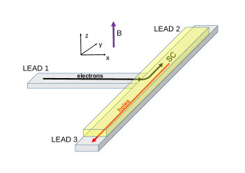
We consider a -shaped device with quasi-one-dimensional leads with Rashba SO interaction and the superconducting pairing in one of the arms induced by a proximity to a superconductor, as depicted schematically in Fig. 1.
In the presence of the magnetic field , the Hamiltonian of the system in the basis is given by
| (1) | |||||
where with , is the effective mass, are the spatially dependent pairing and chemical potential, and with are the Pauli matrices acting on the spin and electron-hole degree of freedom, respectively. The dynamics of the electron spin is additionally determined by the Rashba SO coupling whose strength is defined by the parameter .
In our model, we adopt the following material parameters corresponding to InSb:Gazibegovic et al. (2017) , , meVnm. For the device with induced superconductivity, we consider the induced gap meV as obtained by proximitizing the semiconductor with a thin Al shell Chang et al. (2015). The numerical calculations are performed on a square lattice with nm and nanowire width nm. To determine the normal and Andreev transmission probabilities, we use the Kwant package Groth et al. (2014).
In the proposed nanostructure, electrons are injected from the left lead , which acts as the input, and they either flow out from the device via the upper and lower arms or are reflected back into the input lead (see Fig. 1).
At zero temperature, the nonlocal conductance between the contacts and is given byRosdahl et al. (2018); Anantram and Datta (1996)
| (2) |
where is the number of transverse modes in the lead and are the normal (electron-electron) and Andreev (electron-hole) transmission amplitudes corresponding to the situation when the electron is injected into the lead and flow out from the device as an electron or hole through the lead . For a non-superconducting system, the formula (2) reduces to the standard Landuer-Büttiker formula for a three terminal device Wójcik et al. (2015) with .
III Results
We shall now discuss the nonlocal conductance in the -shaped nanostructure separately in the case with and without the superconducting shell. We put particular emphasis on the detection of the helical gap, which results from the interplay between the Rashba SO coupling and the external magnetic field. We then discuss a possible detection of the topological phase by the nonlocal conductance measurement.
III.1 Helical gap detection
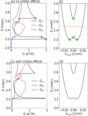
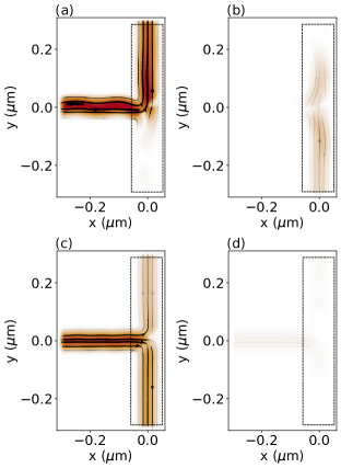
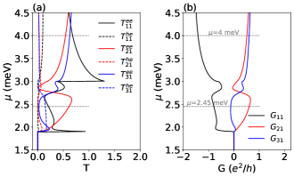
Let us first consider the -shaped junction as in Fig. 1 without the superconducting shell. For the considered nanostructure we set and calculate the nonlocal conductance as a function of the incoming electron energy [see Fig. 2(a)]. In nanowires with strong Rashba SO coupling, the spin-Zeeman effect of the perpendicular magnetic field opens the helical gap. We illustrate this by plotting the dispersion relation for the horizontal (vertical) system lead as presented in Fig. 2(b). In this specific energy range, the spin of an electron is directly coupled to its momentum, so that in particular for one-dimensional nanowires, electrons flowing in opposite directions possess opposite spins. As seen in Fig. 2(a), for the energy range corresponding to the helical gap [compared with panel (b)], the nonlocal conductance dominates over other conductance components. This is a consequence of the preferred electron injection to the upper arm, clearly seen on the current map in Fig. 3(a). Note however, that the preference does not result from the orbital effects of the magnetic field and the corresponding Lorentz force, which are not included here. Results with the inclusion of the orbital effectsorb are presented below in panels Fig. 2(c,d), and do not exhibit any significant difference with respect to those depicted in panels (a),(b). For this reason, henceforth we neglect the orbital effects of the magnetic field.
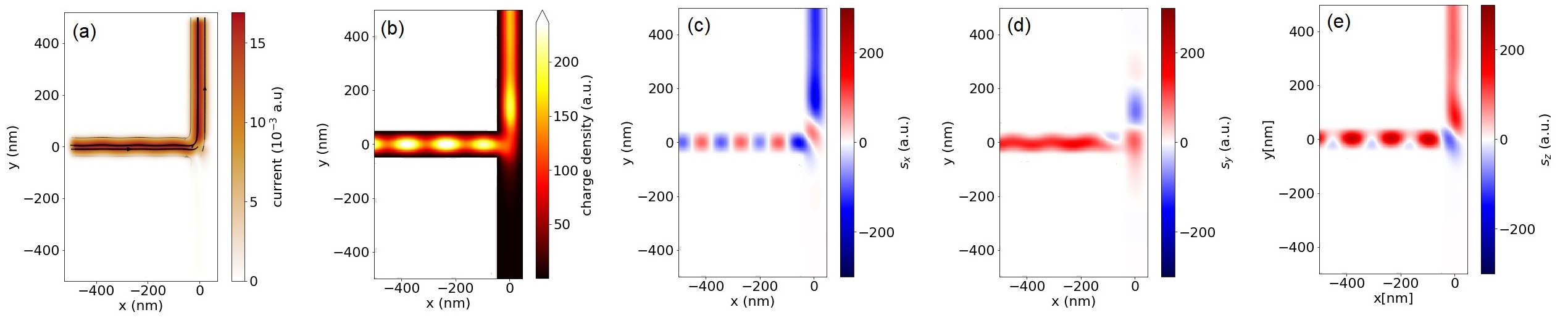
The injection preference presented in Fig. 3 is a consequence of the combined effects of the Rashba SO coupling and the magnetic field and can be explained based on the Heisenberg equation, according to which the second derivative of the position operator , classically interpreted as a force, can be expressed as
| (3) | |||||
Since the force operator depends on the electron spin, which is an internal quantum degree of freedom, it does not have a classical analog. The first term is related to the well-known internal spin Hall effectSinova et al. (2004) whereas the second corresponds to the interplay of the perpendicular magnetic field with the Rashba SO coupling. The physical meaning, i.e., the measurable prediction is contained in the quantum-mechanical expectation value, defined as , with the initial spinor .
For the sake of simplicity, let us now reduce the system to one-dimensional nanowires connected in the -shape geometry. We assume that the electron with energy from the helical gap range is injected into the input lead within the quantum state corresponding to ,
| (4) |
where is the Zeeman energy. It flows through the horizontal NW with the force expectation value , characteristic for all eigenstates. At the fork of the -junction, the electron in the state is injected into the vertical NW for which is not an eigenstate. As a result, is no longer zero and takes the form
| (5) |
with the non-zero component pushing electrons into the upper arm (note that as we assume ). Although increases linearly with the magnetic field, it is non-zero only when the SO coupling is present. Indeed, as shown in Fig. 4(b), for and electrons are injected symmetrically in both the junction arms leading to the equal non-local conductances and .
The strong injection preference is characteristic for the energy range corresponding to the helical gap when the electron in the helical state is injected into the system with a single well-defined vector. In this energy range, the backscattering requires the spin flip, which is energetically less favorable than nearly half spin rotation needed for the injection into the upper arm – see Fig. 3. This, apart from the SO induced force (5), additionally enhances the observed electron injection preference.
For energies outside the helical gap range, electrons can flow in the horizontal NW within two states defined by different wave vectors, characterized by different spin orientations. As such, they are injected into the opposite -junction arms or are backscattered. As a result, the dominance of the conductance is observed solely within the parameter regime (, ) corresponding to the helical gap.
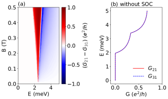
The magnetic field dependence of the nonlocal conductance asymmetry defined as is presented in Fig. 4(a) and clearly indicates the parameter range where the helical gap occurs.
III.2 Topological phase detection
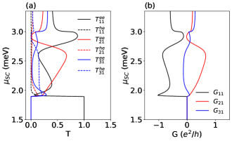
As the nonlocal conductance measurement in the -shaped junction clearly indicates the helical gap range, we now analyze if the same effect can be used to detect the topological superconducting phase which requires the helical gap existenceOreg et al. (2010). For this purpose, we consider the system depicted in Fig. 1 with the superconducting shell covering the fork. The superconducting shell induces electron pairing underneath, in the semiconductor nanowire, and under appropriate conditions the system undergoes the topological phase transition resulting in zero-energy Majorana states localised at the ends of the superconducting section. In this configuration, electrons from the horizontal nanowire are injected directly into the superconducting vertical arm where they can be reflected as holes or transmitted to the leads and as holes or electrons. We assume that the length of the superconducting shell , where is the superconducting coherence length. Note that if the chemical potential is situated in the helical gap in the superconducting nanowire, needed for a topological phase transition, we should observe the nonlocal conductance asymmetry in analogy to Fig. 4(a).
As previously, the electron is injected into the nanostructure from the lead . If its energy lies in the helical gap at the fork, it turns left into the upper arm due to the mechanism described above. Here, if it undergoes the Andreev reflection as a hole with opposite spin [cf. Fig. 5]. The reflected hole is transmitted to lead . Note that due to the finite length of the proximitized region, the Andreev reflection is not perfect, and there is a finite probability for an electron to escape through the lead . This process results in nonzero values of the transmission amplitudes , (and due to the electron reflection from the fork) as can be seen around meV in Fig. 6(a). This in turn results in the pronounced difference of the nonlocal conductances and as presented in Fig. 6(b).
On the contrary, when the system is in a trivial regime (i.e., there is no helical gap in the normal leads and no topological gap in the proximitized region) obtained for meV, the electron current is distributed almost symmetrically among leads 2 and 3. The Andreev reflection is marginal as can be seen in Fig. 5(c) and (d). As a result, the corresponding nonlocal conductances and take similar values depicted in Fig. 6(b). The above shows that the directional electron flow is inherited by the superconducting system provided that it is in the topological superconductivity phase.
So far, we assumed that the -junction can be regarded as a homogeneous system with a constant chemical potential across the nanostructure. The electron injected into the horizontal nanowire within the helical state remains in this helical gap energy range also when it flows through the vertical arm. Note however, that in practice, the assumption of the constant throughout the nanotructure is difficult to fulfill experimentally, as the electronic structure of the vertical nanowire can be affected by the presence of the superconducting shell.
In Fig. 7(a) we present the transmission coefficients for a system where in the normal part we keep a constant value of the chemical potential meV and vary only the chemical potential in the superconducting region. In the range of , in which the proximitized part is in topological phase, we again observe pronounced , amplitudes which results in significant differences in and as presented in Fig. 7(b).
In Fig. 8, the asymmetry of the zero energy nonlocal conductance is clearly apparent in the case (a) when the chemical potential is assumed to be constant throughout the nanostructure or even when (b) the chemical potential in the horizontal nanowire is fixed beyond the helical gap at the energy meV. Note that in the latter case, there are two spin bands available in the input lead . As predicted from the analytical model, Eq. (5), the expectation value of the force depends on at which the electron is injected into the vertical nanowire, which is different for two spin-orbit split bands preserving the asymmetry of the nonlocal conductances and .
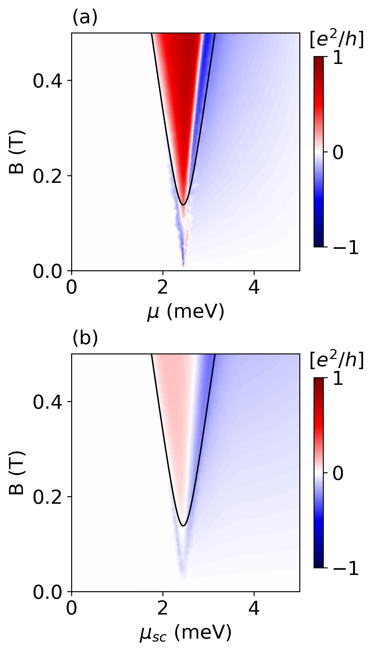
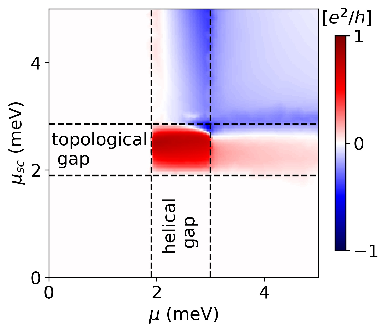
In Fig. 9 we present the asymmetry of the zero-energy nonlocal conductance calculated for a fixed T as a function of the chemical potential in the input nanowire and in the superconducting vertical nanowire . The helical gap range in the input nanowire and the topological gap range in the superconducting nanowire are marked by dashed vertical and horizontal lines, respectively.
As we see, the difference in nonlocal conductance is a clear hallmark of the presence of a topological phase. The conductance asymmetry is obtained regardless of the chemical potential in the horizontal lead and even if the magnetic field is switched off in the horizontal nanowire, preventing helical gap creation in it.
IV Summary and conclusions
Using the scattering matrix approach, we have analyzed transport properties of a -shaped junction characterized by the strong SO coupling. In the presence of a perpendicular magnetic field, we have found that electrons injected with energy in the helical gap regime are turned into the upper arm leading to the remarkable enhancement of the nonlocal conductance. This behavior has been explained within the Heisenberg equation as resulting from the existence of a spin-dependent force which results from the interplay between the SO interaction and the magnetic field. The force pushes electrons with opposite spins into the opposite sides of the nanowire. Specifically, in the helical gap range, when the electron spin is bound to its momentum, the electrons are preferably injected into one of the arms of the -junction. This, as proposed, allows for detection of the helical gap regime by employing nonlocal conductance measurements. As we noticed, the proposed method is free of possible misinterpretations resulting from Fabry-Perrot oscillations present in the two-terminal architecture and local conductance measurements.
Next, by partially covering the -junction by a superconducting shell, we analyze if the same phenomenon can be useful in topological phase detection. We have shown that the nonlocal conductance measurements in the -shaped superconducting junction clearly indicate the topological phase regime even if the chemical potential in both the vertical and horizontal nanowire is not perfectly adjusted.
Note that the calculations presented in the paper do not include the orbital effects. Although in sec. III.1 we have shown that for the considered magnetic field the orbital effects do not play an important role, the investigation of their influence on the superconducting shell and the topological phase is beyond the scope of this paper and was presented in detail in one of our previous papers.Nowak and Wójcik (2018); Wójcik and Nowak (2018)
As a final remark, note that the theoretical predictions presented in this paper should be verifiable within the current state of the art epitaxial technology, which allows for the fabrication of high-quality -shaped, -shaped or hashtag nanowire networks (also with superconducting shells) and performing precise conductance measurementsGazibegovic et al. (2017); T et al. (2017).
V Acknowledgement
This work was supported by National Science Centre (NCN) decision number DEC-2016/23/D/ST3/00394 and by the Romanian Ministry of Research, Innovation and Digitization, CNCS/CCCDI – UEFISCDI, project number PN-III-P1-1.1-TE-2019-0423, within PNCDI III, and partially by PL-Grid and TeraACMiN Infrastructure.
References
- Nadj-Perge et al. (2010) S. Nadj-Perge, S. M. Frolov, E. P. A. M. Bakkers, and L. P. Kouwenhoven, Nature 468, 1084 (2010).
- van den Berg et al. (2013) J. W. G. van den Berg, S. Nadj-Perge, V. S. Pribiag, S. R. Plissard, E. P. A. M. Bakkers, S. M. Frolov, and L. P. Kouwenhoven, Phys. Rev. Lett. 110, 066806 (2013).
- Luo et al. (2011) J.-W. Luo, L. Zhang, and A. Zunger, Phys. Rev. B 84, 121303 (2011).
- Koo et al. (2009) H. C. Koo, J. H. Kwon, J. Eom, J. Chang, S. H. Han, and M. Johnson, Science 325, 1515 (2009).
- Wójcik et al. (2014) P. Wójcik, J. Adamowski, B. J. Spisak, and M. Wołoszyn, J. Appl. Phys. 115, 104310 (2014).
- Wójcik and Adamowski (2017) P. Wójcik and J. Adamowski, Sci Rep 7, 45346 (2017).
- Kohda et al. (2012) M. Kohda, S. Nakamura, Y. Nishihara, K. Kobayashi, T. Ono, J. O. Ohe, Y. Tokura, T. Mineno, and J. Nitta, Nature Communications 3, 1082 (2012).
- Debray et al. (2009) P. Debray, S. M. S. Rahman, R. S. Newrock, M. Muhammad, J. Wan, M. Cahay, A. T. Ngo, S. E. Ulloa, S. T. Herbert, and M. Johnson, Nature Nanotechnology 4, 759 (2009).
- Hofstetter et al. (2009) L. Hofstetter, S. Csonka, J. Nygard, and C. Schönenberger, Nature 461, 960 (2009).
- Das et al. (2012) A. Das, Y. Ronen, M. Heiblum, D. Mahalu, A. V. Kretinin, and H. Shtrikman, Nature Communications 3, 1165 (2012).
- Mourik et al. (2012) V. Mourik, K. Zuo, S. M. Frolov, S. R. Plissard, E. P. A. M. Bakkers, and L. P. Kouwenhoven, Science 336, 1003 (2012).
- Albrecht et al. (2016) S. M. Albrecht, A. P. Higginbotham, M. Madsen, F. Kuemmeth, T. S. Jespersen, J. Nygåard, P. Krogstrup, and C. M. Marcus, Nature 531, 206 (2016).
- Sau et al. (2012) J. D. Sau, S. Tewari, and S. Das Sarma, Phys. Rev. B 85, 1 (2012).
- Dresselhaus (1955) G. Dresselhaus, Phys. Rev. 100, 580 (1955).
- Rashba (1960) E. I. Rashba, Sov. Phys. Solid State 2, 1109 (1960).
- Manchon et al. (2015) A. Manchon, C. Koo, H, J. Nitta, M. Frolov, S, and A. Duine, R, Nature Materials 14, 871 (2015).
- Nadj-Perge et al. (2012) S. Nadj-Perge, V. S. Pribiag, J. W. G. van den Berg, K. Zuo, S. R. Plissard, E. P. A. M. Bakkers, S. M. Frolov, and L. P. Kouwenhoven, Phys. Rev. Lett. 108, 166801 (2012).
- Nowack et al. (2007) K. C. Nowack, F. H. L. Koppens, Y. V. Nazarov, and L. M. K. Vandersypen, Science 318, 1430 (2007).
- van Weperen et al. (2015) I. van Weperen, B. Tarasinski, D. Eeltink, V. S. Pribiag, S. R. Plissard, E. P. A. M. Bakkers, L. P. Kouwenhoven, and M. Wimmer, Phys. Rev. B 91, 201413(R) (2015).
- Campos et al. (2018) T. Campos, P. E. Faria Junior, M. Gmitra, G. M. Sipahi, and J. Fabian, Phys. Rev. B 97, 245402 (2018).
- Iorio et al. (2019) A. Iorio, M. Rocci, L. Bours, M. Carrega, V. Zannier, L. Sorba, S. Roddaro, F. Giazotto, and E. Strambini, Nano Lett. 19, 652 (2019).
- Wójcik et al. (2019) P. Wójcik, A. Bertoni, and G. Goldoni, Appl. Phys. Lett. 114, 073102 (2019).
- Wójcik et al. (2018) P. Wójcik, A. Bertoni, and G. Goldoni, Phys. Rev. B 97, 165401 (2018).
- Wójcik et al. (2021) P. Wójcik, A. Bertoni, and G. Goldoni, Phys. Rev. B 103, 085434 (2021).
- Středa and Šeba (2003) P. Středa and P. Šeba, Phys. Rev. Lett. 90, 256601 (2003).
- Pershin et al. (2004) Y. V. Pershin, J. A. Nesteroff, and V. Privman, Phys. Rev. B 69, 121306 (2004).
- Quay et al. (2010) C. H. L. Quay, T. L. Hughes, J. A. Sulpizio, L. N. Pfeiffer, K. W. Baldwin, K. W. West, D. Goldhaber-Gordon, and R. De Picciotto, Nat. Phys. 6, 336 (2010).
- Heedt et al. (2017) S. Heedt, N. Traverso Ziani, F. Crépin, W. Prost, S. Trellenkamp, J. Schubert, D. Grützmacher, B. Trauzettel, and T. Schäpers, Nature Phys. 13, 563 (2017).
- Rainis and Loss (2014) D. Rainis and D. Loss, Phys. Rev. B 90, 235415 (2014).
- Heyder et al. (2015) J. Heyder, F. Bauer, E. Schubert, D. Borowsky, D. Schuh, W. Wegscheider, J. von Delft, and S. Ludwig, Phys. Rev. B 92, 195401 (2015).
- Pedder et al. (2016) C. J. Pedder, T. Meng, R. P. Tiwari, and T. L. Schmidt, Phys. Rev. B 94, 245414 (2016).
- Kammhuber et al. (2017) J. Kammhuber, M. C. Cassidy, F. Pei, M. P. Nowak, A. Vuik, D. Car, S. R. Plissard, E. P. A. M. Bakkers, M. Wimmer, and L. P. Kouwenhoven, Nat Commun. 8, 478 (2017).
- Fu and Kane (2008) L. Fu and C. L. Kane, Phys. Rev. Lett. 100, 096407 (2008).
- Kitaev (2003) A. Kitaev, Ann. Phys. 303, 2 (2003).
- Oreg et al. (2010) Y. Oreg, G. Refael, and F. von Oppen, Phys. Rev. Lett. 105, 177002 (2010).
- Alicea (2012) J. Alicea, Rep. Prog. Phys. 75, 076501 (2012).
- Das Sarma et al. (2015) S. Das Sarma, M. Freedman, and C. Nayak, npj Quantum Information 1, 15001 (2015).
- Pan and Das Sarma (2020) H. Pan and S. Das Sarma, Phys. Rev. Research 2, 013377 (2020).
- Pan et al. (2021) H. Pan, C.-X. Liu, M. Wimmer, and S. D. Sarma, (2021), arXiv:2102.02218 .
- Nichele et al. (2020) F. Nichele, E. Portolés, A. Fornieri, A. M. Whiticar, A. C. C. Drachmann, S. Gronin, T. Wang, G. C. Gardner, C. Thomas, A. T. Hatke, M. J. Manfra, and C. M. Marcus, Phys. Rev. Lett. 124, 226801 (2020).
- Gazibegovic et al. (2017) A. Gazibegovic, D. Car, H. Zhang, S. C. Balk, J. A. Logan, M. W. A. Moor, M. C. Cassidy, R. Schmits, D. Xu, G. Wang, P. Krogstrup, R. L. M. O. h. Veld, K. Zuo, Y. Vos, J. Shen, D. Bouman, B. Shojaei, D. Pennachio, J. S. Lee, S. V. M. A. Veld-hoven P J v, Koelling, L. P. Kouwenhoven, C. J. Palmstrom, and E. P. A. M. Bakkers, Nature 548, 434 (2017).
- T et al. (2017) F. E. M. T, H. Zhang, S. Conesa-Boj, D. Car, O. Gül, S. R. Plissard, R. L. M. Op het Veld, S. Kölling, L. P. Kouwenhoven, and E. P. A. M. Bakkers, Nano Lett. 17, 6511 (2017).
- Razmadze et al. (2020) D. Razmadze, E. C. T. O’Farrell, P. Krogstrup, and C. M. Marcus, Phys. Rev. Lett. 125, 116803 (2020).
- Chang et al. (2015) W. Chang, S. M. Albrecht, T. S. Jespersen, F. Kuemmeth, P. Krogstrup, J. Nygard, and C. M. Marcus, Nature Nanotechnology 10, 232 (2015).
- Groth et al. (2014) C. W. Groth, M. Wimmer, A. R. Akhmerov, and X. Waintal, New J. Phys. 16, 063065 (2014).
- Rosdahl et al. (2018) T. O. Rosdahl, A. Vuik, M. Kjaergaard, and A. R. Akhmerov, Phys. Rev. B 97, 045421 (2018).
- Anantram and Datta (1996) M. P. Anantram and S. Datta, Phys. Rev. B 53, 16390 (1996).
- Wójcik et al. (2015) P. Wójcik, J. Adamowski, B. J. Spisak, and M. Wołoszyn, J. Appl. Phys. 118, 014302 (2015).
- (49) The orbital effects of the magnetic field are incorporated using Peierls substitution of the hopping elements .
- Sinova et al. (2004) J. Sinova, D. Culcer, Q. Niu, N. A. Sinitsyn, T. Jungwirth, and A. H. MacDonald, Phys. Rev. Lett. 92, 126603 (2004).
- Nowak and Wójcik (2018) M. P. Nowak and P. Wójcik, Phys. Rev. B 97, 045419 (2018).
- Wójcik and Nowak (2018) P. Wójcik and M. P. Nowak, Phys. Rev. B 97, 235445 (2018).