Voltage-Controlled Reconfigurable Magnonic Crystal at the Submicron Scale
Abstract
Multiferroics offer an elegant means to implement voltage-control and on the fly reconfigurability in microscopic, nanoscaled systems based on ferromagnetic materials. These properties are particularly interesting for the field of magnonics, where spin waves are used to perform advanced logical or analogue functions. Recently, the emergence of nano-magnonics is expected to eventually lead to the large-scale integration of magnonic devices. However, a compact voltage-controlled, on demand reconfigurable magnonic system has yet to be shown. Here, we introduce the combination of multiferroics with ferromagnets in a fully epitaxial heterostructure to achieve such voltage-controlled and reconfigurable magnonic systems. Imprinting a remnant electrical polarization in thin multiferroic with a periodicity of yields a modulation of the effective magnetic field in the micron-scale, ferromagnetic magnonic waveguide. We evidence the magneto-electrical coupling by characterizing the spin wave propagation spectrum in this artificial, voltage induced, magnonic crystal and demonstrate the occurrence of a robust magnonic bandgap with rejection.
Spin waves, the collective spin excitations in a magnetically ordered material and their associated quanta, magnons, are promising candidates to be used as information carriers for the next generation of information processing devices 1; 2; 3. Among all beyond-CMOS (complementary metal-oxide semiconductor) based approaches, magnonics combines room-temperature operation at GHz frequencies, nano-scale integration, digital and analog architectures 4; 5; 6; 7. Magnons can interact directly or indirectly with frequencies from the microwave to the optical regime. Thus, magnonics enables the coupling to other paradigms such as quantum computing and opto-electronics rendering it a rich playground to test innovative ideas to overcome the power consumption bottleneck of conventional CMOS-based electronics 8; 9; 10; 11; 12; 13; 14. However, the compatibility with state of the art CMOS based technologies will still be required for any practical magnonic device. Therefore, signal transducing and processing should be advantageously performed through voltage rather than current driven signals. Correspondingly, piezo-electric transducers and modulators have been proposed 15; 16. In wave-based devices, signal processing most often relies on artificial crystals. Magnonic artificial crystals (MACs) have therefore been extensively studied 17; 18; 19; 20; 21. Achieving reconfigurability has however proven to be difficult. Indeed, most practical realisations of MACs are based on a periodic structuration which prohibits any reconfiguration of the frequency response. To date, reconfigurability has only been demonstrated in a few cases relying on the magnetic stray field modulation, albeit the spatial period of the MAC is fixed by construction 22; 23; 24.
Recently, theoretical propositions based on micromagnetic simulations have shown the interest of voltage-controlled reconfigurable MAC 25. Such devices based on the switching of multiferroic domain states would simultaneously allow for electric field control and low-power operation 26; 27.
Here, we present a fully reconfigurable, voltage-controlled device which passively couples magnonics to the magneto-electric degrees of freedom in a multiferroic/ferromagnetic heterostructure (Fig. 1) and operates at .
Regarding the multiferroic, we employ a thick layer of (BFO). This material is one of the most studied multiferroics and exhibits both a sizeable magneto-electric coupling and a piezo-electric effect of 28; 29; 30; 31; 32; 33.
For the ferromagnetic layer which serves as the spin wave medium, we utilize a thick layer of (LSMO) 34.
Based on this structure, we create our reconfigurable and tuneable crystal by using the piezo-force microscopy (PFM) technique to generate a uniformly or periodically polarized ferroelectric pattern in the BFO 35; 36. In turn that pattern modulates the spin wave propagation in the LSMO, and allows to obtain spin wave filtering at the magnonic bandgap of the crystal.
We identify the creation of the bandgap —the hallmark of a magnonic crystal —by a careful comparison of the transmitted spin wave spectra whilst the adjacent ferroelectric domain state is changed between a uniform down (virgin) or up or periodically down-up ferroelectric polarization. That comparison (cf. Fig. 2) allows us to unambiguously attribute the observed frequency filtering (cf. Fig. 3) in the amplitude representation at to a bandgap in the magnonic medium due to the periodic domain configuration of BFO. In our study we show the modulation of the spin wave propagation by applying a voltage to the BFO layer which switches the ferroelectric polarization states. Our conceptual realization of such voltage control allows for other perspectives to go beyond PFM based writing. For instance, the theoretical propositions for all-solid state devices discussed by the work of Q. Wang et al. 25 can be adapted to the BFO polarisation control using an array of voltage-gates. Writing or erasing the MAC could be simply performed using voltage spikes on a desired set of electrodes.
Results and Discussion
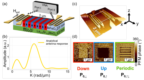
The device layout and experimental setup for the creation of a reconfigurable magnonic crystal with our multiferroic/ferromagnetic BFO/LSMO heterostructure are shown in Fig. 1. In order to maximize the influence of the BFO interfacial polarization state we minimized the thickness of the LSMO layer to where the growth conditions are optimized such that the dynamical magnetic properties are improved. For instance, we obtained a value of for the Gilbert damping parameter which is comparable to that of thicker films 37.
Further details on growth and the nanofabrication process are given in the methods section and section 1 of the supporting information (cf. Fig. S1). We excite and detect spin waves in the Damon-Eshbach configuration 38 by means of propagative spin wave spectroscopy 39 (cf. Fig. 1 (a)) and deduce the transmission inductance parameter from the recorded data (cf. Supporting information). In order to both write and read the ferroelectric domain configuration of BFO, we employ piezo-force microscopy (PFM) to define the out-of-plane polarization state between the microwave antennae within an area of (cf. Fig. 1 (d)). The number of the writing steps starting from the virgin state is labelled as , where denotes the writing cycle defined as the sequence of virgin, up, periodic domain polarization states and m the specific configuration in that writing cycle. The antenna arms exhibit a periodicity of . Hence, the antennae predominantly excite spin waves around corresponding to a maximum of the antenna’s response spectrum (cf. Fig. 1 (b)). Therefore, the present study focuses on a periodic ferroelectric domain pattern with the same periodicity of . The resulting Bragg wavevector of the periodic ferroelectric pattern then corresponds to spin waves of the wave vector of , where the down and up domains have a width of and , respectively. Matching the periods of the antennae and the ferroelectric domains allows to set the bandgap at the most efficiently excited wavevector. Consequently, such a matching optimizes the coupling between the antennae and supports the unambiguous interpretation of the results.
Please note, that at room temperature spin wave excitations in BFO occur in the sub-THz 40 band and cannot be coherently excited here. Thus, any observation of a spin wave transmission signal can be fully attributed to the spin wave excitation in the LSMO layer.
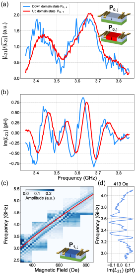
Fig. 2 (a) and (b) shows the inductance signal of the spin wave for the two uniform up (red) and down polarized (blue) ferroelectric domain states in the BFO layer for the amplitude (in linear scale) and the imaginary part, respectively. The initial (virgin) down state is compared to the up state.
Apart from small shifts in resonance frequency,
there is no change between both uniform up and down ferroelectric domain states in the BFO indicating that the PFM writing process does not affect the LSMO properties. We attribute the small frequency difference to a slight misalignment of the sample with respect to the magnetic field between different PFM writing cycles.
Furthermore, since we used less averaging cycles for the S-parameters during the measurement, the noise floor of the virgin state is higher than for the uniform up (cf. Fig. 2 b) state. Hence, by the comparison of the two different uniform ferroelectric polarization states before writing a periodic structure (cf. Fig. 2 a-b) and after rewriting back to a uniform state (cf. Fig. 2 c-d), we can reliably and reproducibly switch between the various ferroelectric polarization domain states which are also temporally stable.
In order to model the dispersion relation (cf. Fig. 2 (c), red line) for our system, we utilize the approach developed by B.A. Kalinikos and A. N. Slavin 41; 42 by considering both an in-plane (ip) and out-of-plane (oop) (uniaxial) anisotropy for spin waves in the Damon-Eshbach configuration which reads as:
| (1) |
where with for the in-plane (ip) anisotropy field
and (: external field, : demagnetization field, : exchange length, , wave vector of spin wave), , (, w: width of waveguide), the in-plane angle between the saturation magnetization (here along the y-axis) and the waveguide axis (x-axis), N, where denotes the out-of-plane anisotropy field, N and the matrix elements (t: ferromagnetic layer thickness) 41.
The modeled dispersion is shown (red solid line) (, , , , , an offset taking additional contributions to the effective field and uncertainties in the determination of the saturation magnetization into account) together with the recorded dependence of for the lowest mode number and at in Fig. 2 c-d for the -BFO domain state.
By employing ferromagnetic resonance, we find and a Gilbert damping as low as of our 13 nm thick LSMO layer (Supporting information section 2 (cf. Fig. S2)). Furthermore, the low value of allows us to extend the distance between the emitting and receiving antennae for the spin wave transmission signal to the micrometre range. In a similar fashion to Ref. 39 we can both theoretically and experimentally estimate the spin wave attenuation length of our system. Theoretically, for
, group velocity estimated from our dispersion relation and , we obtain , where is the lifetime defined as . We experimentally estimate the attenuation length from the decay of the spin wave amplitude, i.e. , where corresponds to the effective distance between the antennae, with the antenna spacing denoted as and as the width of the antennae arms, respectively. Then, we obtain very close to the theoretically expected value which validates the overall modeling approach.
As a result, the study of the spin wave dispersion spectrum allows now to directly attribute changes in the spin wave transmission signal for periodically altered ferroelectric domains to a periodic modulation, i.e. the emergence of a bandgap (cf. Fig. 3).
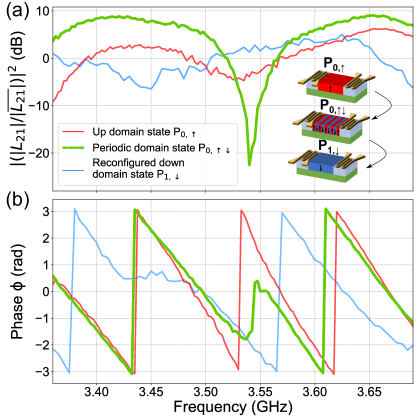
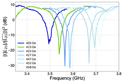
In Fig. 3 (a)-(b), we show the transmitted spin wave’s envelope (amplitude, (a)) and phase ((b)) in the LSMO layer from the measurement for the periodic arrangement of up and down polarized ferroelectric domains in the BFO layer (green) and compare it both to the uniformly up polarized state (red) and reconfigured down polarized state (blue). At (cf. Fig. 3 (a)), the spin wave amplitude drops by compared to the amplitude in the uniformly up polarized case. Further, at that frequency, we also observe an additional phase jump in the phase spectrum for the case of the periodic domain pattern. The occurrence of such an additional phase jump was not observed for the uniform ferroelectric domains of the BFO layer, where both amplitude and phase show no discontinuity over the measured frequency window. In particular, the gap and the corresponding phase discontinuity due to the change in group velocity vanish by the following reconfiguration of the system back to the uniform FE polarization state. Furthermore, both the frequency of the gap and the phase jump are field dependent. As illustrated in Fig. 4 we observe a shift to higher frequencies according to the dispersion relation, when the external magnetic field is increased, confirming the bandgap with a strong amplitude rejection exceeding .
.
The propagative spin wave spectroscopy used here does not provide direct access to the wavevector of the excited spin wave. However, it is possible to infer the wavevector through the phase of the dynamical magnetization . It depends on the wavevector via , i.e. is described as a plane wave, which allows us to assess discontinuities in the dispersion of a MAC. The distance from the antenna exciting the spin wave which propagates to the second, receiving antenna is . As a result, the accumulated phase between and corresponds to . Then, the frequency dependence of wavevector can be derived from the unwrapped phase (typically the VNA measures the wrapped phase) by , where is an integration constant that is set by the phase of the excitation field.
However, by introducing a spacial periodicity, we expect the dispersion relation to split in different branches separated by a magnonic band gap.
Interestingly in the vicinity of (the MAC’s Bragg wavevector) the phase relation established previously no longer holds due the branches degeneracy. Indeed, the reflections induced by the periodic domains strongly interfere near the band gap (Bragg conditions). Standing spin-waves are formed, thus the plane wave ansatz does not hold anymore. Additionally, the position of those standing waves can abruptly change the coupling with the antennas and the value when they move from the lower to the upper dispersion branch. Hence, the step-like phase jump for the MAC ( state) is reminiscent of an additional large phase accumulation, probably much larger than as the 20dB drop in the transmitted amplitude indicates. Measuring the value of this phase-jump would require a time-resolved measurement scheme.
Our observations demonstrate that a change in the ferroelectric state unquestionably modulates the spin wave dispersion of the ferromagnetic layer.
However, the underlying governing physical mechanism that couples the polarisation state of BFO and LSMO is still to be identified.
The most probable mechanism would imply the coupling of the ferroelectric state to the antiferromagnetic order in BFO that induces a modulation of an the interfacial exchange field. As a matter of fact BFO/LSMO heterostructures are known to exhibit magneto-electric control of the exchange bias field (up to at ) but this field vanishes when the temperature is increased on macroscopic devices towards room temperature 43; 44. However, given the small sizes of the written ferroelectric domains ( and ) in our system, it is possible that there is a remanent exchange coupling between BFO and LSMO that is sufficient in amplitude to generate a MAC and enables the observed frequency filtering.
Correspondingly, as well as a thickness dependent study of the LSMO layer in addition to the modulation of the ferroelectric polarization of the BFO and a temperature dependent study on the role of the exchange bias could give further insight into the relevance of these effects and the role of the interface for these types of oxide heterostructures.
Conclusion
In summary, we implemented a tuneable MAC filtering scheme based on BFO/LSMO thin film heterostructures. Our approach allows us to reliably and reversibly filter certain frequencies in the spin wave dispersion, analogous to magnonic crystals, by controlling the ferroelectric domain state order of the BFO layer. Once written in a certain domain pattern., no further energy input is required in the MAC filtering, which results in minimal power consumption for the operation of our device. Furthermore, the writing voltage does not exceed . Thus, the introduction of multiferroics, reconfigurable and low power voltage controlled materials into microscopic magnonic systems represents a key step towards large scale integrated magnonic systems.
Methods
Growth
Both LSMO and BFO are perovskites with well-matched unit cell parameters. They are epitaxially grown on an NGO substrate using pulsed laser deposition (PLD) 45. Please note, that in order to reduce leakage effects of the film between the electrode and the PFM tip, the BFO layer is not pure BFO but has been doped with of Manganese (Mn). Regarding the growth conditions, the BFO/ LSMO //NGO (001) is grown by pulsed laser ablation under oxygen-rich growth conditions of and for the LSMO film, and and for the BFMO film. The frequency of the laser is and , respectively. Annealing at is carried after the growth of the bilayer for minutes in an environment rich in oxygenates ().
Device fabrication
For the fabrication of our device we employed a combination of laser lithography and electron ion beam machining for the smallest structures such as the microwave antennae. As for the waveguide’s dimensions it exhibits a width of and length of . A thin () alumina oxide () layer is sandwiched between the BFO and a titanium () layer. The titanium layer enhances the adhesion of the gold for the addition of the microwave antennae for the propagative spin wave spectroscopy. These antennae (Au, ) exhibit a meander-like structure with a periodicity of with several periods narrowing the wavevector band of excited spin waves.
Propagative spin wave spectroscopy
The spin wave spectra are obtained via probe-tip ferromagnetic resonance. The resulting transmission and reflection scattering matrix is recorded by means of network analysis employing a two-port (i and j) vector network analyzer setup.
Supporting information
We have provided supporting information for our work which is available online. The contents are:
-
•
Material’s characterizations including a RHEED diffraction pattern.
-
•
Information on the measured scattering parameters and deduced inductance matrix
-
•
Characterization of dynamic magnetic properties: Ferromagnetic resonance measurements of the unpatterned BFO/LSMO bilayer.
Acknowledgements
This work has been supported from the European Union’s Horizon 2020 research and innovation program within the FET-OPEN project CHIRON under grant agreement No. 801055. VH is grateful for support from the project OISO under grant agreement ANR-17-CE24-0026 from the Agènce National de la Recherche.
Author contributions
V.H and C.C. grew and characterized the sample with H.M. H.M, L.V.patterned the devices. I.B and H.M characterized the devices and conducted the measurements. I.B, H.M, M.A analysed the data and wrote the manuscript. A.V., S. F and V.G. performed the PFM characterization and writing. M.A., A.B., P.B. and M.B. supervised the project. All authors discussed the results and participated in the preparation of the manuscript.
References
- (1) Lenk, B., Ulrichs, H., Garbs, F. & Münzenberg, M. The Building Blocks of Magnonics. Phys. Rep. 2011, 507, 107–136 .
- (2) Kruglyak, V. V., Demokritov, S. O. & Grundler, D. Magnonics. J. Phys. D 2010, 43, 260301.
- (3) Khitun, A., Bao, M. & Wang, K. L. Magnonic Logic Circuits. J. Phys. D 2010, 43, 264005.
- (4) Kostylev, M. P., Serga, A. A., Schneider, T., Leven, B. & Hillebrands, B. Spin - Wave Logical Gates. Appl. Phys. Lett. 2005, 87, 153501.
- (5) Schneider, T., Serga,A. A. , Leven, B. , Hillebrands, B., Stamps,R. L., Kostylev,M. P., Realization of Spin - Wave Logic Gates. Appl. Phys. Lett. 2008, 92, 022505.
- (6) Zografos, O., Manfrini, M. , Vaysset, A., Sorée, B., Ciubotaru, F., Adelmann, C., Lauwereins, R., Raghavan, P. and Radu, I. P. Exchange - Driven Magnetic Logic. Sci. Rep. 2017, 7, 12154.
- (7) Ustinov, A. B., Drozdovskii, A. V. & Kalinikos, B. A. Multifunctional Nonlinear Magnonic Devices for Microwave Signal Processing. Appl. Phys. Lett. 2010, 96, 142513.
- (8) Y. Tabuchi, S. Ishino, A. Noguchi, T. Ishikawa, R. Yamazaki, K. Usami, Y. Nakamura. Coherent Coupling between a Ferromagnetic Magnon and a Superconducting Qubit. Science 2015, 349, 405–408.
- (9) Lachance-Quirion, D., Tabuchi, Y., Gloppe, A., Usami, K. & Nakamura, Y. Hybrid Quantum Systems Based on Magnonics. Appl. Phys. Express 2019, 12, 070101.
- (10) Lachance-Quirion, D., Wolski, S. P., Tabuchi, Y., Kono, S., Usami, K., Nakamura, Y. Entanglement-Based Single-Shot Detection of a Single Magnon with a Superconducting Qubit. Science 2020, 367, 425–428.
- (11) Kusminskiy, S. V., Tang, H. X. & Marquardt, F. Coupled Spin-Light Dynamics in Cavity Optomagnonics. Phys. Rev. A 2016, 94, 033821.
- (12) Parvini, T. S., Bittencourt, V. A. S. V. & Kusminskiy, S. V. Antiferromagnetic Cavity Optomagnonics. Phys. Rev. Research 2020, 2, 022027.
- (13) Chumak , A. V., Vasyuchka, V. I., Serga, A. A. & Hillebrands, B. Magnon Spintronics. Nat. Phys. 2015, 11, 453–461.
- (14) Chumak,A. V. Fundamentals of Magnon-Based Computing 2019, eprint 1901.08934. arXiv. https://arxiv.org/abs/1901.08934v1 ( accessed January 24, 2019)
- (15) Duflou, R., Ciubotaru, F., Vaysset, A., Heyns, M., Sorée, B., Radu, I.P. and Adelmann, C. Micromagnetic Simulations of Magnetoelastic Spin Wave Excitation in Scaled Magnetic Waveguides. Appl. Phys. Lett. 2017, 111, 192411.
- (16) Sadovnikov, A., Grachev, A. A., Sheshukova, S. E., Sharaevskii, Y. P. ,Serdobintsev, A. A. ,Mitin, D. M.& Nikitov, S. Magnon Straintronics: Reconfigurable Spin-Wave Routing in Strain-Controlled Bilateral Magnetic Stripes. Phys. Rev.Lett. 2018, 120, 257203.
- (17) Chumak, A. V., Serga, A. A. & Hillebrands, B. Magnonic Crystals for Data Processing. J. Phys. D 2017, 50, 244001.
- (18) Qin, H., Both, G.-J., Hämäläinen, S. J., Yao, L. & van Dijken, S. Low-Loss YIG-Based Magnonic Crystals with Large Tunable Bandgaps. Nat. Commun. 2018, 9, 5445.
- (19) Frey, P., Nikitin, A. A. , Bozhko, D. A., Bunyaev, S. A., Kakazei, G. N., Ustinov, A. B. , Kalinikos, B. A., Ciubotaru, F., Chumak, A. V., Wang, Q., Tiberkevich, V. S. , Hillebrands, B. and Serga, A. A. Reflection-Less Width-Modulated Magnonic Crystal. Commun. Phys. 2020, 3, 17.
- (20) Choudhury, S., Chaurasiya, A. K. , Mondal, A. K. , Rana, B., Miura, K., Takahashi, H. , Otani, Y., Barman, A. Voltage Controlled On-Demand Magnonic Nanochannels. Sci. Adv. 2020, 6, eaba5457.
- (21) Merbouche, H., Collet, M. , Evelt, M. , Demidov, V. E. , Prieto, J. L., Muñoz, M. , Ben Youssef, J., de Loubens, G., Klein, O. , Xavier, S. , d’Allivy Kelly, O. , Bortolotti, Paolo , Cros, V. , Anane, A., Demokritov, S. O. Frequency Filtering with a Magnonic Crystal Based on Nanometer-Thick Yttrium Iron Garnet Films. ACS Appl. Nano Mater. 2021, 4, 121-128.
- (22) Chumak, A. V., Neumann, T., Serga, A. A., Hillebrands, B. & Kostylev, M. P. A Current-Controlled, Dynamic Magnonic Crystal. J. Phys. D 2009, 42, 205005.
- (23) Topp, J., Heitmann, D., Kostylev, M. P. & Grundler, D. Making a Reconfigurable Artificial Crystal by Ordering Bistable Magnetic Nanowires. Phys. Rev. Lett. 2010, 104, 207205.
- (24) Krawczyk, M. & Grundler, D. Review and Prospects of Magnonic Crystals and Devices with Reprogrammable Band Structure. J. Phys. Condens. Matter 2014, 26, 123202.
- (25) Wang, Q., Chumak, A. V., Jin, L., Zhang, H., Hillebrands, B., Zhong, Z. Voltage-Controlled Nanoscale Reconfigurable Magnonic Crystal. Phys. Rev. B 2017, 95, 134433.
- (26) Hu, Z., Wang, X., Nan, T., Zhou, Z., Ma, B., Chen, X., Jones, J. G., Howe, B. M., Brown, G. J., Gao, Y., Lin, H., Wang, Z., Guo, R., Chen, S., Shi, X., Shi, W., Sun, H., Budil, D., Liu, M. and Sun, N. X. Non-Volatile Ferroelectric Switching of Ferromagnetic Resonance in NiFe/PLZT Multiferroic Thin Film Heterostructures. Sci. Rep. 2016, 6, 32408.
- (27) Rana, B. & Otani, Y. Towards Magnonic Devices Based on Voltage-Controlled Magnetic Anisotropy. Commun. Phys. 2019, 2, 90.
- (28) Ramesh, R. & Spaldin, N. A. Multiferroics: Progress and Prospects in Thin Films. Nat. Mater. 2007, 6, 21–29.
- (29) Sando, D., Barthélémy, A. & Bibes, M. BiFeO3 Epitaxial Thin Films and Devices: Past, Present and Future. J. Phys. Condens. Matter 2014, 26, 473201.
- (30) Park, J.-G., Le, M. D., Jeong, J. & Lee, S. Structure and Spin Dynamics of Multiferroic BiFeO3. J. Phys. Condens. Matter 2014, 26, 433202.
- (31) Garcia, V., Bibes, M. & Barthélémy, A. Artificial Multiferroic Heterostructures for an Electric Control of Magnetic Properties. C. R. Phys. 2015, 16, 168–181.
- (32) Spaldin, N. A. Multiferroics: Past, Present, and Future. MRS Bull. 2017, 42, 385–390.
- (33) Spaldin, N. A. & Ramesh, R. Advances in Magnetoelectric Multiferroics. Nat. Mater. 2019, 18, 203–212.
- (34) Hemberger, J., Krimmel, A., Kurz, T., Krug von Nidda, H.-A., Ivanov, V. Yu., Mukhin, A. A., Balbashov, A. M. , Loidl, A. Structural, Magnetic, and Electrical Properties of Single-Crystalline . Phys. Rev. B 2002, 66, 094410.
- (35) Alexe, M. Nanoscale Characterisation of Ferroelectric Materials : Scanning Probe Microscopy Approach (Springer Berlin Heidelberg, Berlin, Heidelberg, 2004).
- (36) Gruverman, A., Alexe, M. & Meier, D. Piezoresponse Force Microscopy and Nanoferroic Phenomena. Nat. Commun. 2019, 10, 1661.
- (37) Madon, B., Kang,H. B., Kang,M.G., Maurya,D. , Magill,B.A., Alves,M. J. P. , Wegrowe,J.-E., Drouhin,H.-J., Priya,S. and Khodaparast,Giti A. Room Temperature Ferromagnetic Resonance in Hetero-Epitaxial BTO - BFO/LSMO Magnetoelectric Composite. AIP Adv. 2018, 8, 105034.
- (38) Damon, R. & Eshbach, J. Magnetostatic Modes of a Ferromagnetic Slab. J. Phys. Chem. Solids 1961, 19, 308–320.
- (39) Vlaminck, V. & Bailleul, M. Spin-Wave Transduction at the Submicrometer Scale: Experiment and Modeling. Phys. Rev. B 2010, 81, 014425.
- (40) Białek, M., Murk, A. & Ansermet, J.-Ph. Spin-Wave Resonances in Bismuth Orthoferrite at High Temperatures. Phys. Rev. B 2018, 97, 054410.
- (41) Kalinikos, B. A. & Slavin, A. N. Theory of Dipole-Exchange Spin Wave Spectrum for Ferromagnetic Films with Mixed Exchange Boundary Conditions. J. Phys. C 1986, 19, 7013–7033.
- (42) Kalinikos, B. A., Kostylev, M. P., Kozhus, N. V. & Slavin, A. N. The Dipole-Exchange Spin Wave Spectrum for Anisotropic Ferromagnetic Films with Mixed Exchange Boundary Conditions. J. Phys. Condens. Matter 1990, 2, 9861–9877.
- (43) Wu, S. M., Cybart, Shane A., Yu, P., Rossell, M. D., Zhang, J. X., Ramesh, R. and Dynes, R. C. Reversible Electric Control of Exchange Bias in a Multiferroic Field-Effect Device. Nat. Mater. 2010, 9, 756–761.
- (44) Yi, D., Yu, P., Chen, Y.-C., Lee, H.-H., He, Q., Chu, Y.-H. and Ramesh, R. Tailoring Magnetoelectric Coupling in BiFeO3/La0.7Sr0.3MnO3 Heterostructure through the Interface Engineering. Adv. Mater. 2019, 31, 1806335.
- (45) Béa, H., Bibes, M., Cherifi, S., Nolting, F., Warot-Fonrose, B., Fusil, S., Herranz, G., Deranlot, C., Bouzehouane, K. and Barthélémy, A. Tunnel Magnetoresistance and Robust Room Temperature Exchange Bias with Multiferroic BiFeO3 Epitaxial Thin Films. Appl. Phys. Lett. 2006, 89, 242114.