Wafer-scale, epitaxial growth of single layer hexagonal boron nitride on Pt(111)
Abstract
Single layer hexagonal boron nitride is produced on 2 inch Pt(111)/sapphire wafers. The growth with borazine vapour deposition at process temperatures between 1000 and 1300 K is in-situ investigated by photoelectron yield measurements. The growth kinetics is slower at higher temperatures and follows a law which better fits for higher temperatures. The crystal-quality of h-BN/Pt(111) is inferred from scanning low energy electron diffraction (x-y LEED). The data indicate a strong dependence of the epitaxy on the growth temperature. The dominant structure is an aligned coincidence lattice with 10 -BN on 9 Pt(11) unit cells and follows the substrate twinning at the millimeter scale.
keywords:
Hexagonal boron nitride, CVD growth on catalysts, in-situ photoelectron yield measurements, growth kinetics, wafer scaleContributed equally to this work \altaffiliationContributed equally to this work \phone+41 44 635 57 44
1 Introduction
Two-dimensional (2D) materials are expected to become important for the application of concepts for platforms and building blocks in electronic devices beyond the silicon technology 1, 2, in nanophotonics 3, in membrane technology 4, for mechanical detectors 5 or as interface systems in electrochemical environments 6. All these promises rely on the production of the materials at large scale and in sufficient quality. Quality as a degree of excellence may have several aspects, like crystallinity, homogeneity, stoichiometry, defect density etc., after growth, transfer or processing. In the present contribution to this focus on hexagonal boron nitride (-BN) we report advances and challenges of epitaxial growth of single layer -BN with chemical vapour deposition (CVD) in ultra-high vacuum (UHV) environment and pick platinum as a prototype growth substrate. The crystal-quality after growth is quantified from low energy electron diffraction patterns.
There are excellent reviews on CVD grown single layer -BN, covering applications in surface science 7 and beyond 8. First reports on the adsorption of borazine on Pt(111) and Ru(0001) surfaces date back to 1990: Paffett et al. reported ordered close-packed -BN overlayers with saturation BN coverages corresponding to one monolayer of -BN 9. Work with other precursor molecules like trichloroborazine 10 revealed, compared to the 10 on 9 coincidence lattice 9 a low energy electron diffraction (LEED) pattern rotated by 30 degrees 11. The -BN/Pt(111) system was further investigated with low energy electron microscopy (LEEM) that gave direct insight into the growth kinetics which is based on a nucleation and growth mechanism 12.
For many applications -BN has to be transferred from the growth substrate, where exfoliation from Pt was demonstrated in 2013 13. The choice of the optimal substrate for growth and exfoliation depends on the bond strength of BN to the substrate, where strong bonding favours the single crystallinity of the -BN, though strong bonding might be a disadvantage if it comes to exfoliation. The dependence of the -BN bond strength to a given substrate 14 and the registry of the BN 15 was predicted by density functional theory (DFT). E.g. comparison between Pt and Ru indicates a weaker binding of BN to platinum 14, 16, though it appears more difficult to grow single orientation -BN on Pt 17 as compared to Ru 18.
Upscaling is a further requirement for material production and was first addressed with the use of single crystalline films as growth substrates 19. This opened the perspective on high quality single orientation layers of -BN on the four inch wafer scale 20. Here we apply Pt(111) on 2 inch wafers as substrates and optimize the growth conditions. A high-temperature growth route facilitates diffusion and stitching of coalescing islands, while using a low pressure of borazine minimizes nucleation seed densities and is necessary to promote systems with minimal residual defect numbers 21. The -BN quality is judged from in-situ monitoring of the growth kinetics at different temperatures with photoelectron yield measurements and the crystal-quality of LEED patterns that are recorded after growth.
2 Methods
2.1 Preparation of the Pt(111)/sapphire wafers
The platinum thin film preparation follows a scheme reported previously 22. Double polished, epi-ready, c-plane, two-inch sapphire wafers were cleaned in H3PO4/H2SO4 (1:3) at 200∘C for 20 min and rinsed in ultra pure water for 3 min in an overflow rinse bath. The sapphire substrates were dried using the Marangoni drying effect. Next, a 500 nm thick Pt layer was deposited on sapphire using e-beam evaporation at 550∘C with an evaporation rate of 0.02-0.03 nm/s. The base pressure of the deposition tool was about mbar.
2.2 Growth and characterization of h-BN/Pt(111)
The single layer -BN is grown in an ultra-high vacuum, chemical vapour deposition (CVD) cold wall chamber for wafers up to 4-inch and was described previously 20. Prior to all -BN preparations the Pt/sapphire substrate was cleaned by argon sputtering, O2 exposure and annealing cycles to 1123 K until sharp Pt(111) () LEED patterns were observed. Subsequently, -BN was prepared at different substrate temperatures above 1000 K with borazine (HBNH)3 as precursor gas at a partial pressure reading of 10-7 mbar. At these conditions single layer growth without hydrogen incorporation is expected. X-ray photoelectron spectroscopy (XPS) on 1010 mm2 samples cut from the 2-inch wafers confirm this and for the presented growth parameters stoichiometric single layer boron nitride was found. The sample temperature was measured with a two-color pyrometer (Maurer, QKTRD 1075). The growth kinetics was traced with photoelectron yield measurements with a xenon flash lamp 23, where photoelectron pulses on an area of 1 cm2 were detected at a rate of about 0.6 Hz with a Keithley 2635A source-measure unit. After growth the structures were investigated in the same apparatus with an OCI BDL600-MCP LEED optics where the diffraction patterns were recorded with a (PCO AG) CCD camera. The cycle time for moving the x-y stage and taking an image was 1.2+0.3 s for positioning and CCD exposure.
3 Results and Discussion
3.1 -BN/Pt(111) growth kinetics
The CVD growth of -BN on transition metals proceeds via nucleation and growth, as it was observed with scanning tunneling microscopy (STM) for -BN/Ni(111) 24 or Rh(111) 25 and with LEEM for -BN/Pt(111) 12 or Ru(0001) 26. The -BN layer grows from homogeneously distributed nucleation centers. Later, the corresponding -BN islands coalesce under further precursor gas exposure to a closed layer. Here we apply photoelectron yield measurements 23 for the direct recording of the growth kinetics. Compared to STM or LEEM this method is low cost and more robust in view of temperature and pressure compatibility. The in-situ surface probing and an overview of the growth process is sketched in Figure 1. An ultraviolet light flash excites photoelectrons, which are collected with a biased antenna, where the detected electron yield is directly related to the -BN coverage .
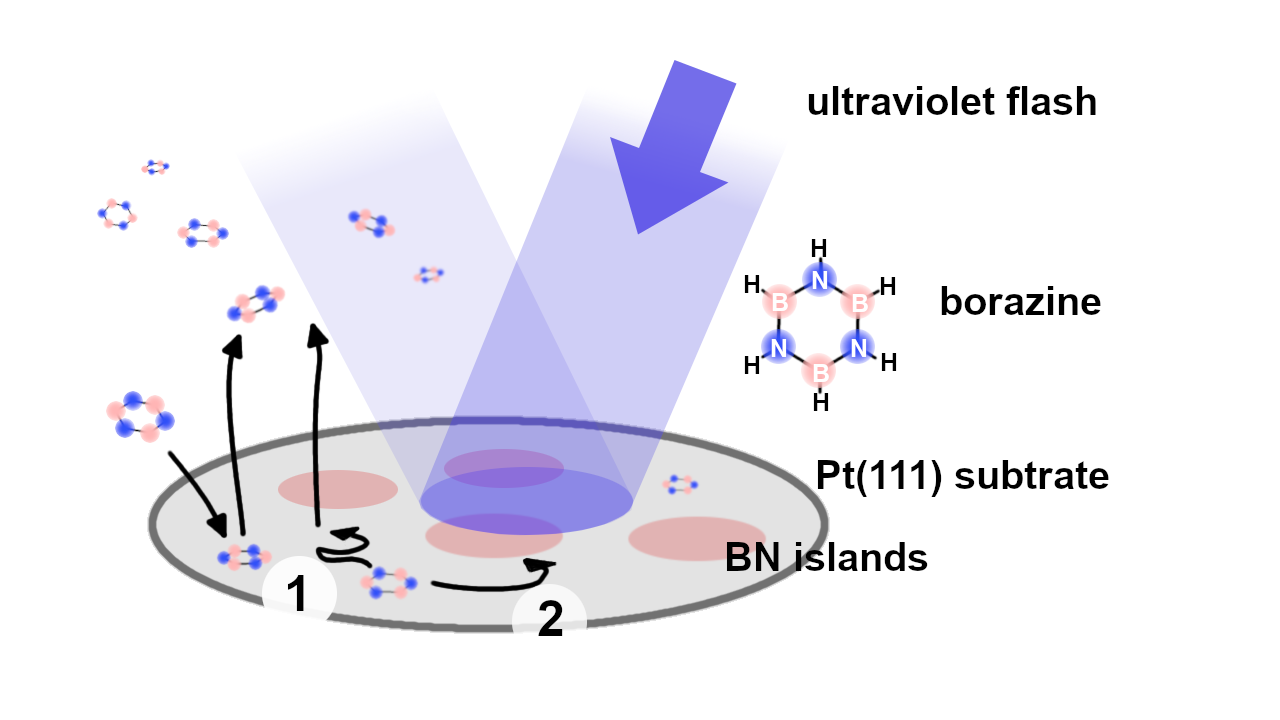
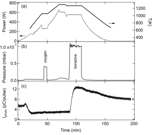
Figure 2 shows a typical 3 hours process-cycle for the production of a monolayer of hexagonal boron nitride on Pt(111). The growth protocol includes temperature, pressure and surface status from photoelectron yield 23. The decrease of the yield upon heating to 700 K indicates desorption of gases from the surface. The final oxygen exposure does not further decrease the yield at 1050 K as it is observed in the first oxygen annealing cycles and marks a clean Pt sample. At this temperature and oxygen pressure the equilibrium oxygen coverage is expected to be low and the work function should not strongly increase 27. The very small increase of the yield upon the O2 exposure at 1050 K may be due to an increased density of single Pt atoms on the surface or due to an increase of the background signal. The significant increase of the photocurrent followed by the admittance of 10-7 mbar (HBNH)3 during 20 minutes at 1273 K illustrates the formation of a -BN layer. The decrease of the yield after preparation is also due to the decrease in sample temperature that has, together with the work function an influence on the photoelectron yield 28. In the following we will analyze the photoelectron yield curve in more detail and show on how much information on the nucleation and growth process may be retrieved.
The electron yield contains contributions from the -BN and the platinum surface portion and a background from photoelectrons of the scattered light . Assuming from the cold walls of the reactor to be constant, knowing the yield of the clean Pt (=0) and the full monolayer (=1) it is straight forward to determine the coverage :
| (1) |
In brackets we note that if shall be determined for different temperatures and for the corresponding temperatures have to be known.
In a picture where the growth rate is proportional to the non-covered surface , the sticking probability and the precursor gas pressure , a first order rate model for the description of the growth of the monolayer () applies:
| (2) |
where is the areal density of BN units in -BN (18.4 nm-2) and the collision current density of the incoming precursor molecules that is proportional to their pressure in the gas phase. For a borazine pressure of 10-7 mbar and room temperature gets 0.17 borazine molecules or 0.51 BN units nm.
Substitution of with and integration of Eq.2 yields with the initial condition :
| (3) |
with the constant being the precursor dose for getting a full monolayer if all incoming molecules would react to -BN: = 2.7 Langmuir, with the mass and the temperature of the precursor gas. The factor applies for borazine that carries 3 BN units.
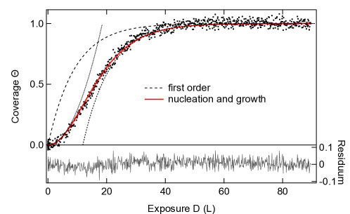
For larger coverages the growth rate slows down as expected from Eq. 3 26, though it misses the correct scaling of the growth onset. Instead of we observe a parabolic onset , which is indicative of nucleation and growth. An ansatz as
| (4) |
provides a parabolic onset of growth. The term models a growth proportional to the perimeter of the -BN nuclei and complies with a picture where adsorbed precursor material may desorb after a certain residence time on the surface. The parameter warrants dimensional homogeneity and accounts e.g. for the nucleation seed geometry and density. Mass conservation asks to be , since the growth rate may not exceed . The validity of Eqn. 4 may be challenged for large coverages, where e.g. percolation of the islands occurs and where the growth rate should not depend on - but over all, the observed kinetics fit well to this equation.
Substitution of with and integration of Eqn. 4 yields with the initial condition the hyperbolic tangent square expression:
| (5) |
It is seen that for small exposures the coverage increases , and approaches full coverage with an exponential like in Eqn. 3, but with an offset. Figure 3 shows the almost perfect fit and the two asymptotes to one data set. The model provides a single parameter =0.3 that characterizes the growth process. At this stage and may not be separated and it is convenient to define the parameter as the effective sticking coefficient. For coverages approaching one we expect all precursor material that sticks on the surface to contribute to the growth, since it reaches the rim of a -BN patch before desorption and this would imply . Analyzing the data sets from different growth temperatures in Figure 4 with an extended model where is not constant but approaches one exponentially, shows to be larger than one for all exposures and that the values of the fits further decrease by about 10 %. Corresponding initial values carry additional information, but here we refrain from refining the model of Eqn. 5.
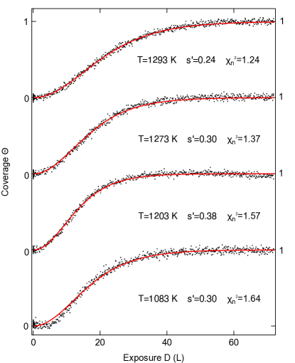
In Figure 4 four subsequent preparations, each starting from clean Pt(111) but at different growth temperatures are shown. It can be seen that is highly non-linear with temperature, and does not decrease monotonously with preparation temperature. This indicates different growth regimes and layer qualities. We furthermore note that the goodness of fit increases with increasing temperature. As a measure for the goodness we use which is the normalized with the number of data points and the standard deviation of single yield measurements before borazine admission. Large indicate a bad fit and a perfect fit is reached with =1.
Comparison of different photoemission yield measurements provides a direct measure for the reproducibility of a process and allows to forecast the expected quality of the grown material. The course of the work function that is derived from the yield is a quality measure that still may be equivocal. For validation it should be correlated with other means of quality control. In the next section we apply the inspection of the crystal-quality after growth by scanning low energy electron diffraction (x-y LEED).
3.2 x-y LEED
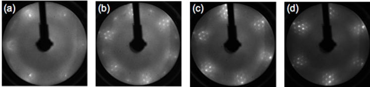
After each preparation where the kinetics are shown in Figure 4 the wafer surface was investigated by LEED before it was cleaned again for the next growth cycle. Figure 5 shows LEED data after the preparations of single layer -BN on Pt(111). The dominant LEED pattern corresponds to an aligned 10 on 9 superstructure 9. At the growth temperatures of T= 1083 K and 1203 K a minority -BN phase that is rotated 30 degrees away from the high symmetry substrate direction is found. This reminds to the earlier study where trichloroborazine was used as a precursor 11. Furthermore, at low temperature a "moiré-ring" with the -BN lattice constant indicates azimuthally disordered -BN. Such moiré-rings were also observed for -BN/Pd(111) 29. However, with increasing preparation temperature the aligned 10 on 9 structure dominates as shown by Preobrajenski et al. 17, 12. In the case of the highest growth temperature of T = 1293 K, rotational misalignment disappeared below the detection limit of our LEED instrument. This indicates that aligned -BN may be grown on Pt(111) with a very high crystal-quality, if the growth is performed at high temperatures.
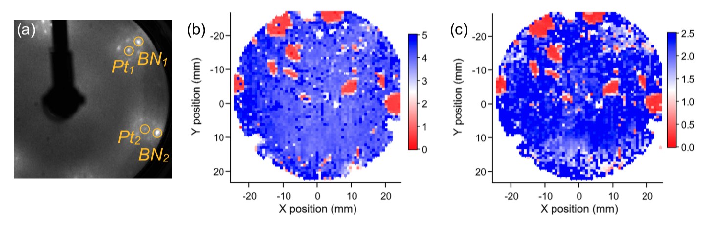
In order to quantify the crystal-quality of the -BN on the wafer scale, the sample was scanned in front of the LEED optics on an x-y piezo motor driven stage. In Figure 6 the results of 4400 sequential LEED measurements for the preparation at 1273 K are shown. The whole wafer displays a 10 on 9 superstructure LEED pattern. From the orientation of the LEED patterns we infer millimeter sized twin-domains. At the electron energy of 100 eV the diffraction patterns from Pt(111) and -BN are three fold symmetric and the pattern of the corresponding twin domain is rotated by 180 degree. Therefore, the intensity ratios of diffraction spots, as indicated in Figure 6(a) are expected to be different for different domains. The intensity ratios in Figure 6(b) indicate a twinning that stems from the substrate growth process. The ratios in Figure 6(c) follow those of the substrate. At the length scale of the experiment (500 m) we find no twinned -BN on a given Pt(111) orientation. For the case of -BN/Ni(111) such and domains have been found 24, while recent -LEED experiments showed as well the formation of and -BN domains on Rh(111) on the micrometer scale 30.
4 Conclusions
We report the observation of the growth kinetics of single layer -BN on 2 inch Pt(111)/sapphire wafers with in-situ photoelectron yield measurements. The coverage vs. exposure curves may be well described with a nucleation and growth model that indicates different effective sticking coefficients for different temperatures. Such growth monitoring data allow an immediate control and improvement of the growth process. After growth the -BN/Pt(111) layers are checked with scanning x-y LEED that reveals the -BN quality and twin-domains in the substrate. The best crystal-quality -BN on Pt(111) is obtained at growth temperatures above 1000 ∘C. {acknowledgement} Financial support by the European Commission under the Graphene Flagship (contract no. CNECT-ICT-604391) is gratefully acknowledged. AH acknowledges a Forschungskredit of the University of Zürich (grant no. FK-20-206 114).
References
- Novoselov et al. 2004 Novoselov, K. S.; Geim, A. K.; Morozov, S. V.; Jiang, D.; Zhang, Y.; Dubonos, S. V.; Grigorieva, I. V.; Firsov, A. A. Electric field effect in atomically thin carbon films. Science 2004, 306, 666–669
- Banszerus et al. 2015 Banszerus, L.; Schmitz, M.; Engels, S.; Dauber, J.; Oellers, M.; Haupt, F.; Watanabe, K.; Taniguchi, T.; Beschoten, B.; Stampfer, C. Ultrahigh-mobility graphene devices from chemical vapor deposition on reusable copper. Sci. Adv. 2015, 1, e1500222
- Tran et al. 2016 Tran, T. T.; Bray, K.; Ford, M. J.; Toth, M.; Aharonovich, I. Quantum emission from hexagonal boron nitride monolayers. Nature Nanotechnology 2016, 11, 37
- Surwade et al. 2015 Surwade, S. P.; Smirnov, S. N.; Vlassiouk, I. V.; Unocic, R. R.; Veith, G. M.; Dai, S.; Mahurin, S. M. Water desalination using nanoporous single-layer graphene. Nat. Nanotechnol. 2015, 10, 459–464
- Cartamil-Bueno et al. 2017 Cartamil-Bueno, S. J.; Cavalieri, M.; Wang, R.; Houri, S.; Hofmann, S.; van der Zant, H. S. J. Mechanical characterization and cleaning of CVD single-layer h-BN resonators. NPJ 2D Mater. Appl. 2017, 1, 1–7
- Mertens et al. 2016 Mertens, S. F. L.; Hemmi, A.; Muff, S.; Groning, O.; De Feyter, S.; Osterwalder, J.; Greber, T. Switching stiction and adhesion of a liquid on a solid. Nature 2016, 534, 676
- Auwärter 2019 Auwärter, W. Hexagonal boron nitride monolayers on metal supports: Versatile templates for atoms, molecules and nanostructures. Surface Science Reports 2019, 74, 1–95
- Zhang et al. 2017 Zhang, K.; Feng, Y.; Wang, F.; Yang, Z.; Wang, J. Two dimensional hexagonal boron nitride (2D-hBN): synthesis, properties and applications. J. Mater. Chem. C 2017, 5, 11992–12022
- Paffett et al. 1990 Paffett, M.; Simonson, R.; Papin, P.; Paine, R. Borazine adsorption and decomposition at Pt(111) and Ru(001) surfaces. Surface Science 1990, 232, 286 – 296
- Auwärter et al. 2004 Auwärter, W.; Suter, H. U.; Sachdev, H.; Greber, T. Synthesis of One Monolayer of Hexagonal Boron Nitride on Ni(111) from B-Trichloroborazine (ClBNH)3. Chemistry of Materials 2004, 16, 343–345
- Muller et al. 2005 Muller, F.; Stowe, K.; Sachdev, H. Symmetry versus commensurability: Epitaxial growth of hexagonal boron nitride on Pt(111) from B-trichloroborazine (ClBNH)(3). Chemistry of Materials 2005, 17, 3464–3467
- Ćavar et al. 2008 Ćavar, E.; Westerström, R.; Mikkelsen, A.; Lundgren, E.; Vinogradov, A.; Ng, M. L.; Preobrajenski, A.; Zakharov, A.; Mårtensson, N. A single h-BN layer on Pt(111). Surface Science 2008, 602, 1722 – 1726
- Gao et al. 2013 Gao, Y.; Ren, W.; Ma, T.; Liu, Z.; Zhang, Y.; Liu, W.; Ma, L.; Ma, X.; Cheng, H.-M. Repeated and controlled growth of monolayer, bilayer and few-Layer hexagonal boron nitride on Pt foils. ACS Nano 2013, 7, 5199–5206
- Laskowski et al. 2008 Laskowski, R.; Blaha, P.; Schwarz, K. Bonding of hexagonal BN to transition metal surfaces: An ab initio density-functional theory study. Phys. Rev. B 2008, 78, 045409
- Grad et al. 2003 Grad, G. B.; Blaha, P.; Schwarz, K.; Auwärter, W.; Greber, T. Density functional theory investigation of the geometric and spintronic structure of h-BN/Ni(111) in view of photoemission and STM experiments. Phys. Rev. B 2003, 68, 085404
- Laskowski and Blaha 2010 Laskowski, R.; Blaha, P. Ab initio study of nanomeshes on Ru(001), Rh(111), and Pt(111). Phys. Rev. B 2010, 81, 075418
- Preobrajenski et al. 2007 Preobrajenski, A. B.; Vinogradov, A. S.; Ng, M. L.; Ćavar, E.; Westerström, R.; Mikkelsen, A.; Lundgren, E.; Mårtensson, N. Influence of chemical interaction at the lattice-mismatched -BNRh(111) and -BNPt(111) interfaces on the overlayer morphology. Phys. Rev. B 2007, 75, 245412
- Goriachko et al. 2007 Goriachko, A.; He,; Knapp, M.; Over, H.; Corso, M.; Brugger, T.; Berner, S.; Osterwalder, J.; Greber, T. Self-Assembly of a hexagonal boron nitride nanomesh on Ru(0001). Langmuir 2007, 23, 2928–2931
- Gsell et al. 2009 Gsell, S.; Fischer, M.; Schreck, M.; Stritzker, B. Epitaxial films of metals from the platinum group (Ir, Rh, Pt and Ru) on YSZ-buffered Si(111). J. Cryst. Growth 2009, 331, 3731–3736
- Hemmi et al. 2014 Hemmi, A.; Bernard, C.; Cun, H. Y.; Roth, S.; Klöckner, M.; Kälin, T.; Weinl, M.; Gsell, S.; Schreck, M.; Osterwalder, J.; Greber, T. High quality single atomic layer deposition of hexagonal boron nitride on single crystalline Rh(111) four-inch wafers. Rev. Sci. Instrum. 2014, 85, 035101
- Lu et al. 2013 Lu, J.; Yeo, P. S. E.; Zheng, Y.; Xu, H.; Gan, C. K.; Sullivan, M. B.; Castro Neto, A.; Loh, K. P. Step Flow Versus Mosaic Film Growth in Hexagonal Boron Nitride. Journal of the American Chemical Society 2013, 135, 2368–2373, PMID: 23327187
- Verguts et al. 2017 Verguts, K.; Schouteden, K.; Wu, C.-H.; Peters, L.; Vrancken, N.; Wu, X.; Li, Z.; Erkens, M.; Porret, C.; Huyghebaert, C.; Van Haesendonck, C.; De Gendt, S.; Brems, S. Controlling Water Intercalation Is Key to a Direct Graphene Transfer. ACS Applied Materials & Interfaces 2017, 9, 37484–37492
- Hemmi et al. 2014 Hemmi, A.; Cun, H.; Roth, S.; Osterwalder, J.; Greber, T. Low cost photoelectron yield setup for surface process monitoring. Journal of Vacuum Science & Technology A 2014, 32, 023202
- Auwärter et al. 2003 Auwärter, W.; Muntwiler, M.; Osterwalder, J.; Greber, T. Defect lines and two-domain structure of hexagonal boron nitride films on Ni(111). Surface Science 2003, 545, L735 – L740
- Dong et al. 2010 Dong, G.; Fourré, E. B.; Tabak, F. C.; Frenken, J. W. M. How Boron Nitride Forms a Regular Nanomesh on Rh(111). Phys. Rev. Lett. 2010, 104, 096102
- Sutter et al. 2011 Sutter, P.; Lahiri, J.; Albrecht, P.; Sutter, E. Chemical Vapor Deposition and Etching of High-Quality Monolayer Hexagonal Boron Nitride Films. ACS Nano 2011, 5, 7303–7309
- Derry and Ross 1985 Derry, G. N.; Ross, P. N. A work function change study of oxygen adsorption on Pt(111) and Pt(100). The Journal of Chemical Physics 1985, 82, 2772–2778
- DuBridge and Hergenrother 1933 DuBridge, L. A.; Hergenrother, R. C. The Effect of Temperature on the Energy Distribution of Photoelectrons. I. Normal Energies. Phys. Rev. 1933, 44, 861–865
- Morscher et al. 2006 Morscher, M.; Corso, M.; Osterwalder, J.; Greber, T. Formation of single layer h-BN on Pd(111). Surf. Sci. 2006, 600, 3280–3284
- Cun et al. 2021 Cun, H.; Miao, Z.; Hemmi, A.; Al-Hamdani, Y.; Iannuzzi, M.; Osterwalder, J.; Altman, M. S.; Greber, T. High-Quality Hexagonal Boron Nitride from 2D Distillation. ACS Nano 2021, 15, 1351–1357, PMID: 33377769