Phase diagram of electron-hole liquid in monolayer heterostructures based on transition metal dichalcogenides
Abstract
In the last few years, interest in monomolecular layers of transition metal dichalcogenides (TMDs) has been driven by their unusual electronic and optical properties, which are very attractive for designing functional elements of new generation nanoelectronics. Recently, experimental evidence has appeared for the formation of a high-temperature strongly bound electron-hole liquid (EHL) in TMD monolayers. Strong binding of charge carriers is due to a significant decrease in the screening of the Coulomb interaction in monolayer heterostructures. In this work, the gas–liquid phase transition in a system of electrons and holes in quasi-two-dimensional heterostructures based on TMDs is considered and the critical parameters of such a transition are calculated. The metal-insulator transition is described and the phase diagram for such heterostructures is constructed.
pacs:
71.35.−y, 73.21.Fg, 73.90.+fI Introduction
The last fifteen years have been marked by intensive research of two-dimensional (2D) carbon material, graphene, as the basis for new generation nanoelectronics RS2018 . Extensive activities have arisen to study 2D materials such as monolayers of hexagonal boron nitride, black phosphorus, transition metal dichalcogenides (TMDs), and many other compounds Miro2014 . A promising direction of this activity has become the creation and study of vertical (van der Waals) heterostructures, in which various 2D materials are combined in a given sequence Geim2013 .
Monomolecular layers of TMDs fill a special place in the current studies of 2D materials. They have the structure of a sandwich with a layer of transition metal atoms , enclosed between layers of chalcogen atoms , and are described by the chemical formula . The most studied representatives of this class of substances are compounds with metal atoms of group VI ( = Mo, W) and S, Se, Te as a chalcogen. Bulk layered TMDs, such as MoS2, WS2, MoSe2, WSe2, have an indirect bandgap eV Bulaevskii1975 ; Bulaevskii1976 , and their monomolecular layers become direct-gap semiconductors with about 2 eV Durnev2018 .
In TMD monolayers, it is possible to achieve valley-selective excitation of charge carriers by a circularly polarized electromagnetic wave Zeng ; Mak1 ; XiaoD ; CaoT ; Jones . This prompted researchers to develop a new type of nanoelectronic devices, valleytronics, where a selective transfer of charge carriers with a certain valley index would take place RS2018 ; WangQH ; Mak2 ; Mak3 .
The optical properties of monomolecular layers of TMDs are largely determined by excitons and trions. The binding energy of the exciton in TMD is hundreds of meV, and of the trion is tens of meV Durnev2018 . The inclusion of thin TMD layers in van der Waals heterostructures makes it possible to observe many-particle effects in systems with long carrier lifetime. Due to these factors, TMD-based structures are considered perfect systems for studying high-temperature electron-hole liquid (EHL).
Usually, energy of one electron-hole (-) pair in EHL is , and the critical temperature of the gas–liquid phase transition is Andryushin1977a ; Rice1980 ; JeffrisKeldysh1988 ; Tikhodeev1985 ; Sibeldin2016 ; Sibeldin2017 . Therefore, it can be expected that EHL will be observed in monolayers of TMDs even at room temperatures.
A number of papers were published in 2019 on EHL in monolayers of TMDs. Let’s dwell on them in more detail to highlight the current situation.
Note the paper Bataller2019 , which presents the results of observation of electron-hole plasma (EHP) in the MoS2 monolayer. Although EHL was not observed, the obtained results are important for further research. In particular, it was demonstrated that photoexcitation of a MoS2 monolayer leads to a direct–indirect bandgap transition, which favors the EHL formation.
It was shown in Younts2019 that an increase in the intensity of continuous optical excitation of a MoS2 monolayer in the below-gap regime initiates the transition of an insulator exciton gas into a metallic EHP.
A high-temperature strongly coupled EHL with K in a suspended monolayer MoS2 was investigated in the work Yu2019 . A first-order gas–liquid phase transition was observed. With the same excitation, EHL differs from EHP by a higher charge carrier density and, hence, by a higher photoluminescence. In the experiment, a sharp step-like increase in photoluminescence was observed when the pump power increased to kW/cm2. The EHL incompressibility was demonstrated: with a further increase in the pump power, the area occupied by EHL increased in proportion to the number of generated - pairs, while the EHL density remained constant. Authors of the work Yu2019 have observed the appearance of a luminescent ring caused by a phonon wind (see, e.g., the review Tikhodeev1985 and the references cited therein).
EHL was studied at room temperature in ultrathin photocells graphene–a thin (several monolayers) MoTe2 film–graphene Arp2019 . When the power of the exciting laser reached mW, the - pair density became so large that the average distance between them nm was comparable to the Bohr radius of excitons nm Sun2017 . Under these conditions, the exciton annihilation (the transition of an insulator exciton gas into a metallic EHP) was observed. Then, at a higher value of the laser power mW, EHP underwent a gas–liquid transition. The formation of a 2D EHL droplet was proved by the appearance of a characteristic dependence for the photocurrent on the exciting laser power and the photocurrent dynamics on a picosecond scale. A similar behavior was observed during the formation of EHL droplets in traditional semiconductors (Si, Ge, GaAs, etc.) at low temperatures Rice1980 ; JeffrisKeldysh1988 .
The theoretical work Rustagi2018 is devoted to the calculation of the EHL phase diagram in a suspended monolayer MoS2. The work was motivated by the experimental results outlined in the paper Yu2019 . To calculate the EHL properties, the authors of Rustagi2018 used a potential describing the Coulomb interaction of charge carriers in films of finite thickness (the Keldysh potential Rytova1967 ; Chaplik1971 ; Keldysh1979 ), which has proven itself well to explain the significant deviation of the energy of several first exciton levels from the Rydberg series Durnev2018 .
According to Rustagi2018 estimates, the metal–insulator transition in MoS2 occurs in the liquid phase at a density higher than the critical value for the gas–liquid transition. Note that EHP in an ultrathin MoTe2 film is in many respects similar to EHP in the MoS2 monolayer. Therefore, most likely, the metal–insulator transition precedes the gas–liquid transition in both systems.
In our opinion, such a qualitative discrepancy is caused by the unjustified use of the Keldysh potential in the EHL calculations Rustagi2018 , which leads to a shift of the critical point towards lower densities and temperatures. When calculating the exciton and EHL, the main contributions come from substantially different perturbation theory diagrams, ladder and loop diagrams, respectively.
The influence of the dielectric environment, as well as electron doping (when the densities of electrons and holes are not equal) on the EHL phase diagram (gas–liquid and metal–insulator transitions) were investigated in Steinhoff2017 by the method of spectral functions. The EHL phase diagram in doped multi-valley semiconductors was considered earlier in the works Andryushin1990a ; Andryushin1991 ; Andryushin1990b .
We showed in our previous work Pekh2020 that the formation of a high-temperature strongly compressed and strongly coupled EHL in monolayer heterostructures based on TMDs is due to the weakening of the Coulomb interaction screening. The Coulomb interaction of charge carriers in monolayer films is determined by the half-sum of permittivities of the environment (for a sample on a substrate, this is a vacuum and a substrate, and for a suspended sample, this is a vacuum). In both cases, the effective permittivity is significantly lower than that of TMD films. As a result, EHL is formed with an anomalously high ground state energy , which is fractions of eV, and a high density . For example, experimental values for a suspended monolayer MoS2 are eV and cm-2 Younts2019 .
Based on our previous results, in this paper we investigate the EHL phase diagram in quasi-2D TMD-based heterostructures.
EHL appears through a first-order phase transition, when the density of free and/or bound carriers in excitons reaches a certain temperature-dependent critical value of the saturated vapor density Andryushin1977a . At the critical temperature , the critical - pair density is reached.
In this work, we investigate the metal–insulator transition (Mott transition), which occurs at the - pair density . With increasing density, this transition usually precedes the gas–liquid transition () and is in the gas phase Andryushin1977a ; Rice1980 .
We will search for semiconductors in whose films EHL will be characterized by the highest binding energy and, therefore, the highest critical temperature. For this, we will consider model semiconductors with different numbers of electron and hole valleys and unequal effective masses of electrons and holes.
II Model foundations
We describe a model quasi-2D nonequilibrium - system by the Hamiltonian Andryushin1976a ; Andryushin1976b
| (1) |
Here () and () are Fermi operators of annihilation (creation) of an electron and a hole with quasimomentum and spin in the valleys and , respectively. The number of electron valleys is , and the number of hole valleys is . In general case, .
The normalized area of the layer is set equal to one. We use a system of units with Planck’s constant and twice the reduced mass is (). In this work, along with the ratio of the effective masses of the electron and hole , we use the parameter .
To take into account the interaction in EHL, we use here the usual 2D Coulomb potential , rather than the Keldysh potential Rustagi2018 ; Rytova1967 ; Chaplik1971 ; Keldysh1979 ; Pekh2020
| (2) |
where the “screening length” , is the film thickness, , is the permittivity of the film material, is the effective permittivity of the media surrounding the film (e.g., for vacuum and for the SiO2 substrate). As applied to TMD monolayer systems, the quantity is an adjustable parameter in the exciton calculations Durnev2018 .
In the previous work Pekh2020 , we showed that the use of the Keldysh potential for calculating EHL is not justified. With the help of one adjustable parameter, it is impossible to agree both calculated characteristics with the experimental ones: the binding energy of EHL and its equilibrium density.
We also put , when defining the system of units. Then, the binding energy and the radius of the 2D exciton are automatically equal to unity: and . Below, it is assumed that the energy and temperature are measured in , and the - pair density are measured in .
In the next two sections, we will focus on the calculation of the ground state energy of EHL and its thermodynamics in the TMD monolayer, using, among other things, the previously obtained results for quasi-2D systems Klyuchnik1978 ; Andryushin1979 ; Silin1988 .
III Ground state energy
We are considering a semiconductor in which the number of electron and hole valleys is not necessarily equal. In what follows, without loss of generality, we will assume that (i.e., we call charge carriers with the largest number of valleys electrons). The momenta will be measured in units of , where and are the Fermi momenta of electrons and holes, respectively, ( is the 2D charge carrier density). Frequency will be measured in units of . We introduce the dimensionless distance between the particles .
Hereinafter, we assume that there is spin degeneracy for both electrons and holes.
In some cases, the spin-orbit splitting of the valence band in TMD is very large (e.g., in MoS2 it is equal to 148 meV Rustagi2018 ), then should be used instead of .
We also recall that under intense photoexcitation of the MoTe2 film, holes flow down to the point and , while the number of electron valleys does not change and Arp2019 .
The ground state energy of 2D EHL per one - pair is
| (3) |
The first term is the kinetic energy ( and )
| (4) |
The second term is the exchange energy
| (5) |
The third term is the correlation energy, which we represent as an integral over the momentum transfer Pekh2020 ; Combescot1972 ; Andryushin1976a ; Andryushin1976b ; Andryushin1977b
| (6) |
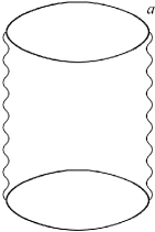
For , we use the random phase approximation (RPA) Combescot1972 ; Andryushin1976a ; Andryushin1976b ; Andryushin1977b . The function for is determined by the sum of diagrams of the second order in the interaction (Fig. 1). In the intermediate region, the function is approximated by a segment of the tangent Pekh2020 ; Andryushin1976a ; Andryushin1976b .
For arbitrary values of and , the expansion of the function for small turns out to be rather cumbersome. For the case of equal masses of an electron and a hole () and an equal number of electron and hole valleys (), it is given in our previous work Pekh2020 .
The terms in at with half-integer powers of are the contribution from the 2D plasmon
| (7) |
Here, and .
It is interesting to note that, in contrast to the three-dimensional (3D) case, in the 2D case there is also a branch of damped excitations
| (8) |
When the inequalities
| (9) |
are satisfied, two branches of damped oscillations are also possible
| (10) |
| (11) |
We assumed that the most frequent case is realized (for many TMDs and for the relation ).
The inequalities (9) are satisfied for ,
| (12) |
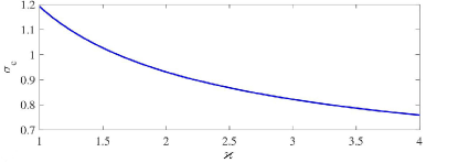
In particular, . The graph of the function is shown in Fig. 2.
Apparently, the presence of additional branches (8), (10), (11), which are absent in the 3D case, provides 2D EHL binding.
The EHL equilibrium energy is the minimum of the ground state energy
where is the equilibrium EHL density.
The equation for
is very cumbersome and for the sake of brevity we do not present it here. In the case of an equal number of electron and hole valleys, to determine and , one can use, respectively, formulas (21) and (22) of our work Pekh2020 .
IV Monolayer thermodynamics
In keeping with the analogy of nonequilibrium charge carriers in semiconductors with electrons and ions in crystals, L. V. Keldysh suggested Keldysh1968 that with a decrease in temperature or an increase in the density of excitons or exciton molecules (biexcitons), this gas will be liquefied into EHL and the system will undergo a first-order gas–liquid phase transition. Since the late 1960s, the EHL formation has been observed in many semiconductors (see, e.g., Rice1980 ; JeffrisKeldysh1988 ; Tikhodeev1985 ; Sibeldin2016 ; Sibeldin2017 and references therein).
The gas–liquid transition corresponds to a bell-shaped curve on the plane with a critical point in the top. This curve passes through the points and at . The value of is determined by the equality , where is the biexciton dissociation energy JeffrisKeldysh1988 . The region to the left of the branch emerging from the point corresponds to a (bi)exciton insulator gas; to the right of the branch , emerging from the point , there is an EHL region. Under the “bell” there is an unstable region in which separation into EHL droplets with a density and a saturated vapor of excitons or - pairs with a density occurs.
The phase diagram also contains a second bell-shaped curve, which corresponds to the exciton–plasma transition (metal–insulator transition). The construction of this curve for arbitrary densities and temperatures is difficult and we restrict ourselves to estimates in the most interesting areas. In the classical region (, is the Fermi energy of - pairs), this curve is determined by the reaction of exciton formation from a free electron and a free hole. As the density increases at a given temperature, electrons and holes are bound to form excitons. In the quantum region (), an increase in the density of excitons leads to their dissociation (a Mott transition occurs). The possibility of a metal–insulator transition in the liquid phase was discussed in the works Bisti1978 ; Lobaev1984 .
In the region , excitons undergo thermal dissociation. Therefore, the transition of excitons to EHP is significantly smeared out and the exciton spectra at approaching have a diffuse character Kukushkin1983 .
The most promising for the observation of the exciton–plasma transition are semiconductors, in which the EHL stability decreases and decreases due to the lifting of the band degeneracy. Due to this, in such semiconductors at sufficiently low temperatures, it is possible to realize excitonic gas densities close to . For example, it was experimentally found in uniaxially deformed Ge that the metal–insulator transition occurs at . This is in good agreement with the estimate obtained using dielectric screening of excitons Bisti1978 .
The three-component system (EHL, free excitons, and free charge carriers) was considered in the works Keldysh1974 ; Sanina1985 .
Calculations of the thermodynamic properties of EHL in quasi-2D systems were carried out earlier in works Klyuchnik1978 ; Andryushin1979 ; Silin1988 . Materials such as TMD monolayers and graphene are 2D crystals. The thermodynamics of - systems is equally applicable to both quasi-2D heterostructures and 2D crystals. However, for the latter, there is a doubt about their stability with respect to vibrations of atoms across the plane of the crystal Lozovik2008 . In addition, in the process of intense photoexcitation, local overheating of the sample can occur. This can lead to a local deformation of the crystal lattice and to melting of 2D crystal Berezinskii1970 ; Berezinskii1971 ; KostelitzThouless1973 ; NelsonHalperin1978 ; NelsonHalperin1979 . The experimentally observed intense photoluminescence allows us to conclude that there are almost no defects in TMD monolayers. Nonradiative recombination of charge carriers at defects would lead to luminescence quenching. We believe that the melting temperature significantly exceeds the critical temperature of the gas–liquid transition , and intense photoexcitation of 2D crystal can only lead to the lifting of the valley degeneracy, which was observed, for example, in an ultrathin film MoTe2 Arp2019 .
We represent the chemical potential of an - pair ensemble in a TMD monolayer in the form Andryushin1979 ; Silin1988
| (13) |
The right-hand side of (13) is the chemical potential of noninteracting particles (first term) together with exchange and correlation contributions (second and third terms, respectively). We have neglected in (13) the dependence of and on temperature, since the temperature corrections to and cancel each other at . This is in agreement with the previously obtained results for the 3D case JeffrisKeldysh1988 ; Thomas1974 ; Rice1974 .
The critical point of the gas–liquid transition is determined by two equations
| (14) |
To test our methods for studying the EHL phase diagram in TMD monolayers, we calculated the similarity relation typical for the gas–liquid transition in general (see the note on p. 262 of the book Landau5 ) Andryushin1977a , as well as the ratio of the critical density to the equilibrium one JeffrisKeldysh1988 .
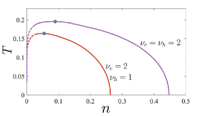
Table 1 shows the results of the numerical solution of the equations (14) for . Note that for a relatively small number of valleys, the ratio is almost independent of the number of valleys. The maximum of this ratio is attained for the system , which is possible for alloys of the form MoxW1-xS2 with equivalent energy valleys MoS2 and WS2.
| (1, 1) | (2, 1) | (2, 2) | (4, 1) | (4, 4) | |
|---|---|---|---|---|---|
| 0.035 | 0.054 | 0.089 | 0.075 | 0.242 | |
| 0.136 | 0.164 | 0.196 | 0.198 | 0.294 | |
| 0.164 | 0.264 | 0.450 | 0.394 | 1.302 | |
| 1.090 | 1.340 | 1.661 | 1.606 | 2.545 | |
| 4.686 | 4.889 | 5.056 | 5.253 | 5.379 | |
| 8.015 | 8.171 | 8.111 | 8.070 | 8.718 |
The results of the numerical calculation of the ratios and for a different number of valleys are shown in Fig. 3.
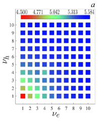
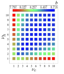
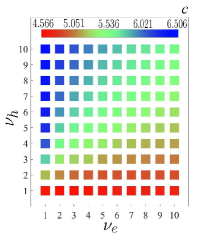
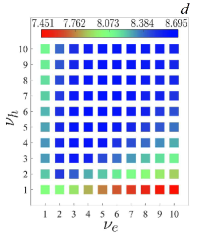
For , the area (the upper right corner on the upper panels of Fig. 3) corresponds to close to maximum and .
For or for is close to the maximum, and tends to the minimum. This is due to the faster growth of compared to in these areas.
At (here is taken, see the bottom left panel of Fig. 3) changes noticeably: the minimum moves to the region with large and small ; the maxima remain in the region of large and small ; for , the values are intermediate. It is interesting to note that there is no such restructuring for the more fundamental relation , and changes occur mainly in the region (see lower right panel Fig. 3).
In the limit of a large number of valleys (), the correlation energy in the expression (13) is a power density function
| (15) |
For 2D systems, the exponent is . The function was defined by us in the previous work Pekh2020 . In particular, .
In the limit , the exchange contribution to both the energy and the chemical potential can be neglected. In this case, the pair of equations (14) is reduced Andryushin1977a to the equation
| (16) |
with variable . Here, .
The critical parameters of the EHL are expressed in terms of by the formulas
| (17) |
| (18) |
| (19) |
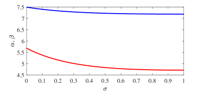
Note that in the limit the relations and do not depend on
| (20) |
| (21) |
and weakly depend on (see Fig. 4).
In the particular case , the equation (16) is greatly simplified:
| (22) |
For it has the solution , while and ,
| (23) |
| (24) |
| (25) |
The function is obtained with good accuracy by expanding the right-hand side of (16) in a series in up to terms of the third order:
| (26) |
then
| (27) |
| (28) |
| (29) |
To obtain the temperature dependence of the - pair density in the gas and liquid phases, we use the Maxwell rule
| (30) |
where .
The set of pairs of points and forms a bell-shaped curve in the plane . Two typical curves for a TMD monolayer with and and in the case of are shown in Fig. 5.
For , we find, with the same accuracy as (26), the temperature dependences of the - pair density in the gas and liquid phases and the chemical potential near the critical point
| (31) |
| (32) |
At low temperatures , the density in the gas phase is exponentially small
| (33) |
where . In the liquid phase, it deviates from the equilibrium EHL density quadratically in temperature
| (34) |
The chemical potential correction is also quadratic in temperature
| (35) |
The formulas (16)–(22) and (26)–(35) were written by us for an arbitrary with the purpose that we will need these formulas when considering 3D layered systems, when . The corresponding formulas are given in the work Andryushin1977a .
A TMD monolayer, generally speaking, is a “three-layer” system in which a layer of transition metal atoms is inserted between two layers of chalcogen atoms. Therefore, it may turn out that the relevant value of the exponent in the correlation energy will be intermediate between and .
In the case of a finite number of valleys, one can choose the effective exponent in the expression for the correlation energy (15) so that simple approximate calculations agree with the exact ones. For this, two criteria can be proposed: 1) by the coincidence of with that obtained from the equation (20); 2) by coincidence of with that obtained from the equation (21).
Based on the data in Table 1, we calculated for the case the effective values of and by both criteria: and by the first criterion, and by the second criterion (see Table 2).
| (1, 1) | (2, 1) | (2, 2) | (4, 1) | (4, 4) | |
|---|---|---|---|---|---|
| 0.341 | 0.320 | 0.305 | 0.291 | 0.281 | |
| 0.300 | 0.296 | 0.285 | 0.299 | 0.280 | |
| 2.976 | 3.006 | 3.021 | 3.121 | 3.313 | |
| 2.763 | 2.910 | 2.974 | 3.143 | 3.314 |
The case of finite can be very different from the limiting case of . In a single-valley semiconductor, when the formula (15) for the correlation energy is unlikely to work, . The coincidence of and improves as the number of valleys increases. For the number of valleys is large enough and and the question of choosing a criterion is insignificant. In this case, the effective exponent is closer to the layered than to , indicating an analogy between multi-valley and multi-layer systems.
In the case of a small number (one or two electron (hole) valleys), one should decide on the choice of the criterion. Numerical calculations of phase diagrams for systems with , , and using the expression (15) showed better agreement with the curves calculated earlier (see Fig. 5) for the effective exponent . Thus, in our opinion, the second criterion is more accurate.
The results obtained for the effective exponent can be used to calculate the exchange-correlation contribution in the density functional method Kryachko2014 ; Jones2015 ; Bretonnet2017 ; InTech2019 .
V Metal–insulator transition in monolayer
In the introduction, we pointed out a qualitative discrepancy between the theoretical work Rustagi2018 and the experiment Arp2019 . In the experiment, with increasing excitation, the metal–insulator transition preceded the gas–liquid transition, i.e. the metal–insulator transition occurred in the gas phase, and theoretical calculations predicted that this transition occurs in the liquid phase. We noted that the indicated discrepancy arose due to the unjustified use of the Keldysh potential in calculating the EHL ground state energy.
The authors of the work Rustagi2018 took as a criterion for the occurrence of a metal–insulator transition the equality , where is the bandgap renormalization, ( is the bare value of the bandgap), . Qualitatively, this corresponds to the “creeping” of the bottom of the conduction band with an increase in the - pair density to the exciton level, if its position is assumed to be unchanged. In our opinion, this criterion is incorrect because it does not take into account the screening of the Coulomb interaction at a high - pair density. We are “approaching” the metal–insulator transition from the side of low densities. The renormalization of the bandgap in this density range can be neglected, because the density of free - pairs in the insulator (exciton) phase is low.
We use vanishing the ground state energy (binding energy) of the exciton as a criterion for the metal–insulator transition
| (36) |
Here, is the density of this transition.
To find the dependence , we solve by the variational method the Schrödinger equation in the momentum representation
| (37) |
( is the reduced mass of an electron and a hole).
Screened Coulomb potential at a high - pair density Andryushin1979 ; Silin1988 ; Andryushin1981
| (38) |
where the initial unscreened Coulomb interaction is taken in the form of the Keldysh potential (2), is static 2D polarization operator of electrons and holes
| (39) |
Here, is the Heaviside function,
The polarization operator is taken in the static limit, since we are interested in vanishing the exciton binding energy. differs from that used in the works Andryushin1979 ; Andryushin1981 in that the expression for takes into account the presence of several valleys ( electron and hole ones).
The function is the Hubbard correction to RPA taking into account the contribution of the exchange diagrams at high momentum transfers Andryushin1979 ; Andryushin1981 ; Hubbard1957 . In the case of an equal number of valleys
| (40) |
Here, it is taken into account that the number of the exchange diagrams grows linearly in , while the number of the loop diagrams grows quadratically in . Therefore, the relative contribution of the former decreases as .
In the case of , the Fermi momenta of electrons and holes are different and it is convenient to take their geometric mean , then
| (41) |
The trial wave function is chosen in the form of the Fourier transform of an exponentially decreasing wave function of 2D exciton ( is the variational parameter)
| (42) |
We checked the correctness of the variational calculations for the case of zero charge carrier density (). Table 3 summarizes the calculated and experimental data on the exciton binding energy for eight heterostructures.
| Heterostructure | () | (Å) | (meV) | (meV) | References | |
|---|---|---|---|---|---|---|
| MoS2/SiO2 | 0.3200.04 | 16.926 | 2.45 | 336 | 31040 | Eknapakul2014 ; Berkelbach2013 ; Rigosi2016 |
| BN/MoS2/BN | 0.2750.015 | 7.640 | 4.45 | 215 | 2213 | Goryca2019 |
| BN/MoSe2/BN | 0.3500.015 | 8.864 | 4.4 | 226 | 2313 | Goryca2019 |
| BN/MoTe2/BN | 0.3600.04 | 14.546 | 4.4 | 173 | 1773 | Goryca2019 |
| WS2/SiO2 | 0.220 | 15.464 | 2.45 | 310 | 36060 | Berkelbach2013 ; Rigosi2016 ; Rasmussen2015 |
| BN/WS2/BN | 0.1750.007 | 7.816 | 4.35 | 175 | 1803 | Goryca2019 |
| WSe2/SiO2 | 0.230 | 18.414 | 2.45 | 283 | 370 | Berkelbach2013 ; Rasmussen2015 ; He2014 |
| BN/WSe2/BN | 0.2000.01 | 10 | 4.5 | 158 | 1673 | Goryca2019 |
To calculate the exciton binding energy in a MoS2 monolayer on a SiO2 substrate (MoS2/SiO2), the effective electron and hole masses were taken from the experiment Eknapakul2014 . The value of the screening length was taken from the theoretical work Berkelbach2013 . Our result was compared with the experimental exciton binding energy Rigosi2016 . A close value of the binding energy (340 meV) was obtained by the variational solution of the Schrödinger equation in the coordinate space Ratnikov2020 .
For TMD monolayers encapsulated by thin layers of hexagonal boron nitride (BN), the experimental data were taken from Goryca2019 .
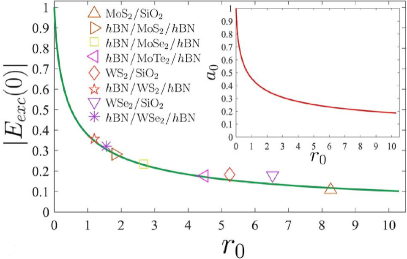
For WS2 and WSe2 on a SiO2 substrate (WS2/SiO2 and WSe2/SiO2), the calculated parameters were taken from the works Berkelbach2013 ; Rasmussen2015 . The experimental exciton binding energies in WS2/SiO2 and WSe2/SiO2 were obtained, respectively, in the works Rigosi2016 and He2014 .
For the MoS2/SiO2 and WS2/SiO2 heterostructures, calculated by us binding energies fall within the experimental error ranges. For other heterostructures, the calculated values are also in good agreement with the experimental ones, with the exception of WSe2/SiO2, for which the error range was not given He2014 . As can be seen from Table 3, on the whole, good agreement between our calculations and experiment was achieved.
We also calculated the dependence of the binding energy on (see Fig. 6). It should be noted that the error ranges for the dimensionless experimental values of the binding energy also appeared along the abscissa axis, since the unit of measurement , by which we nondimensionalized , has an error caused by inaccuracy in measuring the effective masses of charge carriers. For the same reason, inaccuracies in also introduce an additional error into the dimensionless value . The experimental points for all heterostructures (except for WSe2/SiO2), taking into account the errors, coincide with the calculated curve. For the WSe2/SiO2 heterostructure, the authors of He2014 apparently calculated the exciton binding energy for a suspended sample in vacuum, which gave an overestimated value of .
We come to the conclusion that the method described above for the variational solution of the Schrödinger equation is applicable to finding the exciton binding energy at zero - pair density.
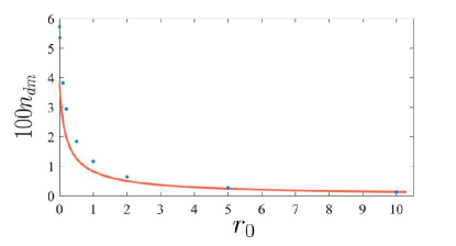
We have investigated the dependences of the metal–insulator transition density at zero temperature on the screening length for various numbers of electron and hole valleys and the ratio of the charge carrier masses (). The resulting curves for different and turned out to be very close. We compared the results of our calculations for with those published in Andryushin1981 for (see Fig. 7). In the region of interest to us, , the values of are also very close to the calculated curve. This allows us to conclude that is weakly dependent on , , and .
To calculate the dependence of the exciton binding energy on the - pair density at , we need a polarization operator at a finite temperature. After summation over discrete Matsubara frequencies and analytic continuation to real frequencies, we find its real part at zero frequency in the form
| (43) |
| (44) |
where is the Fermi distribution function of the th kind particles () with the chemical potential (calculated for a gas of non-interacting particles), is the dispersion law of the th kind particles (plus for electrons, minus for holes). The bar near the integral means that it is taken in the sense of the principal value.
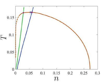
Using the values of , , and given in Table 3, we calculated the temperature dependences of the metal–insulator transition density for MoS2/SiO2 and BN/MoS2/BN heterostructures and compared them with the gas–liquid transition curve in Fig. 8. Points of intersection of curves on the phase diagram are (2.8 cm-2) at (638 K) for the first heterostructure and (4.6 cm-2) at (412 K) for the second heterostructure. The critical point of the gas–liquid transition (5.5 cm-2 and 4.2 cm-2 for the first and the second heterostructures, respectively) and (644 K and 412 K for the first and second heterostructures, respectively) is between them. Consequently, in MoS2/SiO2 the transition is in the gas phase, and in BN/MoS2/BN the transition is in the liquid phase.
Note that the and values for the BN/MoS2/BN heterostructure are very close (the difference is %) and we cannot strictly assert that the transition occurs in the liquid phase. Refinement of calculations of using dielectric screening Lobaev1984 will be carried out by us in the next work.
VI Conclusion
In this work, we calculated the EHL phase diagram in monolayer heterostructures based on TMD for an arbitrary ratio of the electron and hole masses and the number of valleys.
We have demonstrated that in the multivalley case, the main contribution to the EHL formation is the correlation energy. We showed that the EHL binding energy and the EHL equilibrium density increase with the number of valleys in TMD. Note that for the same total number of valleys, the maximum values are achieved with the equal number of electron and hole valleys.
We have shown that the relationship between the critical temperature of the gas–liquid transition and the EHL binding energy is satisfied with good accuracy for various heterostructures.
The method developed by us made it possible to determine the power law of the dependence of the correlation energy on the density and to estimate the exponent . Calculations have shown that it is limited to values for 3D (layered or multi-valley) and 2D cases, respectively, . An exception are single-valley TMDs, for which the power law for the correlation energy is inapplicable due to the absence of a small parameter.
We investigated the dependence of the exciton binding energy in monolayer TMD-based heterostructures on their parameters and found good agreement between the calculated and experimental values.
We studied the metal–insulator transition. As a criterion for such a transition, we used vanishing the exciton binding energy with an increase in the charge carrier density. The corresponding density weakly depends on the number of valleys and the ratio of the electron and hole masses.
Usually, the metal–insulator transition is in the gas phase. We have shown that the dielectric environment of a TMD monolayer can determine in which phase (gas or liquid) the transition from the insulator to the metallic phase occurs. An example of such behavior are heterostructures based on the MoS2 monolayer. If the monolayer is on a SiO2 substrate, then the metal–insulator transition occurs in the gas phase, and if the monolayer is encapsulated by BN, then the transition, apparently, occurs in the liquid phase. It should be noted that the point of the metal–insulator transition is very close to the critical point of the gas–liquid transition in an encapsulated monolayer and the obtained results are not very reliable and require refinement.
In our opinion, heterostructures based on a MoS2 monolayer, freely suspended or located on a SiO2 substrate, are the most interesting for studying EHL and the metal–insulator transition, since it has maximum and .
It is interesting to investigate how the external dielectric environment and electron doping affect the metal–insulator transition and to find out in which phase (gas or liquid) it occurs.
Acknowledgements.
P. V. Ratnikov thanks for financial support the Foundation for the Advancement of Theoretical Physics and Mathematics “BASIS” (the project no. 20-1-3-68-1).References
- (1) P. V. Ratnikov and A. P. Silin, Phys. Usp. 61, 1139 (2018).
- (2) P. Miró, M. Audiffred, and T. Heine, Chem. Soc. Rev. 43, 6537 (2014).
- (3) A. K. Geim and I. V. Grigorieva, Nature 499, 419 (2013).
- (4) L. N. Bulaevskiĭ, Sov. Phys. Usp. 18, 514 (1975).
- (5) L. N. Bulaevskiĭ, Sov. Phys. Usp. 19, 836 (1976).
- (6) M. V. Durnev and M. M. Glazov, Phys. Usp. 61, 825 (2018).
- (7) H. Zeng, J. Dai, W. Yao et al., Nature Nanotechnol. 7, 490 (2012).
- (8) K. F. Mak, K. He, J. Shan, and T. F. Heinz, Nature Nanotechnol. 7, 494 (2012).
- (9) D. Xiao, G.-B. Liu, W. Feng et al., Phys. Rev. Lett. 108, 196802 (2012).
- (10) T. Cao, G. Wang, W. Han et al., Nature Commun. 3, 887 (2012).
- (11) A. M. Jones, H. Yu, N. J. Ghimire et al., Nature Nanotechnol. 8, 634 (2013).
- (12) Q. H. Wang, K. Kalantar-Zadeh, A. Kis et al., Nature Nanotechnol. 7, 699 (2012).
- (13) K. F. Mak, K. L. McGill, J. Park, and P. L. McEuen, Science 344, 1489 (2014).
- (14) K. F. Mak and J. Shan, Nature Photon. 10, 216 (2016).
- (15) E. A. Andryushin, L. V. Keldysh, and A. P. Silin, Sov. Phys. JETP 46, 616 (1977).
- (16) T. M. Rice, Solid State Phys. 32, 1 (1978); J. C. Hensel, T. G. Phillips, G. A. Thomas, ibid., 87 (1978).
- (17) Electron–Hole Droplets in Semiconductors, Ed. by C. D. Jeffries and L. V. Keldysh (Elsevier Science, Amsterdam, 1983).
- (18) S. G. Tikhodeev, Sov. Phys. Usp. 28, 1 (1985).
- (19) N. N. Sibeldin, JETP 122, 587 (2016).
- (20) N. N. Sibeldin, Phys. Usp. 60, 1147 (2017).
- (21) A. W. Bataller, R. Younts, A. Rustagi et al., Nano Lett. 19, 1104 (2019).
- (22) R. Younts, A. Bataller, H. Ardekani et al., Phys. Status Solidi B 256, 1900223 (2019).
- (23) Y. Yu, A. W. Bataller, R. Younts et al., ACS Nano 13, 10351 (2019).
- (24) T. B. Arp, D. Pleskot, V. Aji, and N. M. Gabor, Nature Photon. 13, 245 (2019).
- (25) Y. Sun, J. Zhang, Z. Ma et al., Appl. Phys. Lett. 110, 102102 (2017).
- (26) A. Rustagi and A. F. Kemper, Nano Lett. 18, 455 (2018).
- (27) N. S. Rytova, Moscow University Physics Bulletin 22, (3), 18 (1967).
- (28) A. V. Chaplik and M. V. Entin, Sov. Phys. JETP 34, 1335 (1972).
- (29) L. V. Keldysh, JETP Lett. 29, 658 (1979).
- (30) A. Steinhoff, M. Florian, M. Rösner et al., Nature Comm. 8, 1166 (2017).
- (31) E. A. Andryushin and A. P. Silin, Sov. Phys. Solid State 32, 1746 (1990).
- (32) E. A. Andryushin and A. P. Silin, J. Moscow Phys. Soc. 1, 57 (1991).
- (33) E. A. Andryushin and A. P. Silin, Fiz. Tverd. Tela 32, 3579 (1990).
- (34) P. L. Pekh, P. V. Ratnikov, and A. P. Silin, JETP Lett. 111, 90 (2020).
- (35) E.A. Andryushin and A.P. Silin, Sov. Phys. Solid State 18, 1243 (1976).
- (36) E. A. Andryushin and A. P. Silin, Solid State Comm. 20, 453 (1976).
- (37) V. E. Bisti and A. P. Silin, Sov. Phys. Solid State 20, 1068 (1978).
- (38) A. N. Lobaev and A. P. Silin, Fiz. Tverd. Tela 26, 2910 (1984).
- (39) I. V. Kukushkin, V. D. Kulakovskiĭ, T. G. Tratas, and V. B. Timofeev, Sov. Phys. JETP 57, 665 (1983).
- (40) L. V. Keldysh, A. A. Manenkov, V. A. Milyaev, and G. N. Mikhaĭlova, Sov. Phys. JETP 39, 1072 (1974).
- (41) V. D. Sanina, Trudy FIAN 161, 3 (1985).
- (42) A. V. Klyuchnik and Yu. E. Lozovik, Sov. Phys. Solid State 20, 364 (1978).
- (43) E. A. Andryushin and A. P. Silin, Sov. Phys. Solid State 21, 491 (1979).
- (44) A. P. Silin, Trudy FIAN 188, 113 (1988).
- (45) M. Combescot and P. Nozières, J. Phys. C 5, 2369 (1972).
- (46) E. A. Andryushin and A. P. Silin, Sov. Phys. Solid State 19, 815 (1977).
- (47) L. V. Keldysh, Proc. 9th Int. Conf. Phys. Semicond. — L.: Nauka, 1968, p. 1307.
- (48) Yu. E. Lozovik, S. P. Merkulova, A. A. Sokolik, Phys. Usp. 51, 727 (2008).
- (49) V. L. Berezinskiĭ, Sov. Phys. JETP 32, 493 (1971).
- (50) V. L. Berezinskiĭ, Sov. Phys. JETP 34, 610 (1972).
- (51) J. M. Kostelitz, D. J. Thouless, J. Phys. C 11, 1181 (1973).
- (52) D. R. Nelson, B. I. Halperin, Phys. Rev. Lett. 41, 121 (1978).
- (53) D. R. Nelson, B. I. Halperin, Phys. Rev. B 19, 2457 (1979).
- (54) G. A. Thomas, T. M. Rice, J. C. Hensel, Phys. Rev. Lett. 33, 219 (1974).
- (55) T. M. Rice, Nuovo Cimento 23B, 226 (1974).
- (56) L. D. Landau and E. M. Lifshitz, Statistical Physics, Part 1 (Pergamon Press, Oxford, 1980).
- (57) E. S. Kryachko, E. V. Ludeña, Phys. Rep. 544, 123 (2014).
- (58) R. O. Jones, Rev. Mod. Phys. 87, 897 (2015).
- (59) J.-L. Bretonnet, AIMS Mater. Sci. 4, 1372 (2017).
- (60) Density Functional Theory, Ed. D. Glossman-Mitnik (IntechOpen, Zagreb, 2019).
- (61) E. A. Andryushin, A. P. Silin, and V. A. Sanina, Fiz. Tverd. Tela 23, 1200 (1981).
- (62) J. Hubbard, Proc. Roy. Soc. A243, 336 (1957).
- (63) T. Eknapakul, P. D. C. King, M. Asakawa et al., Nano Lett. 14, 1312 (2014).
- (64) T. C. Berkelbach, M. S. Hybertsen, and D. R. Reichman, Phys. Rev. 88, 045318 (2013).
- (65) A. F. Rigosi, H. M. Hill, K. T. Rim et al., Phys. Rev. 94, 075440 (2016).
- (66) P. V. Ratnikov, Phys. Rev. B 102, 085303 (2020).
- (67) M. Goryca, J. Li, A. V. Stier et al., Nature Comm. 10, 4172 (2019).
- (68) F. A. Rasmussen and K. S. Thygesen, J. Phys. Chem. C 119, 13169 (2015).
- (69) K. He, N. Kumar, L. Zhao et al., Phys. Rev. Lett. 113, 026803 (2014).