Cavity exciton-polaritons in two-dimensional semiconductors from first principles
Abstract
Two-dimensional (2D) semiconducting microcavity, where exciton-polaritons can be formed, constitues a promising setup for exploring and manipulating various regimes of light-matter interaction. Here, the coupling between 2D excitons and metallic cavity photons is studied by using first-principles propagator technique. The strength of exciton-photon coupling is characterised by its Rabi splitting to two exciton-polaritons, which can be tuned by cavity thickness. Maximum splitting of 128 meV is achieved in phosporene cavity, while remarkable value of about meV is predicted in monolayer hBN device. The obtained Rabi splittings in WS2 microcavity are in excellent agreement with the recent experiments. Present methodology can aid in predicting and proposing potential setups for trapping robust 2D exciton-polariton condensates.
The interplay between cavity photons and matter can result in formation of hybrid polarization-photon modes, commonly called polaritons polaritons . Due to their dual light-matter nature, these bosonic quasiparticles are enriched with expectional physical properties, such as small efective mass and nonlinearity, absent in the matter outside the optical cavity. As such, polaritons are expected to show exotic physical phenomena like light-induced superconductivity super1 ; super2 , Bose-Einstein condensation bec1 ; bec2 ; bec3 , polariton superfluditiy superfluid , and quantized vortices vortex . Ideal platforms for studying strong light-matter interactions are gapped systems, such as semincondutors bec3 ; 1st-qwell or molecules molecule1 , placed in microcavity devices, where exciton-polaritons are formed. Cavity exciton-polaritons, showing a plethora of quantum effects, are routinely observed in bulk GaN1 ; GaN2 ; Peroskite_ACSPhotonics ; ex-po-perovskite and quantum well systems 1st-qwell ; GaAsQW , e.g., devised from GaAs 1st-qwell .
Two-dimensional (2D) materials, such as semiconducting monolayers, thin heterostructures and films, are even more attractive than their bulk counterparts, due to the reduced Coulomb screening and the corresponding large exciton binding energies TMD-exc1 ; TMD-exc2 ; TMD-exc3 ; TMD-exc4 ; hBN-exc ; ph-ex1 ; ph-ex2 ; ph-ex-EXP2 that enable formation of well-defined exciton-polaritons even at room temperatures Nature_Polaritons . The first 2D exciton-polariton were realized in monolayer of transition metal dichalcogenide (TMD) MoS2, where Rabi splitting between exciton and cavity photon of meV was observed ex-pol1 . Further photoluminescence studies showed clear anticrossing behaviour and splitting of exciton-polariton in other 2D TMD cavity devices, e.g., in MoSe2 ex-pol22 , WS2 ex-pol-WS2 , WSe2 ex-pol2 ; ex-po-WSe2 , and in MoSe2-WSe2 heterostructure Cavity_interlayer . In addition, real-space imaging of exciton-polaritons was done by means of near-field scanning optical microscopy for WSe2 thin films waveguide . These TMD semincondutor microcavities are especially appealing due to their charge tunnability, coupled spin and valley degrees of freedom, as well as ability to form heterostructures, and are thus able to display valley-polarized exciton-polaritons valleypol , polaron-polaritons polaronpol , and interlayer exciton-polaritons Cavity_interlayer .
Despite this enourmous interest in exciton-polaritons and seminconductor microcavity devices, a complementary microscopic theories that are able to scrutinize the cavity photon-exciton coupling on the quantitative and predictive level are still rare. In addition, the majority of the microscopic descriptions are based on simple model Hamiltonians describing exciton-photon interactions in microcavity Theo-ex-pol0 ; Theo-ex-pol1 ; Theo-ex-pol3 ; Theo-ex-pol2 ; Theo-ex-pol4 ; Theo-ex-pol5 . Recently, a more rigorous ab initio theoretical description of exciton-polaritons in TMD microcavity was provided in the framework of the quantum-electrodynamical Bethe-Salpeter equation Rubio_CAVITY-TMD , where the excitons are calculated from first-principles Bethe-Salpeter equation, and the electromagnetic field is described by quantized photons. However, the coupling between excitons and photons is left to be arbitrary. This study showed how excitonic optical activity and energetic ordering can be controlled via cavity size, light-matter coupling strength, and dielectric environment.
Here, we present a fully quantiative theory of 2D exciton-polaritons embedded in plasmonic microcavity that is able to analyze and predict light-matter coupling strengths for various cavity settings. We study cavity exciton-polaritons in three prototypical two-dimensional single-layer semiconductors, i.e., single-layer black phosphorus or phosphorene (P4), WS2, and hexagonal boron nitride hBN. The results show a clear Rabi splitting between 2D exciton and cavity photon modes as well as high degree of tunability of Rabi (light-matter) coupling as a function of microcavity thickness. In the case of WS2, for the usual experimental setup where cavity size is around we obtain splittings of meV and meV for principal and second cavity modes, in line with the experiments ex-pol1 ; ex-pol-WS2 . Also, in all cases larger coupling strengths are found for larger photon confinements when as well as for higher cavity modes . Interestingly, the ultraviolet (UV) exciton in hBN shows a very strong exciton-cavity photon coupling of about meV and a possiblity of Bose-Einstein condensation.
In this work both excitons and photons are described by bosonic propagators and , repectively, which are derived from first principles. The 2D crystal optical conductivity is calculated using ab initio RPA+ladder method ExPol-theory , and propagator of cavity photons is derived by solving the Maxwell’s equations for planar cavity decribed by local dielectric function (see Supplemental Material sm ). The exciton-photon coupling is achieved by dressing the cavity-photon propagator with excitons at the RPA level. Thus obtained results are therefore directly comparable with the experiments. As illustrated in Fig. 1(a) the microcavity device consists of substrate, tip and dielectric media in between, described by local dielectric functions , and , respctively. The 2D semiconducting crystal defined by optical conductivity is immersed in a dielectric media at a height relative to the substrate. The substrate occupy region , tip occupy region , and dielectric media occupi region .
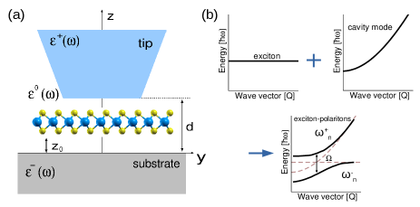
In such semiconducting microcavity setup the coupling between the exciton and cavity photon is expected to result in the splitting of exciton-polariton to the lower and upper polariton branches (LPB and UPB), which we shall refer as and , respectively [see Fig. 1(b)].
The quantity from which we extract the information about the electromagnatic modes in microcavity setup is electrical field propagator which, by definition Tomas , propagates the electrical field produced by point oscillating dipole , i.e. . Assuming that the 2D crystal, substrate and tip satisfy planar symmetry (in plane) the propagator in plane satisfies matrix equation
as illustrated by Feynmans diagrams in Fig. 2(a) (see also Sec. S1.A in Ref. sm ). Here represents the propagator of electrical field, in absence of 2D crystal, ie. when . The propagator represents the “free” electrical field and the propagator of scattered electrical field results in multiple reflections at the microcavity interfaces, as ilustrated in Fig. 2(b). In order to simplify the interpretation of the results we suppose that the dielectric media is vacuum (), and we suppose that tip and substrate are made of the same material (). In order to support well-defined cavity modes, these materials should be highly reflective in the exciton frequency region , which is satisfied if , where is the bulk plasmon frequency. For the P4 and WS2 monolayers where exciton energies are eV, we chose that the substrate and tip are made of silver ( eV). One the other hand, for the single-layer hBN where exciton energy is eV we chose aluminium ( eV). Both silver and aluminium macroscopic dielectric functions are determined as well from the first principles (see Ref. sm ). As an example, the intensity of electromagnatic modes () in silver microcavity is shown in Fig. S2 in Ref. sm . Figure 2(c) shows the perturbative expansion of optical conductivity ,
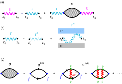
where is the RPA optical conductivity Pol ; Polariton2016 , while the ladder optical conductivity is , where is a normalization surface and are the current vertices. The -points polarizability satisfies the Dyson equation sm in which the Bethe-Salpeter-Fock kernel enters BSE1 ; BSE4 ; BSE9 ; GWtheory ; BSE8 . The electron energies are corrected using the GW method so that the present approach is equivlent to time-dependent screened Hartree-Fock approximation BSE1 ; BSE4 ; BSE8 ; GWtheory ; BSE9 ; BSE2 . For more details see Secs. S1.B and S2.B in Ref. sm . Without cavity photons, the total optical absorption Re in P4 and hBN is characterized with the strong excitons appearing at eV and eV, respectively. In addition, the absorption spectrum Re in WS2 shows the two spin-orbit splitted A and B excitons at eV and eV sm .
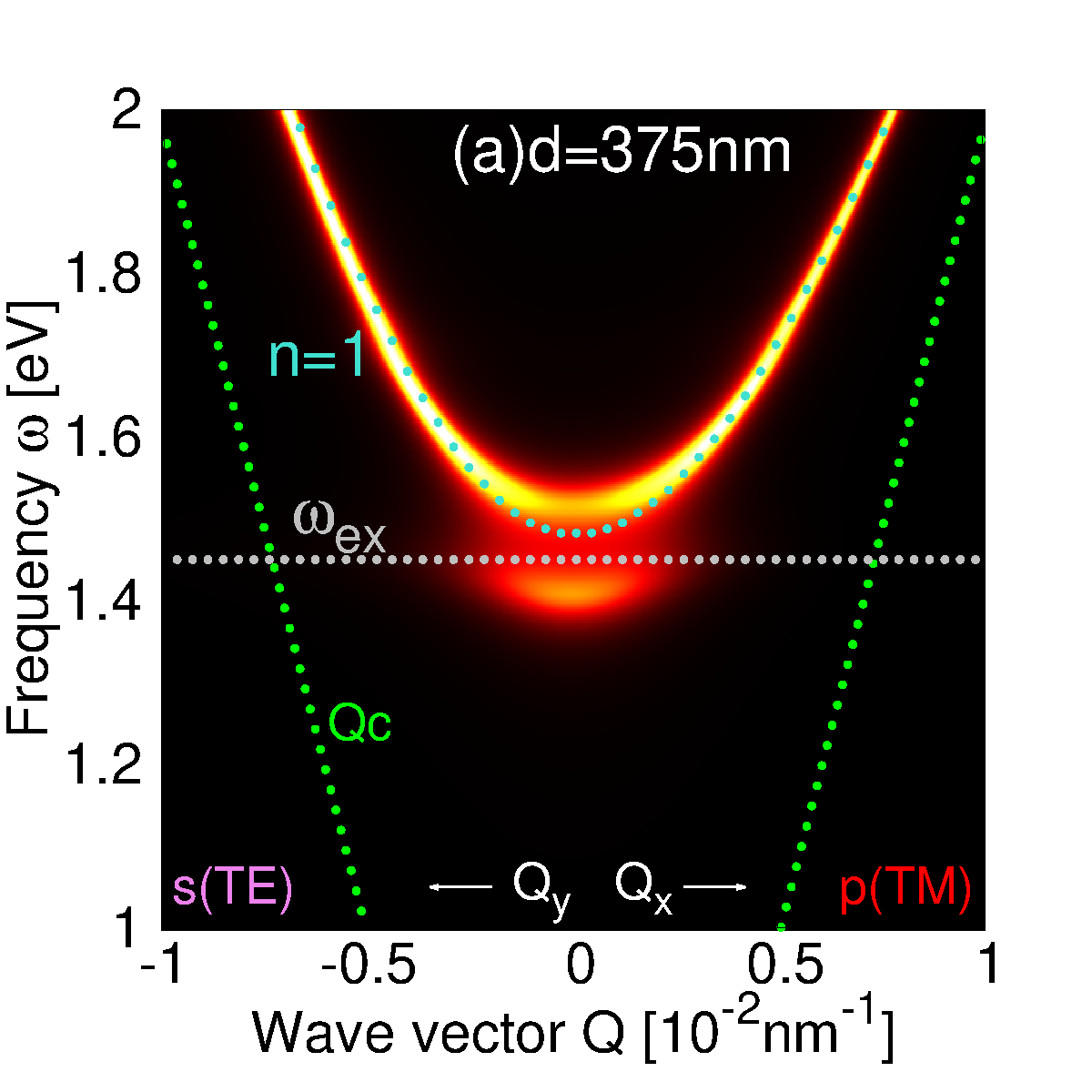
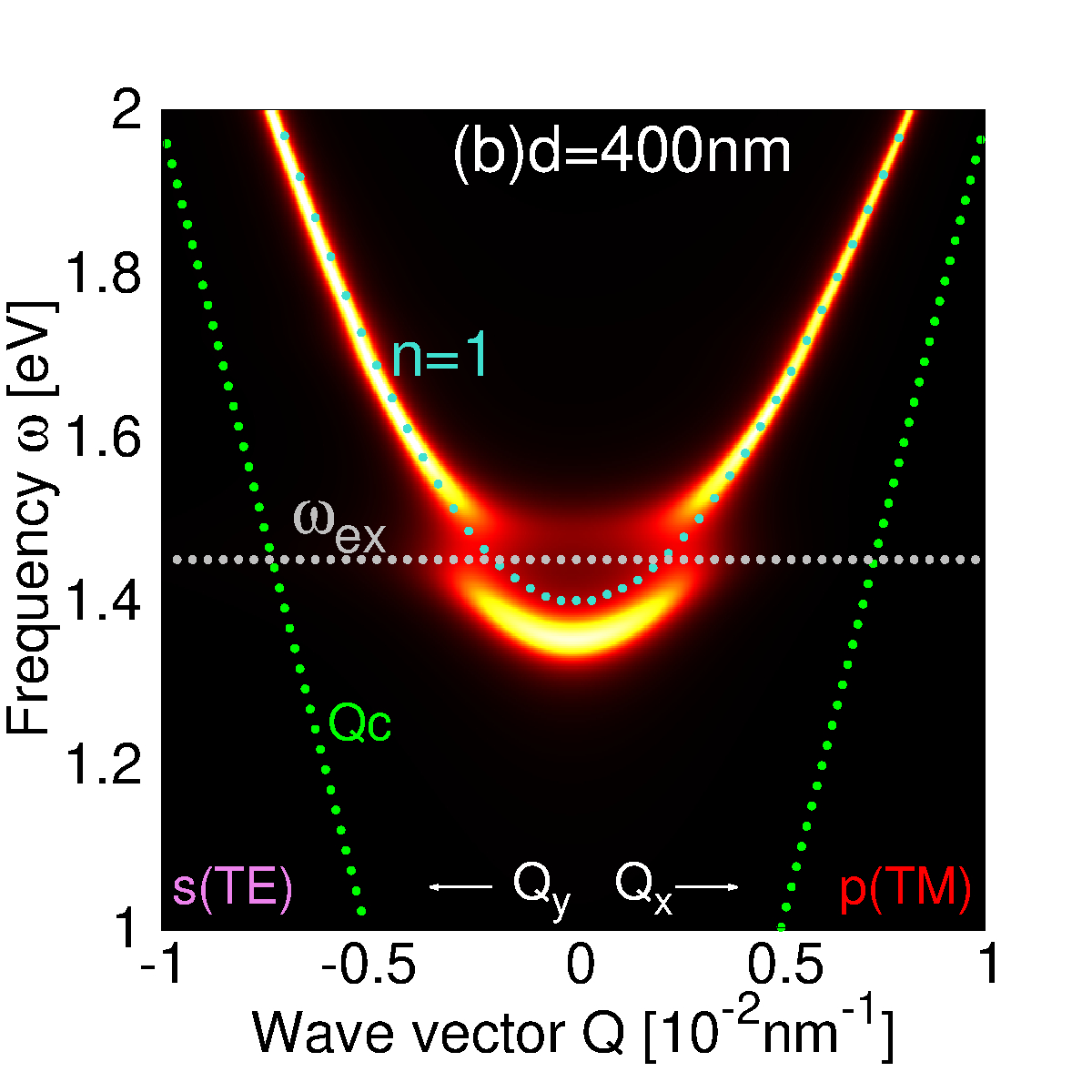
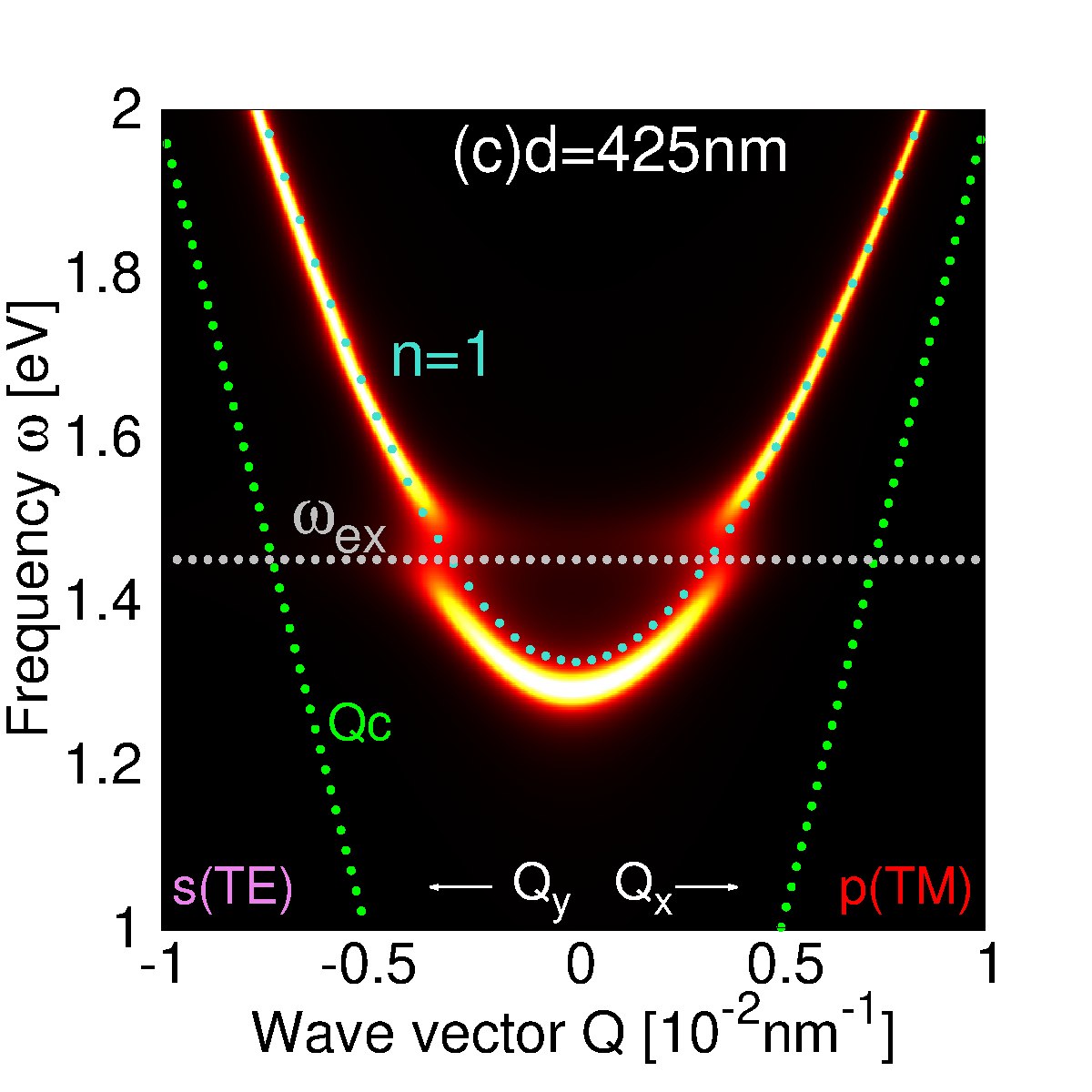
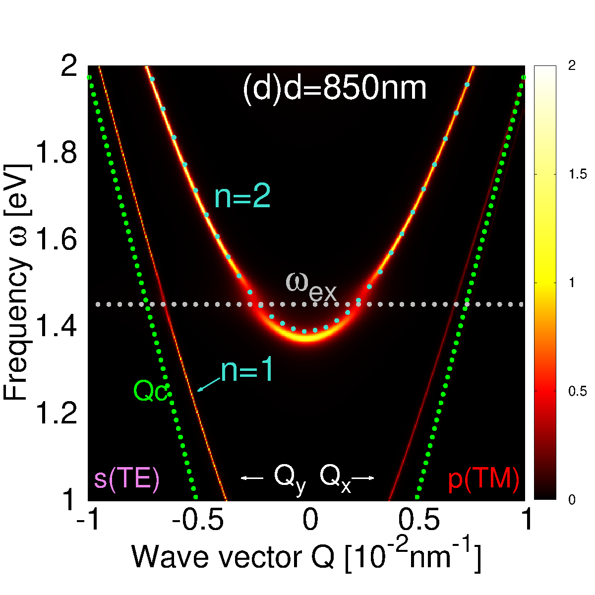
Figures 3(a), 3(b), and 3(c) show the modifications of the cavity mode intensity after the single-layer P4 is inserted in the middle =d/2 ( antinodal plane) of the silver cavity, where the cavity sizes are nm, nm and nm, respectively. White and turquoise dotted lines denote the P4 exciton and unperturbed cavity mode , respectively. For nm, just before the cavity mode crosses the exciton, a significant part of the mode spectral weight is transferred below the exciton energy. By increasing the cavity size, i.e. for nm and nm, the exciton crosses the mode, which results in the intensity weakening and band-gap oppening in the intersection area. This behaviour enables creation of exciton-polariton condensate, as experimentaly verified in Refs. bec3 ; ex-po-WSe2 ; Peroskite_ACSPhotonics ; ex-po-perovskite ; GaAsQW . By changing the cavity thickness, the exciton can interact also with the higher cavity modes. Figure 3(d) shows the modifications of mode intensity, where the cavity thickness is nm and P4 is choosen to be located at nm ( antinodal plane). The exciton significantly weakens the intensity of mode in the intersection area, however, here the avoided crossing behaviour is not clearly noticeable in comparison with the exciton coupled to the 1st cavity mode.
The dispersion relation of exciton-polaritons and (hybridised cavity photon-exciton modes), as the one shown in Fig. 4(a), can be precisely determined by following the splitted maxima in induced current driven by external (bare) field , where the screened optical conductivity is .
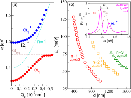
The inset of Figure 4(b) shows the Re before (brown dashed) and after (solid magenta) the P4 is inserted in the middle of the cavity of thickness nm. The spliting of exciton to exciton-polaritons and can be clearly seen. The exciton-photon binding strength can be determined from the Rabi splitting defined as difference for wave vector and for which the bare cavity modes crosses the exciton . Figure 4(a) shows the dispersion relations of plasmon-polaritons and obtained by following the splitted maxima in Re for different wave vectors , nm and . The clear anticrossing behaviour and Rabi splitting of meV indicates strong interaction between exciton and cavity photon. Red circles, yellow squares and green triangles in Fig. 4(b) show the Rabi splittings for , and , respectively, versus cavity thickness . The maximum Rabi splittings of th mode are achieved when and for choosen so that th mode just starts to cross the exciton energy . All three modes show strong coupling with exciton that results in the maximum splitings of meV, meV and meV for nm, nm and nm, respectively. For larger the cavity modes cross exciton at a greater angle and the splitting decreases. A decrease of as increases confirms a confinement hypothesis; as increases the cavity photon modes crosses the exciton for larger , and photon becomes less confined while the coupling is reduced. Thus, the coupling will be stronger as the thickness at which the crossing between th mode and exciton occurs is getting smaller.
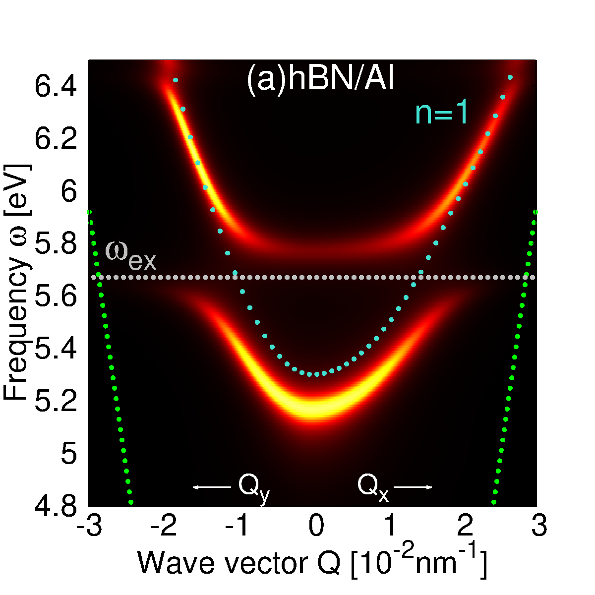
The above criterion is met by excitons with higher excitation energy, such as for instance the UV exciton in the hBN single layer. Since in the same UV frequency region the cavity should be highly reflective (i.e., ), the appropraite cavity for hBN layer can be made of aluminium with eV. Figure 5(a) shows the modification of aluminium cavity mode intensity after the hBN monolayer is inserted in the middle of cavity of thicknesses nm. The dotted lines show the unperturbed cavity mode and the hBN exciton. The strong exciton-photon intercation results in strong modification of the cavity mode, band-gap opening and Rabi splitting of meV. The maximum Rabi splitting of meV is achieved for nm. This large excion-polariton band gap and Rabi splitting suggest a possibility of experimental realization of robust exciton-polariton condensate in the cavity setup.
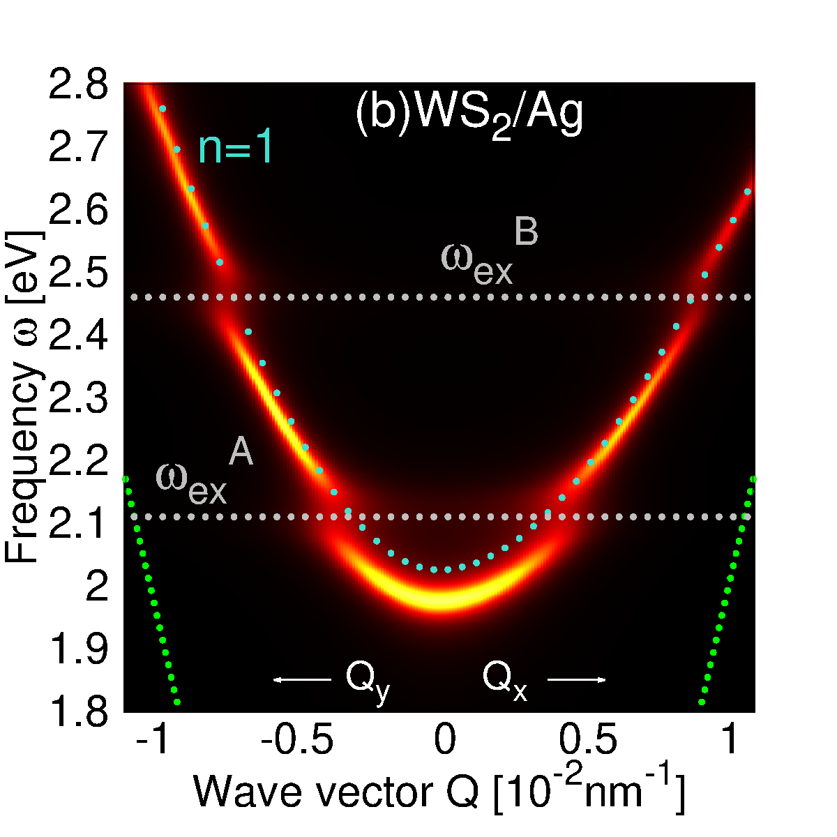
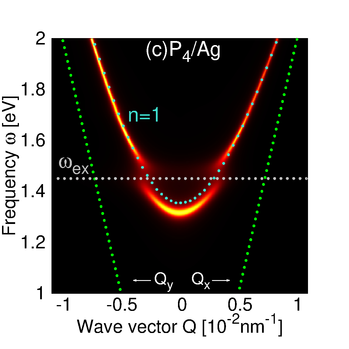
The 2D exciton-polaritons are experimentally studied mostly in various TMDs where the mesured Rabi splittings of meV, meV, and meV are found in MoS2 ex-pol1 , WSe2 ex-pol2 , and MoSe2 ex-pol22 . For WS2 the experimentally measured splittings are around meV for , depending on the precise cavity size ex-pol-WS2 . In Fig. 5(b) we show the modification of the silver cavity mode intensity when the WS2 monolayer is inserted in the middle of microcavity of thicknesse nm. The unperturbed mode as well as the A and B excitons of bare WS2 are also denoted by dotted lines. Both excitons significantly perturbe the mode providing the Rabi splitings of meV and meV. For comparison, Fig. 5(c) shows the modification of mode intensity when P4 is inserted in silver microcavity for the same conditions as in WS2 microcavity presented in Fig. 5(b); minimum is meV below the exciton. The cavity thickness is nm and . Interestingly, the achieved Rabi splittig is here also meV, even though according to confinement hypotesis, the A exciton, which is confined in smaller cavity, is expected to split more. However, the A exciton in WS2 has smaller oscillatory strength than P4 exciton [cf. Figs. S4(a) and S5(b) in Ref. sm ] so that the binding is weaker and the two effects cancel.
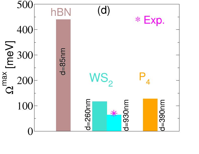
Finally, in Fig. 5(d) we compare the maximum splittings of exciton-polaritons for the three semiconducting microcavities, summarizing the different regimes of exciton-cavity photon coupling strengths in these materials. For WS2 microcavity we additionaly present the results for the experimentally measured value of cavity size, i.e., nm ex-pol-WS2 , when exciton interacts with cavity mode. The corresponding value of meV shows an excellent agreement with the experiment ex-pol-WS2 . For the same cavity thickness, splitting of the cavity mode and the WS2 A exciton is meV.
In summary, we have studied the intercation strengths between cavity photons and excitons in various 2D semiconducting crystals by means of rigorous ab initio methodology. It is shown that insertion of 2D crystals into a metallic microcavity significantly modifies the photon dispersion. For instance, the band gap opening and Rabi splitting as high as meV was obtained for hBN cavity device. This opens a possibility of experimental realization of the robust 2D exciton-polariton condensate. Moreover, the exciton-photon interaction strongly depends on photon confinement, which was shown to be adjustable by the cavity thickness . The results of exciton-polariton splitting in WS2 cavity device show a good agreement with recent experiments and suggest higher photon confinements with decreasing cavity size at which stronger photon-matter coupling should be achieved. In order reach this stronger binding we suggest an experimental setup consisting of tunable submicrometer cavity (such as AFM-tip and substrate) tuned so that the principal photon cavity mode coincide with the exciton energy, e.g. as in Fig.4(b).
Acknowledgements.
The authors acknowledge financial support from European Regional Development Fund for the “QuantiXLie Centre of Excellence” (Grant KK.01.1.1.01.0004) and “Center of Excellence for Advanced Materials and Sensing Devices” (Grant No. KK.01.1.1.01.0001), as well as from Croatian Science Foundation (Grant no. IP-2020-02-5556 and Grant No. UIP-2019-04-6869). Computational resources were provided by the Donostia International Physic Center (DIPC) computing center.References
- (1) D. N. Basov, Ana Asenjo-Garcia, P. James Schuck, Xiaoyang Zhu and Angel Rubio, Nanophotonics 10 549 (2021)
- (2) F. Schlawin, A. Cavalleri, and D. Jaksch, Phys. Rev. Lett. 122, 133602 (2019).
- (3) J. B. Curtis, Z. M. Raines, A. A. Allocca, M. Hafezi, and V. M. Galitski, Phys. Rev. Lett. 122, 167002 (2019).
- (4) J. Kasprzak, M. Richard, S. Kundermann et al., Nature 443, 409 (2006).
- (5) R. Balili, V. Hartwell, D. Snoke, L. Pfeiffer, and K. West, Science 316, 1007 (2007).
- (6) H. Deng, H. Haug, and Y. Yamamoto, Rev. Mod. Phys. 82, 1489 (2010).
- (7) A. Amo, J. Lefrère, Simon Pigeon et al., Nature Phys. 5, 805 (2009).
- (8) K. G. Lagoudakis, M. Wouters, M. Richard et al., Nature Phys. 4, 706 (2008).
- (9) C. Weisbuch, M. Nishioka, A. Ishikawa, and Y. Arakawa, Phys. Rev. Lett. 69, 3314(1992).
- (10) R. F. Ribeiro, L. A. Martínez-Martínez, M. Du, J. Campos-Gonzalez-Angulo, and J. Yuen-Zhou, Chem. Sci. 9, 6325 (2018).
- (11) S. Christopoulos, G. Baldassarri Höger von Högersthal, A. J. D. Grundy et al., Phys. Rev. Lett. 98, 126405 (2007).
- (12) J. J. Baumberg, A. V. Kavokin, S. Christopoulos et al., Phys. Rev. Lett. 101, 136409 (2008).
- (13) S. Zhang, J. Chen, J. Shi et al., ACS Photonics 7 327 2020.
- (14) W. Bao, X. Liu, F. Xue et al., PNAS 116, 20274 (2019).
- (15) T. Horikiri, T. Byrnes, K. Kusudo, N. Ishida, Y. Matsuo, Y. Shikano, A. Löffler, S. Höfling, A. Forchel, and Y. Yamamoto, Phys. Rev B 95, 245122 (2017).
- (16) A. Ramasubramaniam, Phys.Rev. B 86, 115409 (2012)
- (17) Y. Li, A. Chernikov, X. Zhang, A. Rigosi, H. M. Hill, A. M. van der Zande, D. A. Chenet, En-Min Shih, J. Hone, and T. F. Heinz, Phys. Rev. B 90, 205422 (2014)
- (18) D. Y. Qiu, F. H. Jornada, S. G. Louie, Phys. Rev. Lett. 111, 216805 (2013)
- (19) Y. Lin, X. Ling, L. Yu, S. Huang, Allen L. Hsu, Yi-Hsien Lee, J. Kong, M. S. Dresselhaus, and T. Palacios, Nano Lett. 14, 5569 (2014)
- (20) J. Yan, K. W. Jacobsen, K. S. Thygesen, Phys. Rev. B 86, 045208 (2012)
- (21) F. Ferreira and R. M. Ribeiro, Phys. Rev B 96, 115431 (2017)
- (22) C. E. P. Villegas, A. S. Rodin, A. C. Carvalho, and A. R. Rocha, Physical Chemistry Chemical Physics 18 (40) (2016)
- (23) X. Wang, A. M. Jones, K. L. Seyler, V. Tran, Yichen Jia, Huan Zhao, Han Wang, Li Yang, Xiaodong Xu and Fengnian Xia, Nature Nanotechnology 10, 517 (2015)
- (24) T. Low, A. Chaves, J. D. Caldwell, A. Kumar, N. X. Fang, P. Avouris, T. F. Heinz, F. Guinea, L. Martin-Moreno and Frank Koppens, Nature Materials 16, 182 (2017)
- (25) Xiaoze Liu, Tal Galfsky, Zheng Sun, Fengnian Xia, Erh-chen Lin, Yi-Hsien Lee, Stéphane Kéna-Cohen and Vinod M. Menon, Nature Photonics 9 (1) (2014)
- (26) S. Dufferwiel, S. Schwarz, F. Withers, A.A.P. Trichet, F. Li, M. Sich, O. Del Pozo-Zamudio, C. Clark 4, A. Nalitov, D.D. Solnyshkov, G. Malpuech, K.S. Novoselov, J.M. Smith, M.S. Skolnick, D.N. Krizhanovskii and A.I. Tartakovskii, Nature Communications 6, 8579 (2015)
- (27) L. C. Flatten, Z. He, D. M. Coles, A. A. P. Trichet, A. W. Powell, R. A. Taylor, J. H. Warner and J. M. Smith, Sci. Rep. 6, 33134 (2016).
- (28) S. Dufferwiel, T.P. Lyons, D.D. Solnyshkov, A.A.P. Trichet, A. Catanzaro, F. Withers, G. Malpuech, J.M. Smith, K.S. Novoselov, M.S. Skolnick, D.N. Krizhanovskii and A.I. Tartakovskii, Nature Communications 9, 4797 (2018)
- (29) Jie Gu, V. Walther, L. Waldecker, D. Rhodes, A. Raja, J. C. Hone, T. F. Heinz, Stéphane Kéna-Cohen, Thomas Pohl, Vinod M. Menon, arXiv:1912.12544
- (30) M. Förg, L. Colombier, R. K. Patel, J. Lindlau, A. D. Mohite, H. Yamaguchi, M. M. Glazov, D. Hunger and A. Högele, Nature Communications 10, 3697 (2019)
- (31) Z. Fei, M. E. Scott, D. J. Gosztola, J. J. Foley IV, J. Yan, D. G. Mandrus, H. Wen, P. Zhou, D. W. Zhang, Y. Sun, J. R. Guest, S. K. Gray, W. Bao, G. P. Wiederrecht, and X. Xu, Phys. Rev. B 94, 081402(R) (2016).
- (32) Z. Sun, J. Gu, A. Ghazaryan et al., Nature Photon. 11, 491 (2017).
- (33) M. Sidler, P. Back, O. Cotlet et al., Nature Phys. 13, 255 (2017).
- (34) D. S. Citrin and J. B. Khurgin, Phys. Rev. B 68, 205325 (2003).
- (35) J. Levinsen, Guangyao Li, and Meera M. Parish, Phys. Rev. Research 1, 033120 (2019)
- (36) Fei Xue, Fengcheng Wu, Ming Xie, Jung-Jung Su, and A. H. MacDonald, Phys. Rev. B 94, 235302 (2016)
- (37) Y. N. Gartstein, Xiao Li, and C. Zhang, Phys. Rev. B 92, 075445 (2015)
- (38) J. B. Khurgin, Optica 2, 740 (2015)
- (39) A. Krasnok, S. Lepeshov, and A. Alú, Optic Express 26, 12 (2018)
- (40) S. Latini, E. Ronca, U. De Giovannini, Hannes Hübener and A. Rubio, Nano Lett. 19, 3473 (2019).
- (41) D. Novko, K. Lyon, D. J. Mowbray, V. Despoja, (2021) in preparation.
- (42) See Supplemental Material at [URL] for more details on …
- (43) M. S. Tomaš, Phys. Rev. A 51, 2545 (1995)
- (44) V. Despoja, M. Šunjić, L. Marušić, Phys. Rev. B 80, 075410 (2009)
- (45) D. Novko, M. Šunjić, V. Despoja, Phys. Rev B 93, 125413 (2016)
- (46) L. Hedin, Phys. Rev. 139, A796 (1965)
- (47) G. Strinati, Phys. Rev. B 29, 5718 (1984)
- (48) G. Onida, L. Reining, A. Rubio, Rev. Mod. Phys. 74, 601 (2002)
- (49) Mark S. Hybertsen, Steven G. Louie, Phys. Rev. B 34, 5390 (1986)
- (50) M. Rohlfing, S. G. Louie, Phys. Rev. Lett. 81, 2312 (1998)
- (51) W. Hanke and L. J. Sham, Phys. Rev. Lett. 43, 387 (1979)