Lawrence Berkeley National Laboratory, Berkeley, CA 94720, USAbbinstitutetext: Walter Burke Institute for Theoretical Physics,
California Institute of Technology, Pasadena, CA 91125, USA
Extended Calculation of Dark Matter-Electron Scattering in Crystal Targets
Abstract
We extend the calculation of dark matter direct detection rates via electronic transitions in general dielectric crystal targets, combining state-of-the-art density functional theory calculations of electronic band structures and wave functions near the band gap, with semi-analytic approximations to include additional states farther away from the band gap. We show, in particular, the importance of all-electron reconstruction for recovering large momentum components of electronic wave functions, which, together with the inclusion of additional states, has a significant impact on direct detection rates, especially for heavy mediator models and at and higher energy depositions. Applying our framework to silicon and germanium (that have been established already as sensitive dark matter detectors), we find that our extended calculations can appreciably change the detection prospects. Our calculational framework is implemented in an open-source program EXCEED-DM (EXtended Calculation of Electronic Excitations for Direct detection of Dark Matter), to be released in an upcoming publication.
1 Introduction
Electronic excitations have been established as an alternative to nuclear recoils in direct detection of sub-GeV dark matter (DM). Nuclear recoil searches lose sensitivity at lower DM masses due to kinematic mismatch between the DM and heavier nuclei, whereas electronic transitions can potentially extract all of the DM kinetic energy during a DM-electron scattering event by excitation across an energy gap. Proposed targets, including noble gas atoms with ionization energies Essig:2011nj ; Graham:2012su ; Lee:2015qva ; Essig:2017kqs ; Catena:2019gfa ; Agnes:2018oej ; Aprile:2019xxb ; Aprile:2020tmw , semiconductors with electronic band gaps Essig:2011nj ; Graham:2012su ; Essig:2012yx ; Lee:2015qva ; Essig:2015cda ; Derenzo:2016fse ; Hochberg:2016sqx ; Bloch:2016sjj ; Kurinsky:2019pgb ; Trickle:2019nya ; Griffin:2019mvc ; Griffin:2020lgd ; Du:2020ldo , and superconductors and Dirac materials with band gaps Hochberg:2015pha ; Hochberg:2015fth ; Hochberg:2016ajh ; Hochberg:2017wce ; Coskuner:2019odd ; Geilhufe:2019ndy ; inzani2021prediction , extend the reach on DM mass well below the limit of nuclear recoil. Experimental searches using dielectric crystal targets are currently underway, specifically with Si (DAMIC deMelloNeto:2015mca ; Aguilar-Arevalo:2019wdi ; Settimo:2020cbq , SENSEI Tiffenberg:2017aac ; Crisler:2018gci ; Abramoff:2019dfb ; Barak:2020fql , SuperCDMS Agnese:2014aze ; Agnese:2015nto ; Agnese:2016cpb ; Agnese:2017jvy ; Agnese:2018col ; Agnese:2018gze ; Amaral:2020ryn ) and Ge (EDELWEISS Armengaud:2018cuy ; Armengaud:2019kfj ; Arnaud:2020svb , as well as SuperCDMS) which have been predicted to have excellent sensitivity down to DM masses based on their band gaps.
Reliable theoretical predictions of target-specific transition rates are important not only for current experiments, but also for planning the next generation of detectors. Compared to the DM-induced electron ionization rate in noble gases like xenon Essig:2011nj ; Graham:2012su ; Lee:2015qva ; Essig:2017kqs ; Catena:2019gfa ; Agnes:2018oej ; Aprile:2019xxb ; Aprile:2020tmw , calculations for the DM-electron scattering rate in a crystal are more complicated. Ionization rates for noble gases can be calculated by considering each noble gas atom as an individual target, where the calculation simplifies to finding the ionization rate from an isolated atom, for which the wave functions and energy levels are well tabulated Bunge:1993jsz . However, for crystal targets the atoms are not isolated and more involved techniques are required to obtain an accurate characterization of DM-electron interactions in a many-body system.
There have been a variety of approaches taken to compute the DM-electron scattering rate in crystals. One of the first attempts, Ref. Graham:2012su , computed the rate with semi-analytic approximations for the initial and final state wave functions, and used the density of states to incorporate the electronic band structure. Later, Ref. Lee:2015qva continued in this direction and used improved semi-analytic approximations for the initial state wave functions. Meanwhile, a fully numerical approach was advanced in Refs. Essig:2011nj ; Essig:2015cda ; Derenzo:2016fse where density functional theory (DFT) was employed to calculate the valence and conduction electronic band structures and wave functions. The latter approach, as implemented in the QEdark program and embedded in the Quantum ESPRESSO package QE-2009 ; QE-2017 ; doi:10.1063/5.0005082 , has become the standard for first-principles calculations of DM detection rates. Recently, in Refs. Trickle:2019nya ; Griffin:2019mvc we used a similar DFT approach as implemented in our own program for a study of DM-electron scattering in a variety of target materials. More recently there has been work utilizing the relation between the dielectric function and the spin-independent scattering rate Hochberg:2021pkt ; Knapen:2021run ; Knapen:2021bwg , which also properly incorporates screening effects.
The goal of this work is to further extend the DM-electron scattering calculation in several key aspects, and present state-of-the-art predictions for Si and Ge detectors using a combination of DFT and semi-analytic methods. As we will elaborate on shortly, the time- and resource-consuming nature of DFT calculations presents an intrinsic difficulty that has limited the scope of previous work in this direction to a restricted region of phase space; typically only bands within a few tens of eV above and below the band gap were included and electronic wave functions were cut off at a finite momentum. We overcome this difficulty by implementing all-electron (AE) reconstruction (whose importance was previously emphasized in Ref. Liang:2018bdb ) to recover higher momentum components of DFT-computed wave functions, and by extending the calculation to bands farther away from the band gap using semi-analytic approximations along the lines of Refs. Graham:2012su ; Lee:2015qva . As we will see, the new contributions computed here have a significant impact on detection prospects in cases where higher energy and/or momentum regions of phase space dominate the rate, including scattering via a heavy mediator, and experiments with or higher energy thresholds. We also stress that in contrast to the recent work emphasizing the relation between spin-independent DM-electron scattering rates and the dielectric function Hochberg:2021pkt ; Knapen:2021run ; Knapen:2021bwg , our calculation can be straightforwardly extended to DM models beyond the standard spin-independent coupling. Furthermore, we do not make assumptions about isotropy for the majority of our calculation, and our framework is capable of treating anisotropic targets which exhibit smoking-gun daily modulation signatures Coskuner:2019odd ; Trickle:2019nya ; Geilhufe:2019ndy (see also Refs. Griffin:2018bjn ; Coskuner:2021qxo for discussions of daily modulation for phonon excitations).
Our calculation is implemented in an open-source program EXCEED-DM (EXtended Calculation of Electronic Excitations for Direct detection of Dark Matter), to be released in an upcoming publication. Currently a beta version of the program is available here tanner_trickle_2021_4747696 . We also make available our DFT-computed wave functions Trickle2021 and the output of EXCEED-DM Trickle2021a for Si and Ge.
1.1 Overview of the Calculation and Key Results
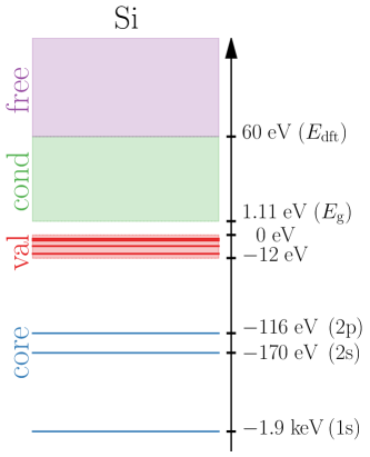
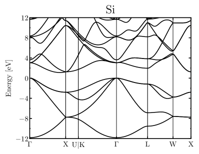
Before delving into the technical details, let us give a brief overview of the calculation and highlight some key results. We divide the electronic states in a (pure) crystal into four categories: core, valence, conduction and free, as illustrated in Fig. 1 for Si and Ge and discussed in more detail in Sec. 2. At zero temperature, electrons occupy states up to the Fermi energy, defined as the maximum of the valence bands and denoted by . The band gap , i.e. the energy gap between the occupied valence bands and unoccupied conduction bands, is typically for semiconductors, e.g. 1.11 eV for Si and 0.67 eV for Ge; this sets a lower limit on the energy deposition needed for an electron transition to happen.
The electronic states near the band gap deviate significantly from atomic orbitals and need to be computed numerically. We apply DFT methods (including AE reconstruction) for this calculation, and refer to the DFT-computed states as valence and conduction. Specifically, for both Si and Ge, we take the first four bands below the gap to be valence, which span an energy range of eV to 0 and eV to 0, respectively, and take bands above the gap up to eV to be conduction.
With more computing power we can in principle include more states, both below and above the band gap, in the DFT calculation. However, since the states far from the band gap can be modeled semi-analytically with reasonable accuracy, computing them with DFT is inefficient. Below the valence bands, electrons are tightly bound to the atomic nuclei. We model them using semi-analytic atomic wave functions and refer to them as core states. These include the 1s, 2s, 2p states in Si and 1s, 2s, 2p, 3s, 3p, 3d states in Ge (the 3d states in Ge are sometimes referred to as semi-core, and we will compare the DFT and semi-analytic treatment of them in Secs. 2.2 and 3.3). Finally, above eV, we model the states as free electrons as they are less perturbed by the crystal environment.
With the electronic states modeled this way, we compute the rate for valence to conduction (vc), valence to free (vf), core to conduction (cc) and core to free (cf) transitions induced by DM scattering, as discussed in detail in Sec. 3. The total rate is the sum of all four contributions. We then use our calculation to update the projected reach of direct detection experiments in Sec. 4, and compare our results with previous literature.
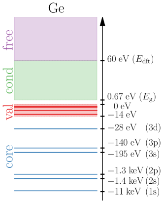
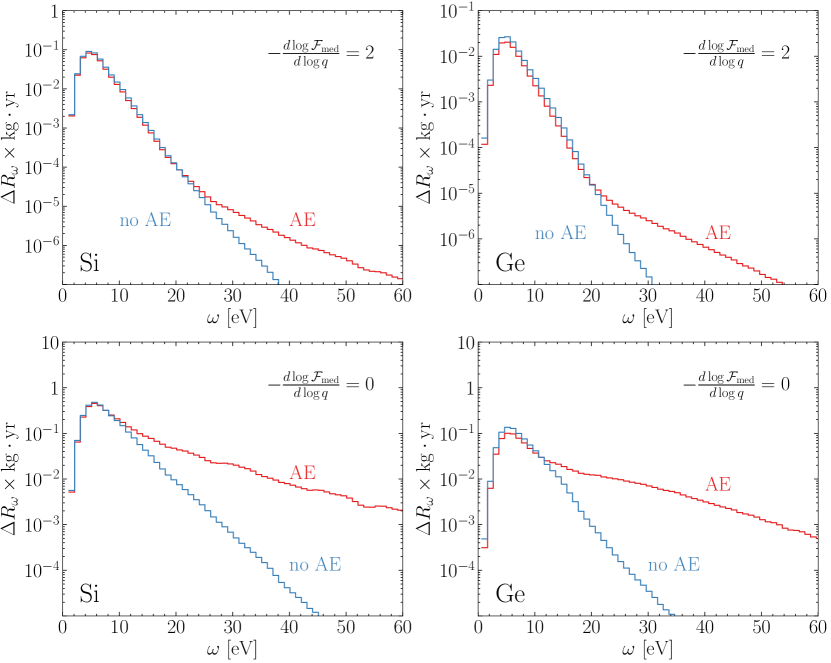
Figure 2 gives a glimpse of some of our key results. Here we consider the case of DM scattering via a heavy mediator in a Ge target. The impact of core (3d) to conduction contributions is clearly visible from both the differential rate (left panel, for GeV) and the projected reach (right panel). They dominate the total rate for MeV, and, as we can see from the right panel of Fig. 2, lead to significantly more optimistic reach compared to previous DFT calculations implemented in QEdark Essig:2015cda ; Derenzo:2016fse ; this is especially true for higher detector thresholds (corresponding to higher values). Note that while Refs. Essig:2015cda ; Derenzo:2016fse included the 3d states in their DFT calculation, their contributions were significantly underestimated due to the absence of AE reconstruction. The importance of AE reconstruction is also seen from the valence to conduction differential rate in the left panel of Fig. 2, where our calculation predicts a much higher rate at eV compared to the QEdark calculation in Ref. Derenzo:2016fse . Meanwhile, accounting for in-medium screening (see Sec. 3.5) we find, consistent with Ref. Knapen:2021run , a lower rate at energy depositions just above the band gap, and as a result, weaker reach at low , compared to Refs. Essig:2015cda ; Derenzo:2016fse . On the other hand, our modeling of the core (3d) states is similar to the semi-analytic approach of Ref. Lee:2015qva , and indeed we find very similar reach at large ; however, the approach of Ref. Lee:2015qva overestimates the rate at smaller due to reduced accuracy in the modeling of the valence and conduction states. We reserve a more detailed comparison with the literature for Sec. 4.1.
2 Electronic States
To compute the DM-electron scattering rate one must understand the electronic states of the target. In targets with a periodic potential, Bloch’s theorem states that the energy eigenstates can be indexed by a momentum, , which lies within the first Brillouin zone (1BZ). These Bloch states, , where represents additional quantum numbers, are eigenstates of the discrete translation operator such that , which means the electronic wave functions can be written as
| (1) |
where and is the target volume. For every there exists a tower of eigenstates (labeled by ) of the target Hamiltonian which constitutes the complete set of states in the target. Unfortunately this complete set is not known for a general material and therefore a combination of approximations must be used to calculate them. As discussed in Sec. 1.1 and illustrated in Fig. 1, we divide the states into core, valence, conduction and free, and use a combination of numerical calculations and semi-analytic modeling. In this section, we expand on the treatment of each type of electronic states.
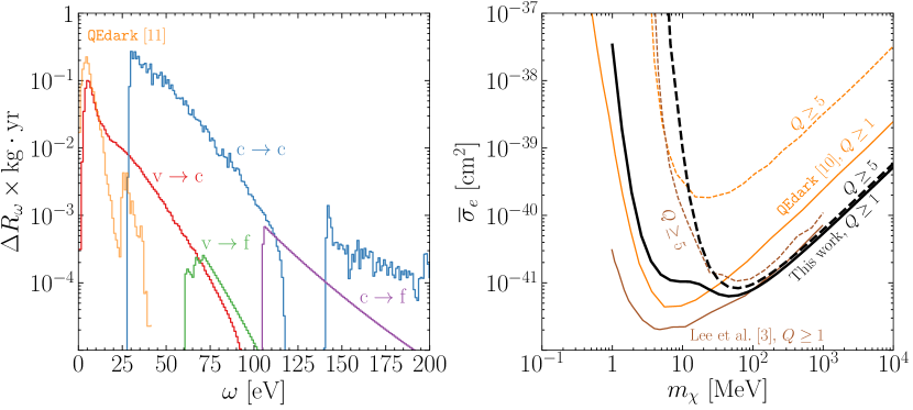
We first discuss the DFT calculation for valence and conduction states in Sec. 2.1, and then move on to explain the semi-analytic treatment of core states in Sec. 2.2. Our main results are contained in Fig. 3 where we compare the average magnitude of electronic wave functions, binned in momentum (see Eq. (7)), computed with and without AE reconstruction, discussed further in Sec. 2.1.1, and, for the highest energy core states (2p in Si and 3d in Ge), those computed using the core approximation discussed in Sec. 2.2. We find that the AE reconstruction includes a significant contribution from wave functions at large momentum as expected, and that for the core states, the semi-analytic approach reproduces the large momentum components of these AE reconstructed DFT wave functions. Lastly we will discuss the analytic treatment of the free states in Sec. 2.3.
2.1 DFT Wave Functions and Band Structures
In principle, DFT provides an exact solution to the many-electron Schrödinger equation by the Hohenberg-Kohn theorems that treat all properties of a quantum many-body system as unique functionals of the ground state density. They further show that the exact ground state density and energy can be found by minimizing the total energy of the system Hohenberg:1964zz ; martin2020electronic . This becomes tractable by the Kohn-Sham (KS) equations that reduce the many-body problem to non-interacting electrons moving in an effective potential, ,
| (2) |
where is the orbital energy of the KS orbital Kohn:1965zzb . The external potential and Hartree potential , are known, while the exchange-correlation (xc) potential , which contains the many-body interactions, must be approximated. Herein lies the deviation from the exact solution, and although various formulations of xc-energy functionals have been successful, the choice of xc-functional will affect the predicted electronic states and hence calculated transition rates. For Si, we use PBE Perdew1996 , a type of generalized gradient approximation (GGA) xc-functional which is one of the most popular and low-cost choices. Local and semi-local based xc-functionals, such as PBE, suffer from a self-interaction error and band gap underestimation, which we modify with a “scissor correction” where the bands are shifted to match the experimentally determined values of band gap. For Ge, this underestimation results in zero band gap with PBE, therefore we instead use a hybrid functional, which mixes a parameterized amount of exact exchange into the xc-functional, correcting band gaps and band widths by error cancellation at the cost of increased computation time. We use the range-separated hybrid functional HSE06 Heyd2003a ; Heyd2006 , which applies a screened Coulomb potential to correct the long-range behavior of the xc-potential, giving high accuracy at a mid-level computational cost. Our computed band structures for Si and Ge are shown in Fig. 4.
The periodic Bloch wave functions, , Eq. (1), for band and Bloch wave vector are computed by finding the Fourier coefficients, (which satisfy the normalization condition, ):
| (3) |
The number of reciprocal lattice vectors kept in the sum is conventionally set by an energy cutoff, , such that . These Bloch wave function coefficients for both Si and Ge are computed with the projector augmented wave (PAW) method Blo ; Kresse1999 within vasp Kresse1993 ; Kresse1994 ; Kresse1996 ; Kresse1996a up to keV on a uniform mesh over the 1BZ. We then include AE reconstruction effects up to a higher energy cutoff, keV, which recovers higher momentum components of the wave functions up to , as discussed in more detail in Sec. 2.1.1. The Bloch wave function coefficients, , for Si and Ge used for this work can be found here Trickle2021 .
A final consideration of using DFT wave functions is that DFT is fundamentally a ground state method, and the KS conduction band states are only approximations to excited states. Excited state methodologies are much more computationally expensive than ground state KS-DFT. Furthermore, since excited state quasiparticles, such as excitons, have been argued to have a negligible effect on the calculation of DM scattering rates Derenzo:2016fse , they are neglected in our calculations.
2.1.1 All-electron Reconstruction
There are many different approaches to find the eigenstates of Eq. (2). The PAW method Blo is one such standard approach. The main idea of the PAW method is to split up the calculation of the eigenstates: near the ionic centers the wave functions resemble the eigenstates of an isolated atom, while further away they can be computed numerically with a pseudopotential. This greatly simplifies the numeric calculation since the focus is then on large distance (small momentum), and the small distance (high momentum) pieces can be self-consistently reintroduced after the main part of the DFT calculation. The large distance components of the wave function are known as “pseudo wave functions” (PS wave functions) and the total wave functions are known as the “all-electron wave functions” (AE wave functions), indicating that all of the wave function components are included. We will now give a brief overview of how the AE wave functions can be reconstructed from the PS wave functions, computed with PAW-based DFT codes, and refer the reader to Refs. Blo ; Kresse1999 ; rostgaard2009projector ; pawpy for more detailed information.111It is possible to calculate all electronic eigenstates, including the core, self-consistently by other more complex methods such as the full-potential linearized augmented plane wave (FP-LAPW) method or the relaxed-core PAW (RC-PAW) method.
The AE wave functions, are built from two components. Near the ionic core, or inside an “augmentation sphere,” is expanded in a set of basis functions, , which are simply taken to be the wave functions of an isolated atom,
| (4) |
Outside of the augmentation sphere, . Near the ionic core the PS wave functions are expanded in a set of basis functions that are computationally more convenient than the . Therefore,
| (5) |
which simply replaces the components in within the augmentation sphere with the AE wave function. To find the coefficients we insert an identity, , where are projector functions, defined to satisfy this identity within the augmentation sphere. Therefore, , . The last ingredient to compute from is to require that is related to via a transformation, . This implies that all the PS states are related to AE states by this transformation , such that and the AE reconstruction can be written as
| (6) |
In practice, we implement the AE reconstruction with pawpyseed pawpy , and the plane wave expansion cutoff of , , can be increased from the initial . We use keV.
To visualize the effect of AE reconstruction, we plot in Fig. 3 the average magnitude of the Bloch wave functions, binned in ,
| (7) |
where are the Fourier components of the Bloch wave functions, defined in Eq. (3). Each bin in momentum space extends from to with keV, and is a normalization factor equal to the number of points in a bin, . We see that AE reconstruction recovers the high momentum components, which as we will see can significantly affect the DM-induced transition rate for processes which favor large momentum transfers (such as processes mediated by heavy particles), or processes limited to larger (e.g. higher experimental thresholds where large processes are the only kinematically allowed transitions). Previous DFT calculations of DM-induced electron transition rates, with the exceptions of Ref. Liang:2018bdb ; Trickle:2019nya ; Griffin:2019mvc , used only the pseudo wave functions, as opposed to the AE wave functions, , and have therefore underestimated detection rates in several cases.
2.2 Atomic Wave Functions
If one could reconstruct the AE wave functions arbitrarily deep into the band structure, and to arbitrarily high momentum, one could calculate an accurate representation of the complete set of electronic states with a DFT calculation. In practice, however, this is neither feasible nor necessary. States deep in the band structure are more isolated from the influence of the crystal environment, and so an isolated atomic approximation becomes valid. We refer to these inner, tightly bound electrons as core electrons. In Si, we will show that the 2p states and below can be treated as core, while in Ge, the 3d states and below can, as alluded to in Fig. 1. The purpose of this subsection is to expand on the atomic approximation for core electrons and discuss its accuracy.
More precisely, the initial states of a transition should be taken as a linear combination of isolated atomic wave functions that is in Bloch form (known as Wannier states):
| (8) |
where labels the atom in the primitive cell, are the standard atomic quantum numbers, is the equilibrium position of the atom, sums over all primitive cells in the lattice, and is the total number of cells. In contrast to the valence and conduction states discussed in the previous subsection, the core states are labeled by rather than band index . The corresponding periodic (dimensionless) functions can be easily obtained via Eq. (1):
| (9) |
where is the primitive cell volume.
In general, the atomic wave functions are not known analytically, but are expanded in a basis of well-motivated analytic functions. The basis coefficients are then fit by solving the isolated atomic Hamiltonian, giving a semi-analytic expression for . We use a basis of Slater type orbital (STO) wave functions whose radial component is
| (10) |
where Å is the Bohr radius, and is an effective charge of the ionic potential. Including the angular part, the atomic wave functions are then
| (11) |
where are tabulated in Ref. Bunge:1993jsz , and are the spherical harmonics with the Condon-Shortley phase convention E.U.Condon1935 .
To assess the accuracy of the atomic wave function approximation, we temporarily push the DFT calculation beyond its default regime (valence and conduction), to the highest core states – 2p states in Si and 3d states in Ge, where it is still computationally feasible – and compare the numerical wave functions to the semi-analytic ones discussed above. The results, in terms of the average magnitude of Bloch wave functions defined in Eq. (7), are shown in the right panels of Fig. 3.222The flatness of band structures offers a complementary check of the validity of the atomic approximation. We have verified that the DFT computed energy eigenvalues indeed have a small variance for the highest core states, as expected. We see that the atomic approximation accurately reproduces the numerical wave functions up to the momentum cutoff keV for keV. These plots also show the limitation of DFT calculations. While AE reconstruction recovers higher-momentum components of electronic wave functions, it is not feasible to expand the plane wave basis set to arbitrarily high cutoff. However, having verified the atomic approximation for the highest core states, we can use it for all core states with confidence, allowing us to more easily include the high momentum components beyond the DFT cutoff.
2.3 Plane Wave Approximation
With the inclusion of the semi-analytic core states, all of the states below the band gap have been modeled. States above the band gap can also be computed with DFT methods, as described in Sec. 2.1. Similar to valence bands, there are practical limitations to how many conduction bands can be included. To remedy this in the simplest way possible, we model states far above the band gap as plane waves,
| (12) |
where is a reciprocal lattice vector, and plays the role of a band index. (To understand this, simply note that every momentum can be decomposed into a vector inside the 1BZ and a reciprocal lattice vector. Integrating over the momentum of plane wave states amounts to a integral within the 1BZ and a sum.) From Eq. (1) we see that the corresponding periodic functions are simply
| (13) |
The plane wave approximation is often used in atomic ionization rate calculations, with the inclusion of a Fermi factor, ,
| (14) |
where is the final state electron energy, and is an effective charge parameter, which enhances the transition rate at low to account for the long range behavior of the Coulomb potential. See Refs. Essig:2011nj ; Graham:2012su ; Lee:2015qva ; Agnes:2018oej for more details. In atomic ionization calculations one usually takes to be related to the binding energy of the initial state, ,
| (15) |
where is the principal quantum number. Since the rate is proportional to the Fermi factor, is seen as the conservative choice. Later in Secs. 3.2 and 3.4 we quantify how much of an effect this has on the transition rate. This uncertainty is only important for very high experimental thresholds, and generally we find that leads to a smoother match (within an factor) to conduction band contributions from DFT calculations.
3 Electronic Transition Rates
We now present the DM-induced electron transition rate calculation. We begin with a general discussion and then in Secs. 3.1-3.4 consider the four different transition types in turn: valence to conduction (), valence to free (), core to conduction () and core to free (). Finally, in Sec. 3.5 we discuss the treatment of in-medium screening.
The general derivation has been discussed previously (see e.g. Refs. Graham:2012su ; Essig:2015cda ; Catena:2019gfa ; Trickle:2019nya ; Liang:2018bdb ), and we repeat it here for completeness and clarity, as a variety of conventions have been used. Beginning with Fermi’s Golden Rule, the transition rate between electronic states and due to scattering with an incoming non-relativistic DM particle, , with mass , velocity , and spin is given by
| (16) |
where , is the momentum deposited onto the target, , , is the interaction Hamiltonian, is total volume of the target, and is the energy deposition:
| (17) |
We assume that all quantum states are unit normalized. Modulo in-medium screening effects, discussed below in Sec. 3.5, we can write Eq. (16) in terms of the standard QFT matrix element, defined with plane wave incoming and outgoing states, by inserting and using
| (18) |
We find
(19)
where .
We will limit our analysis to matrix elements which only depend on , and assume that the electron energy levels are also spin independent, which allows the spin sums to be easily computed:
| (20) | ||||
| (21) |
where is the spin averaged matrix element squared and we have defined a crystal form factor , written in terms of both momentum and position space representations of the wave functions.
The transition rate per target mass, , is then given by
| (22) |
where is the target density, is the local DM density, and is taken to be a boosted Maxwell-Boltzmann distribution. The total rate, , is then simply the sum over all possible transitions from initial to final states. Since the only dependence in Eq. (22) comes from the energy conserving delta function, we perform the integral first and define . This integral can be evaluated analytically (see e.g. Refs. Coskuner:2019odd ; Trickle:2019nya ; Coskuner:2021qxo ):
| (23) | ||||
| (24) |
where is the deposited energy, and is a normalization factor such that . We take the DM velocity distribution parameters to be kms , kms, and kms. The total rate then becomes
| (25) |
Here we focus on simple DM models, such as the kinetically mixed dark photon or leptophilic scalar mediator models. In these models can be factorized as , where for a heavy mediator and for a light mediator, and is a screening factor discussed in more detail in Sec. 3.5. As in previous works, we choose the reference momentum transfer to be . We can then finally write the rate in terms of a reference cross section,
| (26) |
and find
| (27) |
Another useful quantity is the binned rate (the rate for energy deposition between and ), , defined as
| (28) |
3.1 Valence to Conduction
We begin with valence to conduction band transitions. The initial (final) states are indexed by band number, , and Bloch momentum, inside the 1BZ. The wave functions in Eq. (1) can be substituted into the crystal form factor in Eq. (21),
| (29) |
where the integral is over the primitive cell with volume , and we have used the identity . The total rate in Eq. (27) is then
| (30) |
where , is the number of valence (conduction) bands. This is identical to the rate formulae derived in Griffin:2019mvc ; Trickle:2019nya ; Essig:2015cda but written in terms of the periodic Bloch functions, , instead of their Fourier transformed components, , similar to Ref. Liang:2018bdb . Numerically the position space form is superior since the integral over the primitive cell can be computed by Fast Fourier Transform. This reduces the computational complexity from to , where is the number of points, i.e. the number of Fourier components in the expansion of in Eq. (3).
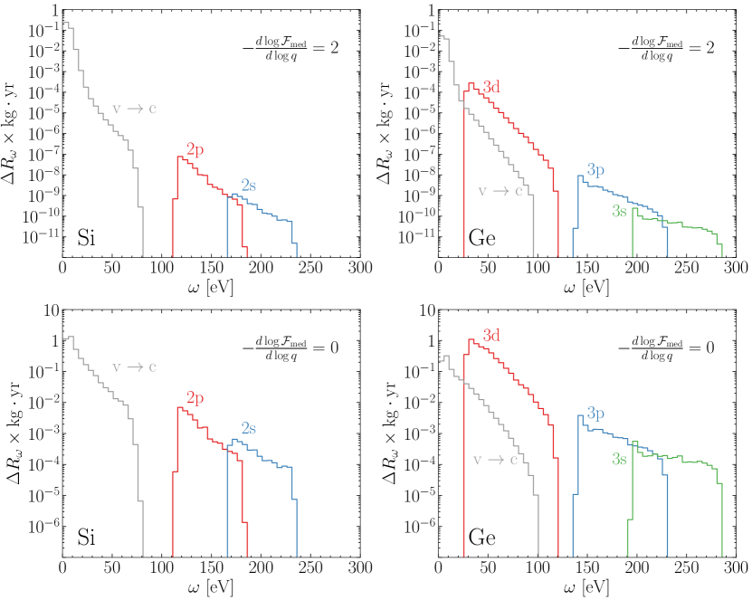
In Fig. 5 we show the scattering rate from valence to conduction transitions binned in energy deposition, defined in Eq. (28), for a 1 GeV DM. The main difference between the calculation performed here and in previous works is the effect of the AE reconstruction, as discussed in Sec. 2.1.1. For the case of DM with a heavy mediator, the rate, even with experimental thresholds as low as eV, is significantly enhanced relative to previous work. The AE reconstruction plays less of a role in the light mediator case since the transition rate is dominated by small momentum transfers. However, at high thresholds, where only larger momentum components can contribute, the AE reconstruction can still significantly boost the scattering rate by fully including the contributions neglected in the pseudo wave functions.
Since most earlier works computing DM-electron scattering include only valence to conduction transitions, it is useful to understand for which DM masses these are the only kinematically allowed transitions. If , where is the maximum energy of the core states, then the core states cannot contribute; if the free states are not available. Therefore if only the valence to conduction transitions are allowed, which can be related to a DM mass via , where
| (31) |
with , the maximum incoming DM velocity. For Si (Ge), eV ( eV), this corresponds to
| (32) |
Requiring that , where is the band gap, sets a lower bound on the minimum detectable mass, ,
| (33) |
For Si (Ge), with a band gap of 1.11 (0.67) eV, is () MeV. Lastly, we remark that for DM interactions characterized by higher-dimensional operators (not considered in this work), the scattering rate scales with higher powers of and therefore is even more sensitive to AE reconstruction (and also contributions discussed below in Sec. 3.3), which must be included in the analysis.
3.2 Valence to Free
For valence to free transitions the initial states are identical to those from Sec. 3.1, labeled by band number and Bloch momentum, . The final state wave functions are simple plane waves given by Eq. (12), labeled by a momentum in the 1BZ with the bands labeled by . We can therefore directly substitute Eq. (13) into Eq. (29) derived in the previous subsection, and obtain the crystal form factor:
| (34) |
where are the Fourier components of the Bloch wave functions defined in Eq. (3). Incorporating the Fermi factor correction discussed in Sec. 2.3, we find the rate in Eq. (27) is given by
| (35) |
where
| (36) |
With a change of variables, and defining (and then dropping the prime for simplicity), the rate becomes
| (37) |
where .
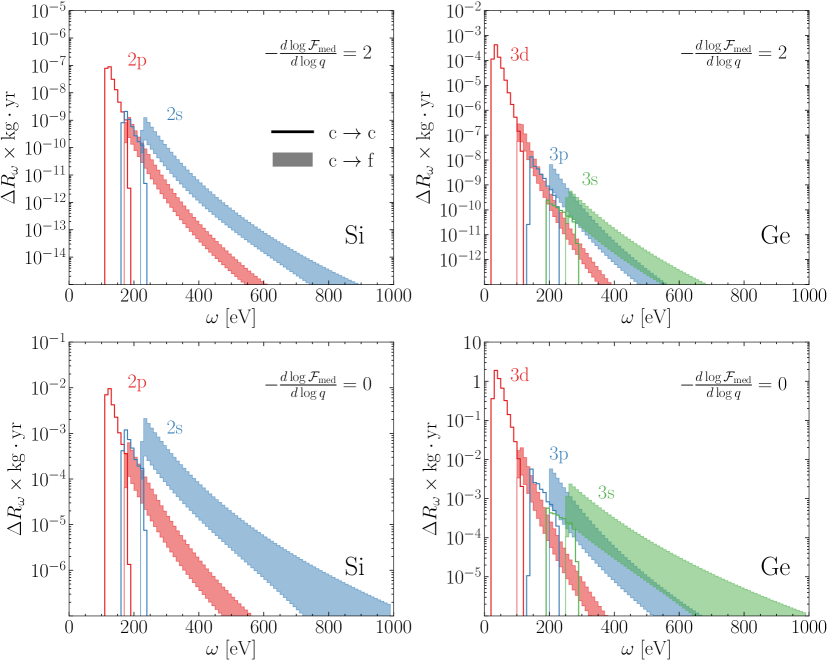
In Fig. 6 we compare the binned rate from the valence to conduction (vc) calculation in the previous subsection to the valence to free (vf) one performed here, again for a 1 GeV DM. We see that for large , where the vc calculation is limited by the number of conduction bands included, the vf calculation extrapolates the results to higher as expected. There is some uncertainty due to the choice of the effective charge parameters, which is why the results are shown in bands. The lower edge corresponds to the conservative choice of for all , and the upper edge corresponds to the value set by the binding energy, Eq. (15) with . We find that the conservative choice is a better match to the edge for the vc calculation, and will use this in our final projections in Sec. 4. Note that as the threshold increases, the effect of vf transitions becomes more important, and for a heavy mediator non-negligible constraints can be placed even with eV energy thresholds.
3.3 Core to Conduction
We now turn to core to conduction transitions. The initial core states are indexed by , the atom in the primitive cell, the usual atomic quantum numbers, , and the Bloch momentum, . The final states are the DFT computed conduction states. The crystal form factor is simply obtained from Eq. (29) by substituting :
| (38) |
The total scattering rate is then
| (39) |
where is the number of atoms in the primitive cell, is the largest principal quantum number for atom , and . The core wave functions are given by Eq. (9), and involves a sum over primitive cells. Since the integral in Eq. (38) is just over one primitive cell, only the atoms in this and neighboring cells can have a significant contribution. In other words, the sum over converges very quickly due to the localized nature of atomic wave functions. We therefore restrict to be summed over only the nearest cells.
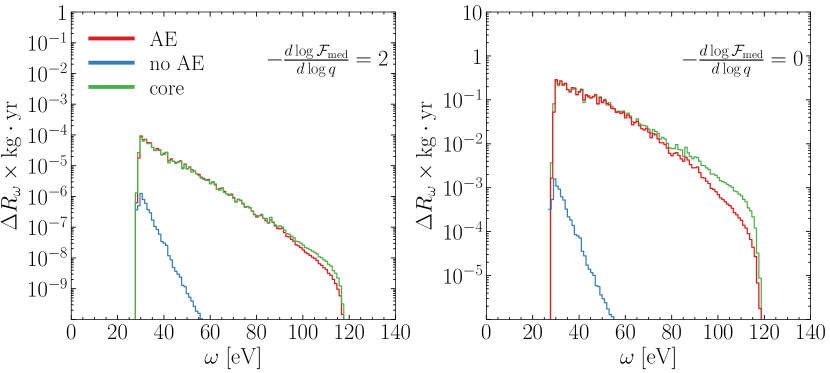
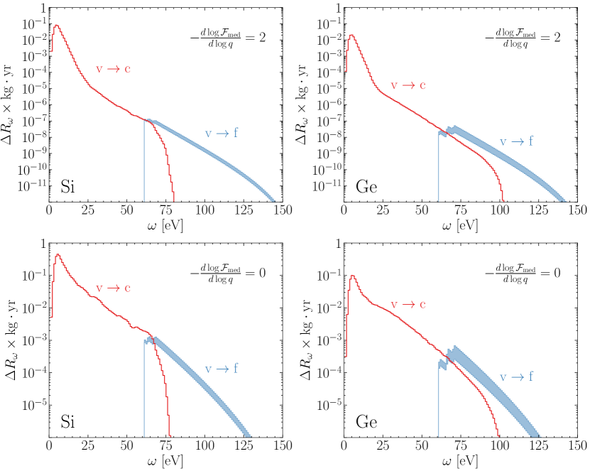
The contribution of core to conduction (cc) transitions to the binned rate, for GeV, can be seen in Fig. 7. In most cases the vc transitions are dominant compared to the cc, but there are two main scenarios where this is not true. First, when the experimental threshold is raised; this excludes the vc transitions and causes the cc contribution to be dominant. For example, consider a Si detector and a DM model with a heavy mediator (bottom left panel of Fig. 7). If the experimental threshold is eV the cc contribution from the 2p states in Si gives the dominant contribution. Second, for a Ge target, and a DM model with a heavy mediator, the 3d states dominate the rate even at the lowest experimental threshold. To understand this in more detail we present Fig. 8 which compares the binned rate taking different modeling approaches for the 3d states in Ge. We see that the large momentum components of the wave function, recovered only after AE reconstruction in the DFT calculation, dominate the rate, which explains why previous works have underestimated the importance of 3d electrons. Meanwhile, we see explicitly at the scattering rate level that the semi-analytic approach accurately reproduces the DFT calculation at low , and extends the latter beyond its cutoff at high , consistent with the observation at the wave function level in Fig. 3.
3.4 Core to Free
The last transition type we consider involves a core electron initial state and a free electron final state. The crystal form factor is most easily obtained by substituting Eqs. (8) and (12) into its definition, Eq. (21):
| (40) |
where the Fourier transform of the RHF Slater type orbital (STO) core wave functions, given in Eq. (10), are known analytically Belkic1989 :
| (41) | ||||
| (42) | ||||
| (43) |
The direct detection rate is then
| (44) |
where , and . We can now shift the variable, and define and . Therefore, and
| (45) |
which is the closest expression to the vacuum matrix element, with just the inclusion of the core wave functions acting as a form factor.
In Fig. 9, we compare the binned rate from the core to conduction (cc) calculation to the core to free (cf) calculation and see a reasonable extrapolation to higher . As with the transition region between vc and vf shown in Fig. 6, we find gives a better match between cc and cf. While the total number of electrons from these transitions is expected to be much less than lower energy transitions, this is the best available calculation for thresholds up to the kinematic limit of .
3.5 In-medium Screening
DM-electron interactions mediated by a dark photon or scalar are screened due to the in-medium mixing between the mediator and the photon. The relevance of screening has been recently emphasized in Ref. Knapen:2021run . The screening factor, , is related to the longitudinal dielectric, , where is the dielectric tensor. It can be computed from in-medium loop diagrams or extracted from optical data. Here we model the dielectric of Si and Ge following Ref. Cappellini1993 :
| (46) |
and . Here, is the static dielectric, is a fitting parameter, is the Thomas-Fermi momentum, and is the plasma frequency. The parameters used for Si and Ge are listed in Table 1, and we plot the dielectric as a function of in Fig. 10.
| Target | ||||
|---|---|---|---|---|
| Si | 11.3 | 1.563 | 16.6 | 4.13 |
| Ge | 14 | 1.563 | 15.2 | 3.99 |
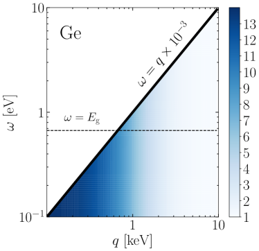
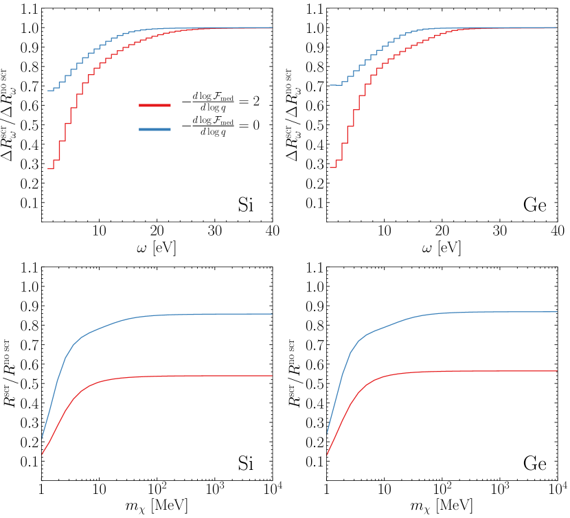
Naively one might expect that the effect of the dielectric is to screen the rate by an factor due to the fact that the static dielectric, , is . However, this is only the value of the dielectric function at , while as and the dielectric approaches unity. Therefore, the effect of the dielectric crucially depends on the region of the kinematic phase space being probed. For a given energy deposition, , the momentum transfer is limited to where is the DM velocity. Therefore, the absolute minimum momentum transfer is , for band gap targets. This is parametrically the same size as the Thomas-Fermi momentum , so the dielectric is expected to slightly deviate from one, which causes only an shift to the scattering rate, as seen in Fig. 11.
4 Projected Sensitivity
We now compile the results from the previous sections to compute the projected sensitivity. We also compare the relative importance of each transition type, and discuss differences between our results and previous calculations in the literature. When there are large differences, it is typically because of the inclusion of AE reconstruction and core states in the calculation. Since AE reconstruction and core states contribute predominantly at higher momentum transfer and energy deposition, we will find the largest differences typically occur for a massive mediator and higher detector threshold, where the effects in some cases can be more than an order of magnitude (especially for Ge). For the case of a massless mediator and lower detection threshold, the differences with previous literature are much smaller and mostly due to the inclusion of in-medium effects.
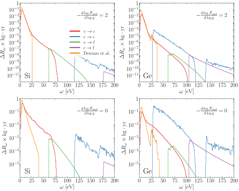
In Fig. 12 we show the contribution to the binned rate from each of the four transition types, for a 1 GeV DM. We see that valence to conduction (vc) has a higher peak than the other three transition types, except for the Ge, heavy mediator case, where core to conduction (cc) has the highest peak. For comparison, Refs. Essig:2015cda ; Derenzo:2016fse compute the valence to conduction rates with DFT, including also the 3d states in Ge, but without AE reconstruction. As expected, we find a lower rate at the lowest energy depositions due to the inclusion of in-medium screening, and a much higher rate at high due to AE reconstruction and inclusion of core states.
The impact of these observations on the reach depends on the energy threshold. Assuming charge readout (e.g. via a CCD), the relevant quantity is the number of electron-hole pairs, , produced in an event. For an energy deposition , this is given by
| (47) |
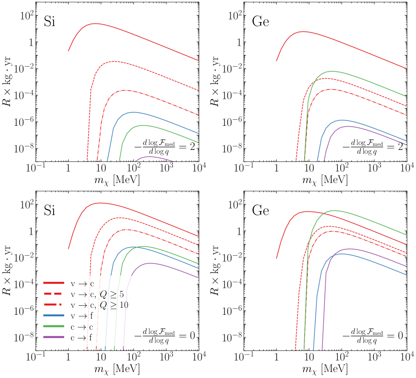
where the values for are eV and eV for Si and Ge respectively. In Fig. 13, we show the total rate as a function of the DM mass, for . The threshold only affects the v c rate, as the other three transition types involve energy depositions corresponding to , and are therefore always fully included. We see that for , the valence to conduction (vc) contribution dominates the total rate with the exception of the Ge, heavy mediator scenario, where core to conduction (cc) is dominant for MeV. Higher thresholds significantly cut out vc contributions in all cases, and render cc more important for Ge, even in the light mediator scenario. For Si, on the other hand, the total rate is still dominated by vc because the core states are much deeper and contribute a lower rate. We also see that vf and cf contributions are subdominant in all cases.
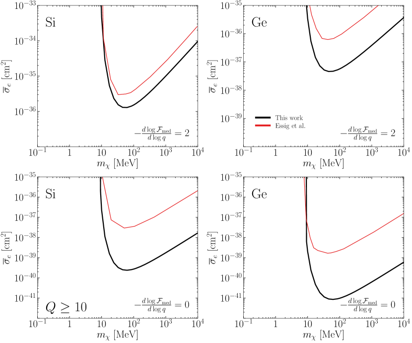
Finally, we present the projected reach on the DM-electron reference cross section in Figs. 14 and 15, for and , respectively. Our new calculation yields several important differences compared to the previous literature, and we discuss them in detail in the following subsection.
4.1 Comparison With Previous Results
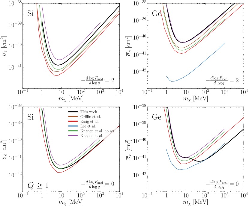
We begin by comparing to our previous work, Ref. Griffin:2019mvc , shown in brown in Fig. 14. We previously restricted our analysis to the light mediator scenario, and , which is relatively unaffected by AE reconstruction effects since the rate is peaked at small energy/momentum transfers, as seen in Fig. 5. The main reason the reach here is weaker is the inclusion of in-medium screening discussed in Sec. 3.5.
Next we compare to Ref. Essig:2015cda , shown in red in Figs. 14 and 15. Those results were computed solely from valence to conduction (vc) transitions. The largest discrepancy is in the high regime scattering off a Ge target via a heavy mediator. This is due to high momentum contributions to the 3d wave functions in Ge. Ref. Essig:2015cda computed the 3d states with DFT without AE reconstruction, which as we saw in Fig. 3 is crucial for recovering the dominant part of the 3d wave functions at high momentum. As discussed in Sec. 2.2, our modeling of 3d electrons in Ge as core states reproduces their DFT-computed wave functions up to the AE reconstruction cutoff, and provides a robust parameterization of higher momentum components. Since the valence states in Ge also contribute an appreciable amount, the results in Fig. 14 only differ by about an order of magnitude. However, the difference is more stark when going to higher thresholds in Fig. 15, which essentially isolates the 3d electrons’ contribution. In the low mass regime the difference is less significant, and primarily due to the inclusion of screening effects. Another difference that is important here is sampling of the 1BZ. Ref. Essig:2015cda used a uniform mesh with extra 27 points chosen by hand close to the center of the 1BZ, whereas here (as well as in Ref. Griffin:2019mvc ) we use a uniform grid. While checking convergence we found our (unscreened) results using a uniform mesh were a closer match to Ref. Essig:2015cda ; generally, increasing the number of points reduces the rate toward convergence, i.e. . This can be seen more directly in the difference between the brown and red lines in the light mediator scenario (as both are computed without screening), and it affects Ge more than Si, as is expected due to the smaller band gap and greater dispersions of nearby bands requiring denser point sampling for convergence.
Ref. Lee:2015qva also computed DM-electron scattering rates in semiconductors, focusing on Ge. The approach taken in that paper was to semi-analytically model the Ge wave functions with the core wave functions (with the same set of RHF STO wave function coefficients tabulated in Ref. Bunge:1993jsz ) and treat the final states as free with a Fermi factor, analogous to the core to free calculation performed here. As we can see from Fig. 14, while for most of the mass range and mediators the estimates are too optimistic due to incorrect modeling of the valence and conduction states, in the high mass region with a heavy mediator (bottom-right panel), where 3d states dominate, their estimates are in good agreement with ours presented here, as expected.
Finally, we discuss the comparison with the most recent work, Ref. Knapen:2021run , which was limited to valence to conduction transitions. To show the effect of screening, we show their projected reach with (purple) and without (green) screening in Fig. 14. Again the largest discrepancy is in the heavy mediator scenario with a Ge target, primarily due to the neglect of the 3d states in Ref. Knapen:2021run . When these are not important, i.e. the low mass regime or a light mediator, we generally find good agreement, with our reach being a bit stronger. Notably this does not seem due to a mis-model of the dielectric, since the effect of screening relative to our previous results, Ref. Griffin:2019mvc , is consistent with their result. We also find that screening has a smaller effect at high masses in the heavy mediator scenario for Si. These small differences are harder to disentangle since they could be due to: 1) different xc-functionals used (PBE and HSE vs. TB09); 2) local field effects which are only partially included here since we assume the screening factor is isotropic; 3) the plane wave expansion parameter, , taken to be eV without AE reconstruction in Ref. Knapen:2021run , vs. 1 keV, AE corrected to 2 keV taken here; 4) DM velocity distribution parameters, studied in detail in Ref. Radick:2020qip , for which Ref. Knapen:2021run assumed kms as opposed to kms chosen here; and 5) Ref. Knapen:2021run took a directionally averaged dielectric, whereas here we only assume isotropy in the screening factor but not the matrix element itself.
5 Conclusions
Dark matter-electron scattering in dielectric crystal targets, especially semiconductors like Si and Ge, are at the forefront of DM direct detection experiments. It is therefore imperative to have accurate theoretical predictions for the excitation rates. In this work, we extended the scattering rate calculation in several key aspects. Much of the focus of previous calculations has been on transitions from valence to conduction bands just across the band gap, which will be accessible to near-future experiments. We performed state-of-the-art DFT calculations for these states, and highlighted the importance of all-electron reconstruction which has been neglected in most previous works. Along with this, we extended the transition rate calculation by explicitly including the contributions from core electrons and additional states more than 60 eV above the band gap using analytic approximations.
We updated the projected reach with our new calculation and found important differences compared to previous results. In particular, we found that in the heavy mediator scenario, 3d electrons in Ge give a dominant contribution to the detection rate for DM heavier than about 30 MeV. Also, the rate can be significantly higher than predicted previously for higher experimental thresholds. This is exciting because new DM parameter space will be within reach even before detectors reach the single electron ionization threshold.
We also release a beta version of EXCEED-DM (available here tanner_trickle_2021_4747696 ) that implements our DM-electron scattering calculation for general crystal targets, and make the electronic wave function data for Si and Ge Trickle2021 , as well as the EXCEED-DM output Trickle2021a , publicly available so our present analysis can be reproduced. We have previously used EXCEED-DM for a target comparison study Griffin:2019mvc , and to study the daily modulation signals that can arise in anisotropic materials Trickle:2019nya . The generality of EXCEED-DM means that potential applications are vast. It can be used to compute detection rates for other target materials (assuming DFT calculations of valence and conduction states are available), and can also be adapted to include additional DM interactions such as in an effective field theory framework similar to the study of atomic ionizations in Ref. Catena:2019gfa (see Ref. Catena:2021qsr for a recent effort in this direction). For momentum-suppressed effective operators, a full calculation in our framework is even more important, as the effects of all-electron reconstruction and core states (overlooked in Ref. Catena:2021qsr ) are generally amplified. Moreover, the differential information that can be obtained from our program facilitates further studies including realistic backgrounds. Details of EXCEED-DM and additional example calculations will be presented in an upcoming publication.
Acknowledgements.
We are grateful to Kyle Bystrom for assistance with pawpyseed, and thank Alex Ganose, Thomas Harrelson, Andrea Mitridate, Michele Papucci and Tien-Tien Yu for helpful discussions. We also thank Rouven Essig and Adrian Soto for early correspondence about QEdark. This material is based upon work supported by the U.S. Department of Energy, Office of Science, Office of High Energy Physics, under Award No. DE-SC0021431 (TT, ZZ, KZ), by a Simons Investigator Award (KZ) and the Quantum Information Science Enabled Discovery (QuantISED) for High Energy Physics (KA2401032). This research used resources of the National Energy Research Scientific Computing Center (NERSC), a U.S. Department of Energy Office of Science User Facility located at Lawrence Berkeley National Laboratory, operated under Contract No. DE-AC02-05CH11231. Some of the computations presented here were conducted on the Caltech High Performance Cluster, partially supported by a grant from the Gordon and Betty Moore Foundation. Work at the Molecular Foundry was supported by the Office of Science, Office of Basic Energy Sciences, of the U.S. Department of Energy under Contract No. DE-AC02-05CH11231.References
- (1) R. Essig, J. Mardon, and T. Volansky, “Direct Detection of Sub-GeV Dark Matter,” Phys. Rev. D85 (2012) 076007, arXiv:1108.5383 [hep-ph].
- (2) P. W. Graham, D. E. Kaplan, S. Rajendran, and M. T. Walters, “Semiconductor Probes of Light Dark Matter,” Phys. Dark Univ. 1 (2012) 32–49, arXiv:1203.2531 [hep-ph].
- (3) S. K. Lee, M. Lisanti, S. Mishra-Sharma, and B. R. Safdi, “Modulation Effects in Dark Matter-Electron Scattering Experiments,” Phys. Rev. D 92 (2015) no. 8, 083517, arXiv:1508.07361 [hep-ph].
- (4) R. Essig, T. Volansky, and T.-T. Yu, “New constraints and prospects for sub-GeV dark matter scattering off electrons in xenon,”Physical Review D 96 (aug, 2017) 043017, arXiv:1703.00910 [hep-ph].
- (5) R. Catena, T. Emken, N. A. Spaldin, and W. Tarantino, “Atomic responses to general dark matter-electron interactions,” Phys. Rev. Res. 2 (2020) no. 3, 033195, arXiv:1912.08204 [hep-ph].
- (6) DarkSide Collaboration, P. Agnes et al., “Constraints on Sub-GeV Dark-Matter–Electron Scattering from the DarkSide-50 Experiment,” Phys. Rev. Lett. 121 (2018) no. 11, 111303, arXiv:1802.06998 [astro-ph.CO].
- (7) XENON Collaboration, E. Aprile et al., “Light Dark Matter Search with Ionization Signals in XENON1T,” Phys. Rev. Lett. 123 (2019) no. 25, 251801, arXiv:1907.11485 [hep-ex].
- (8) XENON Collaboration, E. Aprile et al., “Excess electronic recoil events in XENON1T,” Phys. Rev. D 102 (2020) no. 7, 072004, arXiv:2006.09721 [hep-ex].
- (9) R. Essig, A. Manalaysay, J. Mardon, P. Sorensen, and T. Volansky, “First Direct Detection Limits on sub-GeV Dark Matter from XENON10,” Phys. Rev. Lett. 109 (2012) 021301, arXiv:1206.2644 [astro-ph.CO].
- (10) R. Essig, M. Fernandez-Serra, J. Mardon, A. Soto, T. Volansky, and T.-T. Yu, “Direct Detection of sub-GeV Dark Matter with Semiconductor Targets,” JHEP 05 (2016) 046, arXiv:1509.01598 [hep-ph].
- (11) S. Derenzo, R. Essig, A. Massari, A. Soto, and T.-T. Yu, “Direct Detection of sub-GeV Dark Matter with Scintillating Targets,” Phys. Rev. D 96 (2017) no. 1, 016026, arXiv:1607.01009 [hep-ph].
- (12) Y. Hochberg, T. Lin, and K. M. Zurek, “Absorption of light dark matter in semiconductors,” Phys. Rev. D95 (2017) no. 2, 023013, arXiv:1608.01994 [hep-ph].
- (13) I. M. Bloch, R. Essig, K. Tobioka, T. Volansky, and T.-T. Yu, “Searching for Dark Absorption with Direct Detection Experiments,” JHEP 06 (2017) 087, arXiv:1608.02123 [hep-ph].
- (14) N. A. Kurinsky, T. C. Yu, Y. Hochberg, and B. Cabrera, “Diamond Detectors for Direct Detection of Sub-GeV Dark Matter,” arXiv:1901.07569 [hep-ex].
- (15) T. Trickle, Z. Zhang, K. M. Zurek, K. Inzani, and S. Griffin, “Multi-Channel Direct Detection of Light Dark Matter: Theoretical Framework,” JHEP 03 (2020) 036, arXiv:1910.08092 [hep-ph].
- (16) S. M. Griffin, K. Inzani, T. Trickle, Z. Zhang, and K. M. Zurek, “Multichannel direct detection of light dark matter: Target comparison,” Phys. Rev. D 101 (2020) no. 5, 055004, arXiv:1910.10716 [hep-ph].
- (17) S. M. Griffin, Y. Hochberg, K. Inzani, N. Kurinsky, T. Lin, and T. Chin, “Silicon carbide detectors for sub-GeV dark matter,” Phys. Rev. D 103 (2021) no. 7, 075002, arXiv:2008.08560 [hep-ph].
- (18) P. Du, D. Egana-Ugrinovic, R. Essig, and M. Sholapurkar, “Sources of Low-Energy Events in Low-Threshold Dark Matter Detectors,” arXiv:2011.13939 [hep-ph].
- (19) Y. Hochberg, Y. Zhao, and K. M. Zurek, “Superconducting Detectors for Superlight Dark Matter,” Phys. Rev. Lett. 116 (2016) no. 1, 011301, arXiv:1504.07237 [hep-ph].
- (20) Y. Hochberg, M. Pyle, Y. Zhao, and K. M. Zurek, “Detecting Superlight Dark Matter with Fermi-Degenerate Materials,” JHEP 08 (2016) 057, arXiv:1512.04533 [hep-ph].
- (21) Y. Hochberg, T. Lin, and K. M. Zurek, “Detecting Ultralight Bosonic Dark Matter via Absorption in Superconductors,” Phys. Rev. D94 (2016) no. 1, 015019, arXiv:1604.06800 [hep-ph].
- (22) Y. Hochberg, Y. Kahn, M. Lisanti, K. M. Zurek, A. G. Grushin, R. Ilan, S. M. Griffin, Z.-F. Liu, S. F. Weber, and J. B. Neaton, “Detection of sub-MeV Dark Matter with Three-Dimensional Dirac Materials,” Phys. Rev. D 97 (2018) no. 1, 015004, arXiv:1708.08929 [hep-ph].
- (23) A. Coskuner, A. Mitridate, A. Olivares, and K. M. Zurek, “Directional Dark Matter Detection in Anisotropic Dirac Materials,” arXiv:1909.09170 [hep-ph].
- (24) R. M. Geilhufe, F. Kahlhoefer, and M. W. Winkler, “Dirac Materials for Sub-MeV Dark Matter Detection: New Targets and Improved Formalism,” arXiv:1910.02091 [hep-ph].
- (25) K. Inzani, A. Faghaninia, and S. M. Griffin, “Prediction of tunable spin-orbit gapped materials for dark matter detection,” Physical Review Research 3 (2021) no. 1, 013069.
- (26) DAMIC Collaboration, J. R. T. de Mello Neto et al., “The DAMIC dark matter experiment,” PoS ICRC2015 (2016) 1221, arXiv:1510.02126 [physics.ins-det].
- (27) DAMIC Collaboration, A. Aguilar-Arevalo et al., “Constraints on Light Dark Matter Particles Interacting with Electrons from DAMIC at SNOLAB,” Phys. Rev. Lett. 123 (2019) no. 18, 181802, arXiv:1907.12628 [astro-ph.CO].
- (28) DAMIC, DAMIC-M Collaboration, M. Settimo, “Search for low-mass dark matter with the DAMIC experiment,” in 16th Rencontres du Vietnam: Theory meeting experiment: Particle Astrophysics and Cosmology. 4, 2020. arXiv:2003.09497 [hep-ex].
- (29) SENSEI Collaboration, J. Tiffenberg, M. Sofo-Haro, A. Drlica-Wagner, R. Essig, Y. Guardincerri, S. Holland, T. Volansky, and T.-T. Yu, “Single-electron and single-photon sensitivity with a silicon Skipper CCD,” Phys. Rev. Lett. 119 (2017) no. 13, 131802, arXiv:1706.00028 [physics.ins-det].
- (30) SENSEI Collaboration, M. Crisler, R. Essig, J. Estrada, G. Fernandez, J. Tiffenberg, M. Sofo haro, T. Volansky, and T.-T. Yu, “SENSEI: First Direct-Detection Constraints on sub-GeV Dark Matter from a Surface Run,” Phys. Rev. Lett. 121 (2018) no. 6, 061803, arXiv:1804.00088 [hep-ex].
- (31) SENSEI Collaboration, O. Abramoff et al., “SENSEI: Direct-Detection Constraints on Sub-GeV Dark Matter from a Shallow Underground Run Using a Prototype Skipper-CCD,” Phys. Rev. Lett. 122 (2019) no. 16, 161801, arXiv:1901.10478 [hep-ex].
- (32) SENSEI Collaboration, L. Barak et al., “SENSEI: Direct-Detection Results on sub-GeV Dark Matter from a New Skipper-CCD,” Phys. Rev. Lett. 125 (2020) no. 17, 171802, arXiv:2004.11378 [astro-ph.CO].
- (33) SuperCDMS Collaboration, R. Agnese et al., “Search for Low-Mass Weakly Interacting Massive Particles with SuperCDMS,” Phys. Rev. Lett. 112 (2014) no. 24, 241302, arXiv:1402.7137 [hep-ex].
- (34) SuperCDMS Collaboration, R. Agnese et al., “New Results from the Search for Low-Mass Weakly Interacting Massive Particles with the CDMS Low Ionization Threshold Experiment,” Phys. Rev. Lett. 116 (2016) no. 7, 071301, arXiv:1509.02448 [astro-ph.CO].
- (35) SuperCDMS Collaboration, R. Agnese et al., “Projected Sensitivity of the SuperCDMS SNOLAB experiment,”Phys. Rev. D95 (Apr, 2017) 082002, arXiv:1610.00006 [physics.ins-det]. https://link.aps.org/doi/10.1103/PhysRevD.95.082002.
- (36) SuperCDMS Collaboration, R. Agnese et al., “Low-mass dark matter search with CDMSlite,” Phys. Rev. D 97 (2018) no. 2, 022002, arXiv:1707.01632 [astro-ph.CO].
- (37) SuperCDMS Collaboration, R. Agnese et al., “First dark matter constraints from a SuperCDMS single-charge sensitive detector,”Physical Review Letters 121 (aug, 2018) 051301, arXiv:1804.10697 [hep-ex]. [Erratum: Phys.Rev.Lett. 122, 069901 (2019)].
- (38) SuperCDMS Collaboration, R. Agnese et al., “Search for Low-Mass Dark Matter with CDMSlite Using a Profile Likelihood Fit,” Phys. Rev. D 99 (2019) no. 6, 062001, arXiv:1808.09098 [astro-ph.CO].
- (39) SuperCDMS Collaboration, D. W. Amaral et al., “Constraints on low-mass, relic dark matter candidates from a surface-operated SuperCDMS single-charge sensitive detector,” Phys. Rev. D 102 (2020) no. 9, 091101, arXiv:2005.14067 [hep-ex].
- (40) EDELWEISS Collaboration, E. Armengaud et al., “Searches for electron interactions induced by new physics in the EDELWEISS-III Germanium bolometers,” Phys. Rev. D 98 (2018) no. 8, 082004, arXiv:1808.02340 [hep-ex].
- (41) EDELWEISS Collaboration, E. Armengaud et al., “Searching for low-mass dark matter particles with a massive Ge bolometer operated above-ground,” Phys. Rev. D 99 (2019) no. 8, 082003, arXiv:1901.03588 [astro-ph.GA].
- (42) EDELWEISS Collaboration, Q. Arnaud et al., “First germanium-based constraints on sub-MeV Dark Matter with the EDELWEISS experiment,” Phys. Rev. Lett. 125 (2020) no. 14, 141301, arXiv:2003.01046 [astro-ph.GA].
- (43) C. Bunge, J. Barrientos, and A. Bunge, “Roothaan-Hartree-Fock Ground-State Atomic Wave Functions: Slater-Type Orbital Expansions and Expectation Values for Z = 2-54,” Atom. Data Nucl. Data Tabl. 53 (1993) 113–162.
- (44) P. Giannozzi et al., “Quantum espresso: a modular and open-source software project for quantum simulations of materials,” Journal of Physics: Condensed Matter 21 (2009) no. 39, 395502 (19pp). http://www.quantum-espresso.org.
- (45) P. Giannozzi et al., “Advanced capabilities for materials modelling with quantum espresso,” Journal of Physics: Condensed Matter 29 (2017) no. 46, 465901. http://stacks.iop.org/0953-8984/29/i=46/a=465901.
- (46) P. Giannozzi et al., “Quantum espresso toward the exascale,” The Journal of Chemical Physics 152 (2020) no. 15, 154105, https://doi.org/10.1063/5.0005082. https://doi.org/10.1063/5.0005082.
- (47) Y. Hochberg, Y. Kahn, N. Kurinsky, B. V. Lehmann, T. C. Yu, and K. K. Berggren, “Determining Dark Matter-Electron Scattering Rates from the Dielectric Function,” arXiv:2101.08263 [hep-ph].
- (48) S. Knapen, J. Kozaczuk, and T. Lin, “Dark matter-electron scattering in dielectrics,” arXiv:2101.08275 [hep-ph].
- (49) S. Knapen, J. Kozaczuk, and T. Lin, “DarkELF: A python package for dark matter scattering in dielectric targets,” arXiv:2104.12786 [hep-ph].
- (50) Z.-L. Liang, L. Zhang, P. Zhang, and F. Zheng, “The wavefunction reconstruction effects in calculation of DM-induced electronic transition in semiconductor targets,” JHEP 01 (2019) 149, arXiv:1810.13394 [cond-mat.mtrl-sci].
- (51) S. Griffin, S. Knapen, T. Lin, and K. M. Zurek, “Directional Detection of Light Dark Matter with Polar Materials,” Phys. Rev. D 98 (2018) no. 11, 115034, arXiv:1807.10291 [hep-ph].
- (52) A. Coskuner, T. Trickle, Z. Zhang, and K. M. Zurek, “Directional Detectability of Dark Matter With Single Phonon Excitations: Target Comparison,” arXiv:2102.09567 [hep-ph].
- (53) T. Trickle, “tanner-trickle/EXCEED-DM: EXCEED-DM-v0.1.0,” Zenodo, May, 2021. https://doi.org/10.5281/zenodo.4747696.
- (54) T. Trickle, “EXCEED-DM: DFT-computed electronic wave functions for Si and Ge,” Zenodo, 2021.
- (55) T. Trickle, “EXCEED-DM: Calculated Scattering Rate Data for Si and Ge,” Zenodo, 2021.
- (56) P. Hohenberg and W. Kohn, “Inhomogeneous Electron Gas,” Phys. Rev. 136 (1964) B864–B871.
- (57) R. M. Martin, Electronic structure: basic theory and practical methods. Cambridge university press, 2020.
- (58) W. Kohn and L. J. Sham, “Self-Consistent Equations Including Exchange and Correlation Effects,” Phys. Rev. 140 (1965) A1133–A1138.
- (59) J. P. Perdew, K. Burke, and M. Ernzerhof, “Generalized Gradient Approximation Made Simple,” Physical Review Letters 77 (1996) no. 18, 3865–3868. http://link.aps.org/doi/10.1103/PhysRevLett.77.3865.
- (60) J. Heyd, G. E. Scuseria, and M. Ernzerhof, “Hybrid functionals based on a screened Coulomb potential,” Journal of Chemical Physics 118 (2003) no. 18, 8207–8215.
- (61) J. Heyd, G. E. Scuseria, and M. Ernzerhof, “Erratum: Hybrid functionals based on a screened Coulomb potential (Journal of Chemical Physics (2003) 118 (8207)),” Journal of Chemical Physics 124 (2006) no. 21, . https://doi.org/10.1063/1.2204597.
- (62) P. Blöchl, “Projector augmented-wave method,” Physical Review B 50 (1994) no. 24, 17953–17979.
- (63) G. Kresse and D. Joubert, “From ultrasoft pseudopotentials to the projector augmented-wave method,” Physical Review B 59 (1999) 1758–1775.
- (64) G. Kresse and J. Hafner, “Ab initio molecular dynamics for liquid metals,” Physical Review B 47 (1993) 558–561.
- (65) G. Kresse and J. Hafner, “Ab initio molecular-dynamics simulation of the liquid-metal–amorphous-semiconductor transition in germanium,” Physical Review B 49 (1994) no. 20, 14251–14269. http://link.aps.org/doi/10.1103/PhysRevB.49.14251.
- (66) G. Kresse and J. Furthmüller, “Efficiency of ab initio total energy calculations for metals and semiconductors using a plane-wave basis set,” Computational Materials Science 6 (1996) 15–50.
- (67) G. Kresse and J. Furthmüller, “Efficient iterative schemes for ab initio total-energy calculations using a plane-wave basis set,” Physical Review B 54 (1996) 11169–11186. http://link.aps.org/doi/10.1103/PhysRevB.54.11169.
- (68) C. Rostgaard, “The projector augmented-wave method,” arXiv:0910.1921 [cond-mat.mtrl-sci].
- (69) K. Bystrom, D. Broberg, S. Dwaraknath, K. A. Persson, and M. Asta, “Pawpyseed: Perturbation-extrapolation band shifting corrections for point defect calculations,”arXiv e-prints (Apr, 2019) arXiv:1904.11572, arXiv:1904.11572 [cond-mat.mtrl-sci].
- (70) G. H. S. E. U. Condon, The Theory of Atomic Spectra. Cambridge University Press, January, 1935. https://www.ebook.de/de/product/4287067/e_u_condon_george_h_shortley_the_theory_of_atomic_spectra.html.
- (71) D. Belkić and H. S. Taylor, “A unified formula for the fourier transform of slater-type orbitals,”Physica Scripta 39 (feb, 1989) 226–229.
- (72) G. Cappellini, R. D. Sole, L. Reining, and F. Bechstedt, “Model dielectric function for semiconductors,”Physical Review B 47 (apr, 1993) 9892–9895.
- (73) A. Radick, A.-M. Taki, and T.-T. Yu, “Dependence of Dark Matter - Electron Scattering on the Galactic Dark Matter Velocity Distribution,” JCAP 02 (2021) 004, arXiv:2011.02493 [hep-ph].
- (74) R. Catena, T. Emken, M. Matas, N. A. Spaldin, and E. Urdshals, “Crystal responses to general dark matter-electron interactions,” arXiv:2105.02233 [hep-ph].