Analog Neural Computing with Super-resolution Memristor Crossbars
Abstract
Memristor crossbar arrays are used in a wide range of in-memory and neuromorphic computing applications. However, memristor devices suffer from non-idealities that result in the variability of conductive states, making programming them to a desired analog conductance value extremely difficult as the device ages. In theory, memristors can be a nonlinear programmable analog resistor with memory properties that can take infinite resistive states. In practice, such memristors are hard to make, and in a crossbar, it is confined to a limited set of stable conductance values. The number of conductance levels available for a node in the crossbar is defined as the crossbar’s resolution. This paper presents a technique to improve the resolution by building a super-resolution memristor crossbar with nodes having multiple memristors to generate -simplicial sequence of unique conductance values. The wider the range and number of conductance values, the higher the crossbar’s resolution. This is particularly useful in building analog neural network (ANN) layers, which are proven to be one of the go-to approaches for forming a neural network layer in implementing neuromorphic computations.
Index Terms:
Crossbar, analog neural network, multiply and accumulate, analog neural acceleratorI Introduction
In the design of neural network accelerators, multiply and accumulate (MAC)[1, 2, 3] block emulates the weighted summation of inputs in a neural network layer. Every layer of the neural network requires the MAC operation. The neural network accelerators [4, 5, 6, 7, 8] are used in the edge AI computing domain to make sensing smarter and data processing energy efficient. The offloading of neural network computing from high-performance computers to edge AI processors improves energy efficiency, and reduces costs, and bandwidth requirements.
The MAC block can be implemented with digital or analog circuits. In a digital-only approach, the inputs, and weights are stored in a binary form. Such a system is most suitable if using binary memory arrays, such as SRAM or DRAM through in-memory computing [9, 10, 11]. In an analog approach, the MAC operation uses weights and/or inputs in analog forms, such as when implementing using a floating gate or ReRAM array[12]. The most popular approach to building MAC in the analog domain is the crossbar architecture[13, 14].
In a crossbar architecture, the crossbar nodes can be accessed by row or column lines. The rows are used to apply the input signals, while the columns are used to read the output signals. The crossbar nodes of our interest have a programmable conductance. When a voltage is applied to the crossbar node, the column’s output current represents the weighted summation of inputs, or rather the MAC operation.
A popular conductance device for building a crossbar node is the memristor[15, 16]. Several devices claim to have similar properties as memristors[17, 18, 19, 20]. The neural network applications of memristors in the crossbar require the mapping of neural network weights to the crossbar nodes’ conductance values. This mapping of weight is only possible on a single memristor having infinite conductance levels. Because memristors with precise and stable infinite conductance levels are currently not practically feasible, encoding schemes need to be applied.
One approach is to encode the weights as a binary sequence or to discretize the weights to fit the available memristor conductance levels [21, 22]. This limitation of weight resolutions determines the overall design of the MAC implementation, and thereby the neural network performance. Subsequent to the resolution limitation, the memristor is also sensitive to process variations and device-to-device variabilities, which leads to conductance variability [23, 24, 25, 26, 27]. The endurance and aging of the device play an important role in the reliability of the crossbar, and often make the circuit designers work difficult [28].
Connecting memristors in parallel using PCM devices [29, 30] increases the reliability and fault tolerance of synapses. Likewise, ReRAM based parallel memristors were used in [31] to reduce the impact of stochasticity and nonlinearity. Whereas, in this paper, we present the theory of combining the memristors within a crossbar without modifying the widely used crossbar structures as a fundamental technique to generalise crossbar for any precision multiply and accumulate operation. A practical approach to improve the conductance resolution of crossbar arrays is proposed. The main contributions of this work include (1) a super-resolution crossbar design, (2) theory of estimating the conductance levels and (3) implication on the practical design of analog neural networks.
This paper is organized into the following sections: Section II gives a background on crossbars that inspire analog computing, Section III provides the details of the proposed design approach and supporting theory, Section IV reports the results and related discussion. Finally, Section V provides the summary of the paper.
II Background
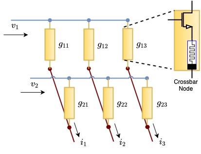
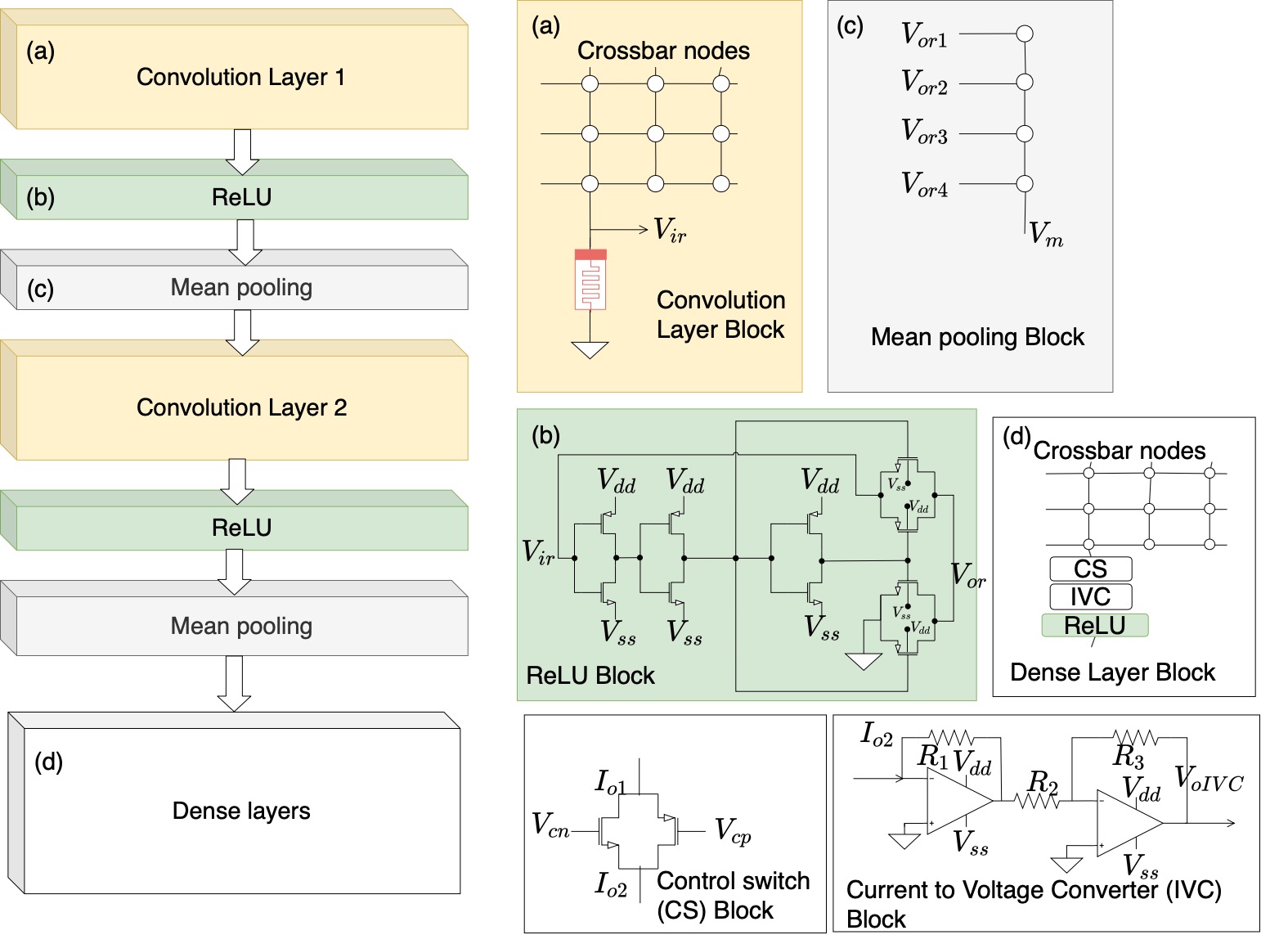
The crossbar arrangement of memristors in 1T1M configuration is shown in Fig. 1. The transistor switch enables or disables the column-wise memristor nodes. In this example, the inputs () are applied across the rows of the crossbar, and outputs () measured at the columns of the crossbar. Each memristor has a conductance , where are the coordinates of the crossbar nodes. The output currents indicate the weighted summation of inputs. The output currents from the th neuron (column of crossbar) can be represented as , with number of inputs (number of rows in the crossbar), representing a dot-product or MAC operation or vector-multiplication (VMM) [32, 33, 34, 35, 36, 37, 38, 39, 40]. In a neural network implementation, this weighted summation of inputs represents a neuron representation without activation function. In the crossbar, bias can be included by adding additional input line. The memristor programming and line selection is done using a selector switch in series with the memristor as shown in Fig. 1. The selector switch enables the memristor node by applying a gate voltage sufficiently higher than the threshold voltage to drive the transistor switch to ON mode. In analog neural networks, the are weight variables that can take continuous values. In most practical hardware implementations, the is a discrete variable having limited set of values. As memristors have high readout speeds in crossbar, the MAC operations can perform analog numerical computations [41]. An example is the Phase Change Memory based memristor crossbar to solve linear system of equations using iterative refinement algorithm in a mixed-signal architecture. Such a system showed computational complexity of for an D D matrix, compared to in traditional numerical computation algorithms [42].
The crossbars’ reading and writing require additional circuits specific to the neural network architecture. In many neural networks, the weights can be positive and negative. To implement such a system, each synaptic column is represented as two distinct column lines, thereby doubling up the number of memristors required. The negative and positive signs are achieved by splitting the conductance components as positive and negative along two crossbar columns (say positive and negative column), which reflects as . Here, the weights of the neuron , where , and are conductance of memristor nodes in positive and negative columns, respectively, while current difference is realised with a sense amplifier having a current difference circuit.
The readout circuits comprises sense amplifiers and data converters [43]. There are two main possibilities in processing the current outputs. They can be passed through an analog implementation of the activation function followed by the next neural crossbar layer. Alternatively, the output currents can be digitally encoded using a data converter, followed by activation function computation and the next layer of input. In an analog-only approach, the design of sense amplifier and activation function becomes challenging, as they are power-hungry, although it can be area efficient. In digital-only implementations, the power is on the lower end, but they become area inefficient due to data converters and multiplexing units.
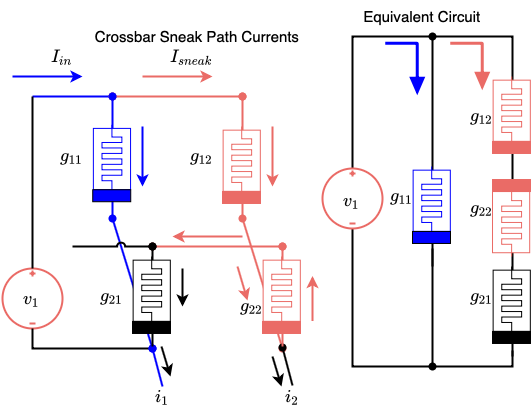
In Fig. 2 example, it can be noted that each column is assumed to be coupled to a sense amplifier. If the column with is not coupled to a sense amplifier, all current in such case will go to . The sneak path currents [44, 45, 46, 47, 48, 49, 50] in the crossbar can be controlled by serial reads, making the crossbar reads slower. In serial read, one column in the crossbar is enabled at a time and the output currents are read along the column. In parallel read, multiple columns in the crossbar are enabled and the output currents are read along the enabled columns in parallel simultaneously. A parallel read is faster, but have more current errors. Smaller crossbars will have a fewer paths in the crossbar to induce sneak path errors. Keeping the crossbar size smaller also lowers the line capacitance and signal integrity issues.
Increasing the crossbar size is required for building large neural networks. One way to get around this problem is using modular crossbar arrays or crossbar tiles [51, 52]. The current summation can be split into several sub-currents by splitting the large crossbar into a set of smaller crossbars followed by summing the output currents. As smaller crossbar will have smaller leakage currents, lower sneak-path currents due to the use of multiple crossbars to represent larger crossbars, and parasitic errors.
III Super-resolution Crossbar Nodes
In a memristor crossbar, any undesired change node conductance will lead to errors in output column current. Ideal memristors can be programmed to an infinite number of stable conductance values. However, practical memristors can be programmed to only a limited number of stable conductance values. The number of stable conductance values is defined as conductance levels. If the conductance of the memristor is limited to levels, i.e., number of conductance values per device, many optimal weights of the neural network will become difficult to translate directly to hardware. One approach around this is to encode the weights with a set of memristor devices in the crossbar.
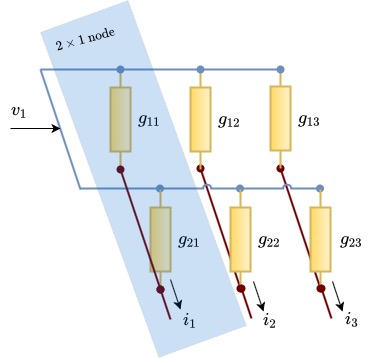
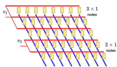
In the proposed approach, multiple rows are tied to a single input, as shown in Fig. 3, enhancing the number of conductance levels per node and increase the overall resolution of the crossbar. Suppose each memristor have only two states, i.e. , then the weights are considered to be binary. Now, when we connect two rows for a single input, the overall conductance will be the summation of the two conductance, which means it can take at most any of the three unique conductance values (see Table I). The occurrence of conductance combinations can be expressed in a polynomial form. If we represent, and as the symbolic occurrence of and , respectively, a node with two memristors can be expressed as , where translates to , translates to , and translates to . Here, and are indicative of the number of conductance levels per memristor, and the power of 2 represents the number of memristors.
| Memristor 1 | Memristor 2 | Overall conductance |
Extending the idea to memristors, this can be represented as , leading to having binomial properties for finding the unique coefficients. This indicates that the number of coefficients follows the simplicial polytopic numbers sequences.
Theorem 1.
A combination of bi-level conductance memristors in parallel for creating the super-resolution crossbar conductance node follows unique conductances () of 2,3,4..+1 by encoding 1-simplicial number patterns. The increase in enables the conversion of binary conductance nodes to analog discrete conductance nodes in a crossbar.
Proof: Table II shows the number of memristors and corresponding unique conductance per node. Let’s denote the unique conductance set for bi-level memristor nodes with as . This sequence are part of simplicial sequence if it encodes the 1-simplicial number properties. Here, we can rewrite,
, for, and .
Suppose, represents the sum of numbers in the sequence and represents the sum of numbers in the sequence . Here, , and therefore, for . For example, for , ; for , , and so forth, with for , for , and so forth. The conductance with different memristor numbers are given in Table II.
The sum of the sequence validates the existence of 1-simplicial sequence or the Triangular gnomon (linear) number sequence.
We can also further observe additional relations between and , for computing the value of given or , and vice versa:
(1) ,
(2) ,
(3) .
Given that validates for being 1-simplicial numbers and as it is encoded in ; we can say that for encodes 1-simplicial numbers. This proves Theorem 1 on the existence of 1-simplicial number patterns in the unique conductance set by combining bi-level memristors.
Theorem 1 has implications in the design and use of binary crossbar array. Any binary crossbar array can be transformed into an analog crossbar array using the proposed super-resolution principle. In other words, the memristors with two states can create nodes with several conductance levels by adding more memristors in parallel. As shown in Table II, a node with memristors can achieve conductance values. Because we use 10 rows of the crossbar to represent single input, i.e., ten memristors per input node, with each having a binary conductance state, we can obtain 11 unique conductive states, which in itself does not show as a major advantage. However, with the increasing number of conductive states per memristor, the scenario significantly changes. For example, two memristors in a node with each memristor having two conductive states results in unique conductance () that follow 2-dimensional simplicial number sequence as shown in Table III.
| Number of memristors | Unique conductance |
| 1 | 2 |
| 2 | 3 |
| 3 | 4 |
| 4 | 5 |
| .. | .. |
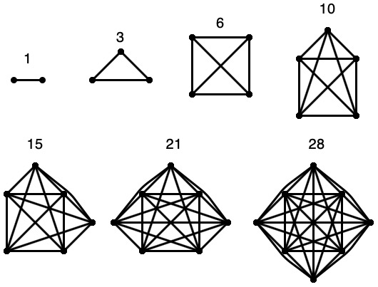
The simplicial polytopic numbers belong to the broad class of figurate numbers that are -dimensional simplex for each dimension in the Euclidean space , with . In algebraic topology, the - simplex is a -dimensional polytope and is a convex hull of vertices. They can be visualized as a generalization of the triangle to any arbitrary dimension, connected to the coefficients of multi-nominal expressions. These topological representations lay the foundations of the simplicial polytopic numbers.
The number of unique conductance combinations follows multi-nominal expressions and can be represented as simplicial numbers. 2-simplicial numbers originate out of 2-simplex having 3 vertices representative of the triangle (the 3 1-cell, with 3 segments as facets). Figure 4 shows the visualisation of the 2-simplicial numbers derived by counting the number of segments (or edges) of triangular shapes with an increasing number of vertices. Counting the number of segments in each shape gives the sequence, , which forms the 2-simplicial numbers. Likewise, 3-simplicial numbers originate out of 3-simplex having 4-vertices representative of the tetrahedron (the 4 2-cell, with 4 faces as facets). In general, -simplicial numbers originate out of -simplex having vertices representative of the triangle (the -cell, with segments as facets).
Theorem 2.
The -level conductance memristors super-resolution crossbar conductance node follows an -dimensional simplicial number sequence. Increasing irrespective of results in an increase in , such that .
Proof: Table III shows the set of unique conductance () following simplicial numbers for nodes with number of memristors. The conductance values for , for is shown in Table IV, which follows the -simplicial number sequences. For a simplicial sequence, the th simplicial -polytopic number can be calculated as: . Replacing, with , and with , we find that the values of in Table IV is same as that obtained by applying equation for , as , and . Here, we observe that is a function of and , with:
…….
This implies that, =+, is the recurrence relation for th simplicial -polytopic numbers. Applying the equation for and replacing with , and with , the unique number of conductance sequence from a node with memristors can be then written as . Here, can be considered as the dimension of the regular convex simplicial polytope number sequence, while is the number of memristors per node as the number of nondegenerate layered simplices. For any given value of , suppose the memristor has levels, then the unique number of levels becomes , which makes for , and for . This implies that for any value of .
| Number of memristors () | Number of levels () | Unique conductance () | Sequence type |
|---|---|---|---|
| 1 | 1-simplicial numbers | ||
| 2 | 2-simplicial numbers | ||
| 3 | 3-simplicial numbers | ||
| 4 | 4-simplicial numbers | ||
| 5 | 5-simplicial numbers | ||
| 6 | 6-simplicial numbers | ||
| 7 | 7-simplicial numbers | ||
| 8 | 8-simplicial numbers |
| 1-M | 2-M | 3-M | ||||
|---|---|---|---|---|---|---|
| Conductance value | Conductance value | Conductance value | ||||
| 1 | 1 | 1 | 1 | |||
| 2 | 2 | 3 | 4 | |||
| 3 | 3 | 6 | 10 | |||

In such a generalization, both the number of conductance levels and memristors can be increased. Currently, there are memristors that can have more than 100 conductance levels [53]. However, most of the memristor devices have only very few stable conductance levels that are easily programmed under the influence of integrated circuit parasitics and aging. To build analog crossbar arrays that can map weights at high accuracy and precision, it must have a higher number of levels.
The proposed approach, when extended to include the impact of a higher number of conductance levels per device, implies a higher number of possible conductance per node. Table III shows the generalization of this scenario. It is observed that the unique conductance per node for a given number of memristors follows -simplicial numbers. With memristors having even 3 stable levels, increasing the number of memristors per node can lead to a large number of conductance levels per node as seen in Tables III and IV. As the number of levels per memristor increases, fewer memristors are required to achieve a high number of levels per node. For example, a node made up of 8 memristors, each having 8 levels, will result in 6435 unique conductance per node.
III-A Illustrative Example
Table IV shows the conductance calculations for crossbar nodes made up of one memristor (1-M), two memristors (2-M), and three memristors (3-M). Each memristor has conductance levels. The for 1-M follows the set {1,2,3..}, 2-M follows the set {1,3,6..} and 3-M follows the set {1,4,10..}. Thus, the -M node follows the simplicial number sequence , where is the number of memristors per node. Figure 5 shows the programming scheme and using the superresolution nodes in the inference stage. The programming of the memristors in each node is achieved by applying the SET and RESET cycles of pulses. For the programming stage, the desired conductance states and for the 1T1M memristor node can be obtained by repeated SET and RESET cycles, as shown in Fig. 5(b). The switch over between the SET and RESET operations use the switching logic shown in Fig. 5(c). The voltage pulses induce low potential difference during read (or inference or verify operation), high positive potential difference during program operations, and negative potential difference during the erase operation across the memristor. During the inference, the crossbar does not need any modification, and superresolution nodes can be formed by feeding the same voltage to and 1T1R nodes to form sized superresolution node, as shown in Fig. 5(a).
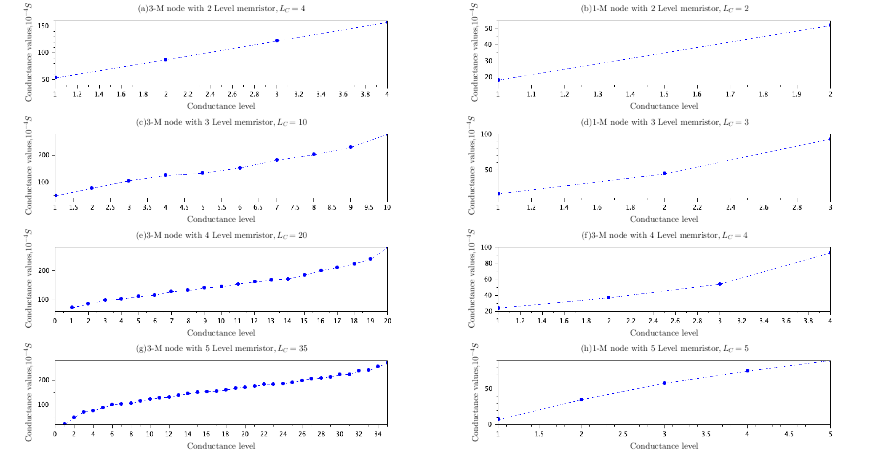
Figure 6 shows the example simulation of conductance level distribution resulting from a 3-M node compared with a 1-M node. The 3-M nodes built with memristors having 2, 3, 4, and 5 unique conductance levels can result in 4, 10, 20, and 35 unique conductance levels, respectively. In this example, the memristors’ conductance levels are randomly assigned to a stable value that the individual memristor can be programmed. The resulting 3-M node shows a higher number of stabilized and unique conductance values. Therefore, the 3-M based crossbar can have a higher weight resolution in a neural network than 1-M nodes. The conductance drift due to aging in 1-M nodes can result in loss of conductance levels that cannot be recovered quickly. Even if one of the memristor loss levels in a 3-M, the available conductance levels () in the remaining two memristors can still result in large values of for the superresolution nodes. The example also shows that individual memristors in a 3-M node can easily program the states to a few stable states distributed in any fashion. The resulting conductance space will be large, allowing for more considerable weight precision.
Programming sequence
An example sequence to program the conductance values of the 3-M node, using three memristors each having four levels is shown in Table V. The node conductance can be mapped to the weights in the neural network application or general in-memory computing applications using a lookup approach. Suppose a weight of 0.3 is mapped to the conductance of 40 , the three memristors in the 3-M node are required to be programmed to the combination without following the sequenced order 15, 15, and 10 values. The intermediate weight values such as 0.33 are rounded off to 0.3 by the nearest distance search and subsequently programmed to the value from the lookup table, in Table V. In contrast, a 1-M node with four levels would have resulted in a significant loss of weight precision as many intermediate levels are missed out. Through this approach, the complexity of programming crossbar nodes to obtain high-resolution weights substantially reduces, as fewer levels are often easier to program and are more reliable to achieve. In addition, the super-resolution nodes are formed by a parallel or series combination of memristors, depending on the ease of programming conductance or resistance of individual memristors, respectively. More details on programming memristor based on the resistance or conductance are included in the Supplementary material.
| 3-M node conductance() | 3-M node conductance() | ||
| 10 | 10 | 10 | 30 |
| 15 | 10 | 10 | 35 |
| 15 | 15 | 10 | 40 |
| 15 | 15 | 15 | 45 |
| 29 | 10 | 10 | 49 |
| 29 | 15 | 10 | 54 |
| 29 | 15 | 15 | 59 |
| 29 | 29 | 10 | 69 |
| 29 | 29 | 15 | 74 |
| 29 | 29 | 29 | 88 |
| 1000 | 10 | 10 | 1020 |
| 1000 | 15 | 10 | 1025 |
| 1000 | 15 | 15 | 1030 |
| 1000 | 29 | 10 | 1039 |
| 1000 | 29 | 15 | 1044 |
| 1000 | 29 | 29 | 1059 |
| 1000 | 1000 | 10 | 2010 |
| 1000 | 1000 | 15 | 2015 |
| 1000 | 1000 | 29 | 2029 |
| 1000 | 1000 | 1000 | 3000 |
Case of 3D crossbar
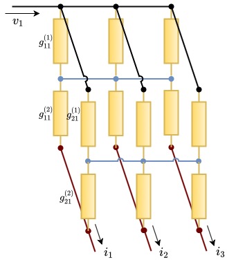
As an extension, the resistance range can be further increased using a 3D crossbar array. In the example shown in Fig. 7, the top and bottom layer conductances are denoted as , and , respectively. Because each node is a parallel combination of two memristors connected in series across two layers, current . Each memristor node has a selector switch. When current is read, the memristor nodes in columns and are kept to OFF state. Hence, will be in series to In general, the read out currents from any one column is given as, , with the equivalent node conductance as follows:
| (1) |
Such 3D nodes can further extend the number of levels without significantly increasing the area on-chip. The different configurations and possibilities with the 3D crossbar array are a topic for future study.
IV Results and Discussion
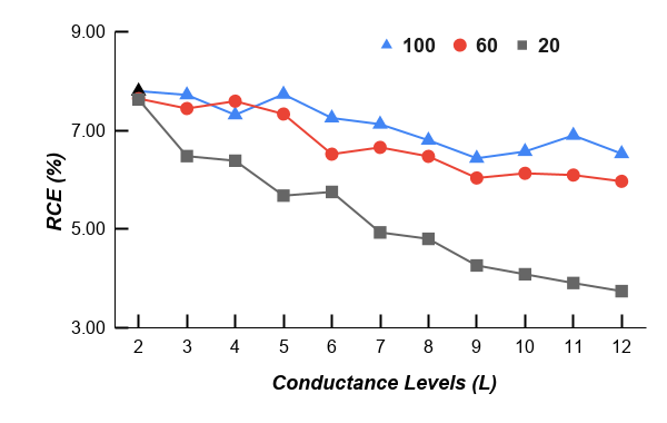
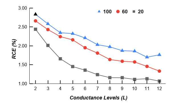
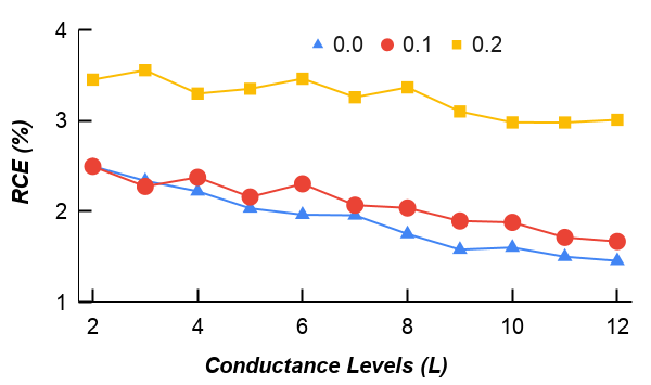
The crossbars are used in a range of applications, mainly, in building neural network accelerators. To check the impact of the number of conductance per node on the overall performance of the crossbar, we take a crossbar array with 1010 nodes. The conductance programming is performed using an adaptive program and verify approach [54]. The output currents are read from the columns for the different memristors and conductance levels per node. Throughout the paper, unless mentioned otherwise, random current read errors are added as a Gaussian distribution with mean zero and standard deviation as 10% of ideal read currents to account for the non-idealities of the sensing circuits connected to the crossbar. Figure 8 shows the relative output current error (RCE) in percentage, calculated as , where is the output current obtained when nodes have infinite number of conductance levels, and is the output current obtained with a limited number of conductance levels.
Precision
The precision of the weights mapping to crossbar nodes is an important factor that determines the accuracy of analog dot product computations. It can be observed from Fig. 8 that as the number of memristor per node increases, the current error decreases. The increase in along with increase in results in a large increase in , as shown in Table III. As increases, i.e. for larger value of and , the current error tends to zero. The memristors in the superresolution crossbar are connected in parallel and the current readout from the nodes will be the weighted average of the input voltage, i.e. , where input voltage to a node with memristors each having its own conductance . Suppose there is a variation in one of the conductance values say in the th memristor i.e. , with being the offset from the true value, then we can write, or . Thus the variations, i.e. , will have less impact on the overall current as the value of increases.
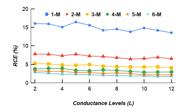
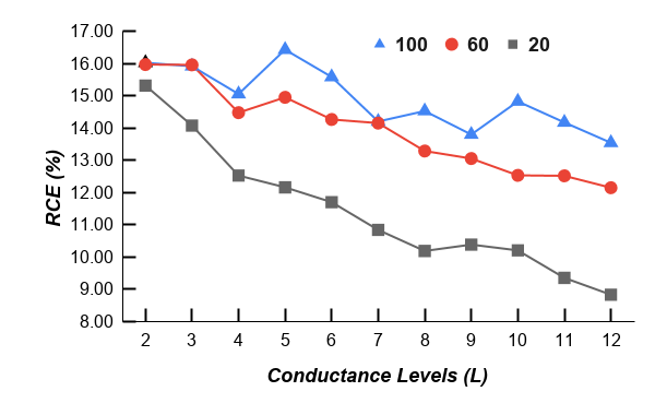
Figure 9 shows the average relative current errors (RCE), with changes in ratio of memristor relative to the node size. The larger the ratio, the larger the RCE values irrespective of the node size. However, as the number of memristors increases in the node, the RCE values drastically reduce irrespective of the changes in ratio, indicating the crossbar superresolution’s usefulness.
Area and power
Each memristor has one selector transistor switch. Irrespective of the node size, i.e., nodes with memristor T-M, the interface circuits required at the output of the analog neural network crossbar remain the same. If we assume the area occupied by interface circuits connected to each of the crossbar column to be , and the area of each 1T1M node to be , then the minimum total area for implementing one layer of a neural network will be , where is the number of columns in the crossbar, is the number of nodes in a column, and is the number of memristors per node. In analog neural network implementations [55], , for example, in a 180 nm CMOS technology111The 180 nm CMOS node used is for demonstrative purpose only. It is possible to use lower node sizes such as 22 nm or lower FinFETs [56] node sizes for reducing the area and power requirements in practical applications. For memristors, we used Knowm MSS (Multi-Stable Switch) memristor model and WOx device parameters [57]., the interface circuits to each column of the crossbar consists of I-V converter block, Opamp buffer, and ReLU block, occupying areas of 96.714 m2, 44.712m2, and 23.659m2, respectively, as shown in Fig. 10222Here, the ReLU PMOS has W/L=0.36/0.18, and ReLU NMOS has W/L=1/0.18. Switch transistor sizes are 5/0.18 (PMOS), and 20/0.18(NMOS), and feedback resistors . The single 1T1M memristor node occupies an area of 0.14m2. For a super-resolution crossbar, with 8T8M nodes, the minimum areas are , and , where , , . Alternatively, if we use a classical crossbar, 1T1M nodes spread across 8 columns, the equivalent crossbar will have a size of , with minimum areas of , and , where , , and . In addition, as the lower and upper limits of resistance values in the crossbar node (i.e., and limits) does not change, and reverse leakage currents in the transistors are relatively lower than the forward currents in the memristor, the net maximum current output range out of the crossbar columns do not change. The average power dissipation per convolution filter when using a ReLU block is 40.16 mW 333This can be further scaled down to 1.63 mW if using a lower technology such as 45 nm.. The delay associated with this block is 1.28 ns. For the dense layer crossbar implemented with ReLu, the power comes to 441.9 mW, with a propagation delay of 1.45 ns. The overall maximum power consumption is mainly impacted by the non-idealities of the transistor, which can be handled by using FinFETs. Further, even if there is an increase in memristors per node and size of the crossbar, the readout circuits connected to the crossbar columns do not need to be changed if the output current range is kept the same by proportionally scaling the conductance levels.
Case of scaling the crossbar
As the crossbar array size increases, the sneak path currents and leakage currents in the switches that add to the current errors also increase. Therefore, the large crossbar arrays are split into smaller arrays, known as the modular crossbar array or tiling of crossbar arrays. In analog crossbars tiling, the input space is split across several crossbars, and their column-wise output is summed up. The area overhead for this is a summing amplifier, which adds another 4.712 per column while allowing for very large crossbar implementations.
Aging
Three types of aging are observed in memristors (for details, see supplementary material). Higher the aging, the more the number of conductance levels that are lost. In our study, we select type 3 aging, which increases the value of and decreases with repeated stress on the device. Setting the memristor ratio as 100, the effect of aging is observed for different node sizes. The nodes with single memristors, irrespective of the number of levels, tend to have high error levels. The aging ratios shown in the legend of Fig. 11 indicate the ratio of change in and with respect to its original value. For example, the aging ratio of 0.1 means the new resistance to be and . The states are reprogrammed in these experiments; hence, attempts are made to recover the number of conductance states that disappear with aging. The nodes with more than three memristors show less than 10% relative current errors under a high aging ratio of 0.7, irrespective of the number of conductance levels. In all cases, the errors are higher for aging when the number of conductance levels is low. The increase in the number of levels reduces the relative current errors.

The memristors, like any other semiconductor device, get affected by non-idealities and aging. As the devices are used continuously for extended periods, the conductance states of the memristors gradually become harder to program. When the device has a large number of conductance levels over a period, the number of conductance levels decreases. Having a larger number of levels would reduce reliability as even minor variations in the conductance reduce the conductance levels. The crossbar node (165 unique conductance) built with eight memristors, each having four conductance levels will be more robust than a crossbar node (165 unique conductance) with three memristors each having nine conductance levels.
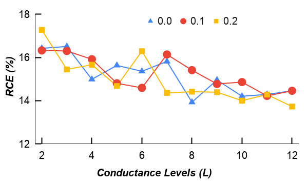
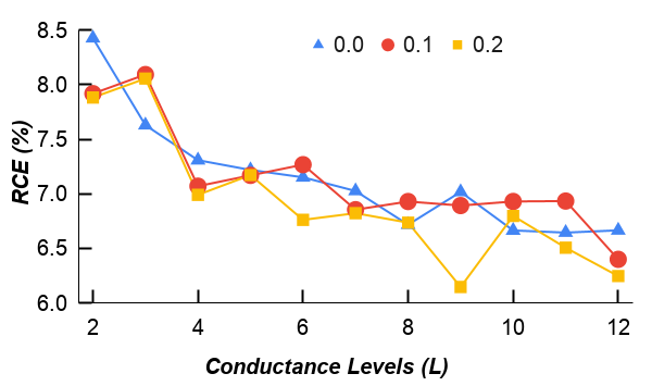
Signal noise
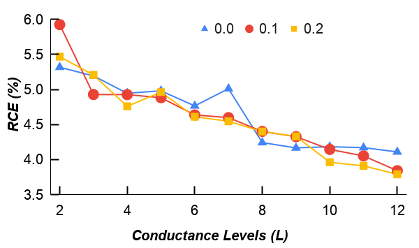
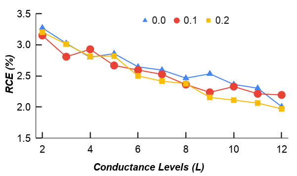
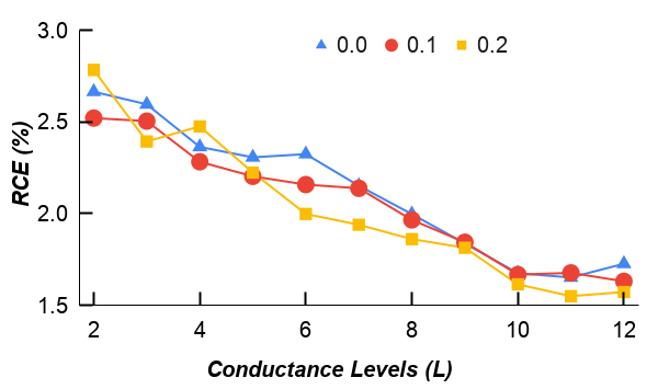
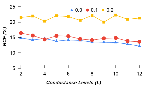
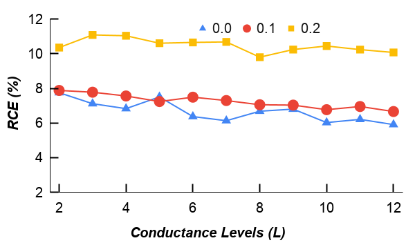
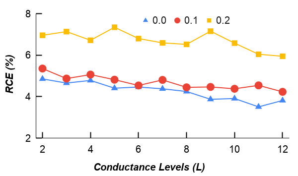
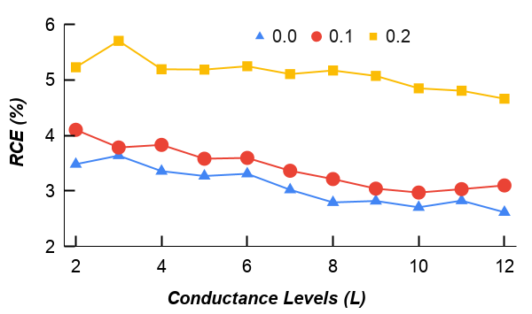
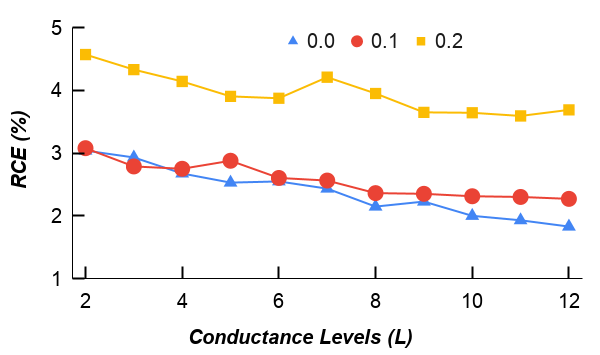
The input signals to the crossbar are prone to noise. This noise can result from sensors or signal integrity issues. To test the impact of signal noise on the superresolution crossbar, we apply additive Gaussian noise with variances, as shown in Fig. 12. The RCE values indicate that the superresolution nodes do not impact the relative accuracy of the current outputs relative to the node with ideal weights.
Effects of wire resistance, read instabilities and variability
To analyse the impact of the crossbar variability, we perform boundary analysis considering the combined effect of wire-resistance, , changes in the crossbar. At each node, the maximum variation is assumed to be 2.5 0.25 for wire resistance, boundary resistances change as and . Table VI shows that when there is wire resistance and changes in boundary resistances, the impact is more evident in a single memristor node and less prominent in super-resolution nodes. Here, N and Y indicate the cases without and with wire resistance, respectively. In both cases, the boundary resistances changes by a maximum 20% standard deviation from the mean and . Read instability [58, 59] can also occur in a crossbar, with the current readouts varying from their mean value. Inclusion of a high read instability, of 10%, on the crossbar readout currents, are shown in the column labelled R in Table VI. Even in this case, the use of multiple memristors per node show far more robustness than single memristor per node crossbar.
| 1-M node | 2-M node | 3-M node | 4-M node | 5-M node | 6-M node | |||||||||||||
|---|---|---|---|---|---|---|---|---|---|---|---|---|---|---|---|---|---|---|
| N | Y | R | N | Y | R | N | Y | R | N | Y | R | N | Y | R | N | Y | R | |
| 2 | 14.7 | 15.5 | 15.7 | 7.8 | 7.8 | 8 | 5.3 | 5.3 | 5.3 | 3.7 | 3.7 | 3.9 | 2.9 | 3 | 3.4 | 2.6 | 2.6 | 2.7 |
| 3 | 7.9 | 8.2 | 10 | 3.8 | 3.8 | 4.7 | 2.5 | 2.4 | 3 | 1.8 | 1.9 | 2.5 | 1.5 | 1.4 | 1.9 | 1.2 | 1.3 | 1.6 |
| 4 | 5.3 | 5.3 | 8.1 | 2.5 | 2.5 | 4 | 1.7 | 1.7 | 2.8 | 1.2 | 1.2 | 2 | 1 | 1 | 1.5 | 0.9 | 0.9 | 1.4 |
| 5 | 3.6 | 3.8 | 7.2 | 1.8 | 1.8 | 3.5 | 1.3 | 1.2 | 2.6 | 0.9 | 1 | 1.7 | 0.8 | 0.7 | 1.4 | 0.6 | 0.6 | 1.1 |
| 6 | 2.9 | 2.9 | 6.8 | 1.4 | 1.5 | 3.4 | 1 | 1 | 2.2 | 0.8 | 0.7 | 1.6 | 0.6 | 0.6 | 1.4 | 0.5 | 0.5 | 1.1 |
| 7 | 2.5 | 2.5 | 6.8 | 1.3 | 1.3 | 3.5 | 0.8 | 0.8 | 2.2 | 0.6 | 0.6 | 1.7 | 0.5 | 0.5 | 1.3 | 0.4 | 0.4 | 1.1 |
| 8 | 2.0 | 2.2 | 6.6 | 1 | 1.1 | 3.5 | 0.8 | 0.7 | 2.2 | 0.5 | 0.5 | 1.7 | 0.4 | 0.4 | 1.4 | 0.3 | 0.4 | 1.1 |
| 9 | 2 .0 | 2.0 | 6.8 | 0.9 | 0.9 | 3.3 | 0.6 | 0.6 | 2.1 | 0.5 | 0.4 | 1.7 | 0.4 | 0.4 | 1.2 | 0.3 | 0.3 | 1 |
| 10 | 1.7 | 1.8 | 6.4 | 0.8 | 0.8 | 3.4 | 0.6 | 0.5 | 2.1 | 0.4 | 0.4 | 1.7 | 0.3 | 0.3 | 1.2 | 0.3 | 0.3 | 1.1 |
| 11 | 1.5 | 1.6 | 6.5 | 0.7 | 0.7 | 3.2 | 0.5 | 0.5 | 2.2 | 0.4 | 0.4 | 1.6 | 0.3 | 0.3 | 1.3 | 0.2 | 0.2 | 1 |
| 12 | 1.3 | 1.4 | 6.4 | 0.7 | 0.7 | 3.2 | 0.5 | 0.4 | 2 | 0.3 | 0.3 | 1.6 | 0.3 | 0.3 | 1.3 | 0.2 | 0.2 | 1.1 |
Application in CNN
To perform the analysis and tests on the crossbar for an analog neural network accelerator application, we select the convolutional neural network and its analog hardware implementation outlined in [55]. The architecture consists of two convolutional and two dense layers, with the circuits for implementing the dropout444Dropout is a technique to regularise neural network by dropping OFF neuronal nodes during the training, which avoids complex co-adaptations and over-fitting on training data. and programming of memristor levels. The circuit design and parameter extraction for CNN circuit blocks in [55] was done in SPICE, while architecture level simulations for calculating performance accuracy with and without variability were performed with customised Python programs.
| 1-M node | 2-M node | 3-M node | 4-M node | 5-M node | 6-M node | 7-M node | 8-M node | ||||||||
| ACC (%) | ACC (%) | ACC (%) | ACC (%) | ACC (%) | ACC (%) | ACC (%) | ACC (%) | ||||||||
| 2 | 82.43 | 3 | 84.10 | 4 | 84.78 | 5 | 85.19 | 6 | 86.66 | 7 | 89.07 | 8 | 90.07 | 9 | 90.41 |
| 3 | 84.10 | 6 | 86.66 | 10 | 90.91 | 15 | 91.14 | 21 | 91.20 | 28 | 91.18 | 36 | 91.26 | 45 | 91.21 |
| 4 | 84.78 | 10 | 90.91 | 20 | 91.19 | 35 | 91.24 | 56 | 91.28 | 84 | 91.22 | 120 | 91.25 | 165 | 91.28 |
| 5 | 85.19 | 15 | 91.14 | 35 | 91.24 | 70 | 91.22 | 126 | 91.26 | 210 | 91.25 | 330 | 91.26 | 495 | 91.26 |
| 6 | 86.66 | 21 | 91.20 | 56 | 91.28 | 126 | 91.26 | 252 | 91.25 | 462 | 91.25 | 792 | 91.26 | 1287 | 91.26 |
| 7 | 89.07 | 28 | 91.18 | 84 | 91.22 | 210 | 91.25 | 462 | 91.25 | 924 | 91.26 | 1716 | 91.26 | 3003 | 91.26 |
| 8 | 90.07 | 36 | 91.26 | 120 | 91.25 | 330 | 91.26 | 792 | 91.26 | 1716 | 91.26 | 3432 | 91.26 | 6435 | 91.26 |
| 9 | 90.41 | 45 | 91.21 | 165 | 91.28 | 495 | 91.26 | 1287 | 91.26 | 3003 | 91.26 | 6435 | 91.26 | 12870 | 91.26 |
| 10 | 90.91 | 55 | 91.22 | 220 | 91.27 | 715 | 91.26 | 2002 | 91.26 | 5005 | 91.26 | 11440 | 91.26 | 24310 | 91.26 |
| 11 | 90.89 | 66 | 91.22 | 286 | 91.27 | 1001 | 91.25 | 3003 | 91.26 | 8008 | 91.26 | 19448 | 91.26 | 43758 | 91.26 |
| 12 | 91.02 | 78 | 91.23 | 364 | 91.27 | 1365 | 91.26 | 4368 | 91.26 | 12376 | 91.26 | 31824 | 91.26 | 75582 | 91.26 |
Table VII shows the recognition accuracy of implementing the CNN accelerator with the proposed memristor crossbar nodes. The CIFAR-10 dataset has ten classes, with each class having 6000 images. The CNN used for testing includes two convolution layers, with average pooling 555Average pooling means calculating the average of each patch of feature maps obtained from the convolution layer, which goes as input to the subsequent layers. and dropout ratio of 0.5, and two dense layers. The first layer uses the ReLu activation function, while the last layer is the softmax function. It can be seen that at the minimum, using two 8-level memristors or seven 3-level memristors gives accuracy that matches with ideal case results of memristor having infinite states, i.e., 91.26%. For reliability of operations, it is more appropriate to use crossbar nodes with more memristors and conductive states. Even if some of the states disappear due to aging, the impact on overall recognition accuracy will be lower. Any conductance level of the memristor can be imagined as having a mean conductance value with a standard variance. If the variance is large, the conductance values can overlap and introduce larger errors. For reducing this impact, it is recommended to allow larger separations between the conductance levels, using more memristors per node with fewer conductance levels. This increases robustness to conductance variations as can be observed in the example of Table VIII, for an 8-M node with or .
| 1-M node | 2-M node | 3-M node | 4-M node | 5-M node | 6-M node | 7-M node | 8-M node | ||||||||
| ACC (%) | ACC (%) | ACC (%) | ACC (%) | ACC (%) | ACC (%) | ACC (%) | ACC (%) | ||||||||
| 2 | 82.5 | 3 | 84.14 | 4 | 84.69 | 5 | 85.37 | 6 | 85.99 | 7 | 88.2 | 8 | 90.13 | 9 | 90.22 |
| 3 | 83.94 | 6 | 86.62 | 10 | 90.63 | 15 | 90.83 | 21 | 90.92 | 28 | 90.97 | 36 | 90.96 | 45 | 91.02 |
| 4 | 84.83 | 10 | 90.55 | 20 | 91 | 35 | 90.94 | 56 | 90.99 | 84 | 90.81 | 120 | 91.02 | 165 | 90.91 |
| 5 | 85.29 | 15 | 90.87 | 35 | 91.01 | 70 | 91 | 126 | 90.96 | 210 | 90.93 | 330 | 91.03 | 495 | 90.99 |
| 6 | 87.3 | 21 | 90.98 | 56 | 90.99 | 126 | 91.01 | 252 | 90.8 | 462 | 91 | 792 | 90.97 | 1287 | 91.06 |
| 7 | 89.11 | 28 | 90.83 | 84 | 90.98 | 210 | 90.9 | 462 | 91.01 | 924 | 91.05 | 1716 | 90.95 | 3003 | 90.91 |
| 8 | 90.16 | 36 | 91.01 | 120 | 90.93 | 330 | 91.02 | 792 | 90.92 | 1716 | 90.87 | 3432 | 90.98 | 6435 | 90.9 |
| 9 | 90.13 | 45 | 90.96 | 165 | 90.92 | 495 | 90.99 | 1287 | 91.01 | 3003 | 90.95 | 6435 | 91.04 | 12870 | 90.8 |
| 10 | 90.64 | 55 | 91 | 220 | 91 | 715 | 90.95 | 2002 | 90.98 | 5005 | 90.92 | 11440 | 91.01 | 24310 | 90.89 |
| 11 | 90.81 | 66 | 91.02 | 286 | 90.83 | 1001 | 90.95 | 3003 | 91 | 8008 | 90.92 | 19448 | 91.05 | 43758 | 90.99 |
| 12 | 90.7 | 78 | 90.94 | 364 | 90.95 | 1365 | 90.9 | 4368 | 90.89 | 12376 | 90.9 | 31824 | 90.98 | 75582 | 91 |
Table VIII shows the recognition accuracy of the CNN accelerator with the proposed memristor crossbar nodes considering a 10% variability in the conductance levels. The variation of conductance is added such that it is random, and at a level follows a Gaussian distribution with maximum standard deviation set at 10% of the mean value. The tests are repeated 30 times, and the average accuracy is reported. It can be observed from Table VIII that the conductance variability reduces the overall accuracy. An increase in the number of memristors shows higher robustness. Here, the CNN is trained and assumed to have obtained optimal weights. These weights are translated to the conductance values of the memristor superresolution nodes. However, the variability of the conductance values moves the weights further away from optimal values. In addition, the changes in conductance can also move the combination of weights back closer to optimal values increasing the accuracy. For example, when (=2, =1) and (=3, =2), the recognition accuracy is slightly higher under variations by 0.07% and 0.04%.
The over fitting in neural networks can be reduced by applying dropout based regularization during training stages. Further, as the neural network size grows, the energy consumption increases in both test and training stages. To address this, dropouts can be applied in both test and training stages, as shown in [60]. The superresolution nodes can use the same control circuits typically required to program a regular crossbar. In addition, by connecting the row-wise inputs together, superresolution nodes can be created without physically changing the regular crossbar design. This makes the approach universal to a wide range of analog neural network implementations, where the performance of large arrays gets affected by the variability of the conductance levels.
The ability of the proposed approach to transforming any multi-level crossbar arrays to analog crossbar arrays offers improvement in precision and accuracy of the crossbar for analog computing. Any reduction in current errors implies higher accuracy of analog neural computations. Further, the superresolution crossbar nodes also provide increased fault tolerance and reliability. Even if any of the memristors fail or remain stuck at fault, the remaining memristors can still offer a high number of conductive states without compromising the analog neural network’s overall performance.
Optimising superresolution crossbar size
Figure 3 shows an example of a node within a crossbar. Figure 13 shows an extension by combining a different number of rows to create superresolution nodes with different values of . This approach can help to optimise the number of memristors required per crossbar for a given application. For example, if nodes are used to create superresolution crossbar nodes, then a total of 48 memristors are required, while the combination of and nodes, as shown in Fig. 13 requires a total of 40 memristors, resulting in lesser usage of crossbar area. To determine the value of for the superresolution node, for a fixed value, the mapping of with and can be applied. Suppose each memristor has , and we want a conductance resolution of 0.1 (i.e., minimum 10 levels per node) and 0.01 (i.e., minimum 100 levels per node) in the crossbar. Then looking at Table III we can determine the value of for 0.1 as 2 (with ), and for 0.01 as 7 (with ). Such optimisation of crossbar will be useful for applications where parts of the input signal vector within an input pattern such as attention or region of interest in images require higher precision of weights in neural network layers than others. Various applications that can be found for this approach is left as an open problem.
V Conclusion
In this paper, a compelling yet straightforward approach to improve the performance and use of a memristive crossbar for analog neural network implementations are presented. The system shows how a conventional crossbar with memristor nodes with limited conductance resolution can be transformed into a high-resolution conductive node. The resolution mapping is obtained by input row mergers resulting in -simplicial conductance sequences, with a non-linear growth in conductance with an increase in memristors per crossbar nodes. The increase in memristors per node, though it increases the area, offers higher computation accuracy and a more straightforward mapping of weight values.
The reduced relative current errors with an increase in memristors per crossbar nodes show improvement in precision and accuracy of the crossbar MAC calculations. This will, in particular, be useful in neural networks with many neurons layers, where even minor variations in the weights will have a more significant impact on inference accuracy. The current errors are not easy to compensate for during the inference stages and require additional fine-tuning. The need for complex fine-tuning circuits during inference stages can be reduced using the proposed super-resolution approach.
Acknowledgements
A. James’s research is supported by industry research grant Ind/001/2020. L. Chua’s research is supported by Grant FA9550-18-1-0016.
References
- [1] H. Zhang, D. Chen, and S.-B. Ko, “New Flexible Multiple-Precision Multiply-Accumulate Unit for Deep Neural Network Training and Inference,” IEEE Transactions on Computers, vol. 69, no. 1, pp. 26–38, jan 2020. [Online]. Available: https://doi.org/10.1109%2Ftc.2019.2936192
- [2] V. Camus, C. Enz, and M. Verhelst, “Survey of Precision-Scalable Multiply-Accumulate Units for Neural-Network Processing,” in 2019 IEEE International Conference on Artificial Intelligence Circuits and Systems (AICAS). IEEE, mar 2019. [Online]. Available: https://doi.org/10.1109%2Faicas.2019.8771610
- [3] J. Kang and T. Kim, “PV-MAC: Multiply-and-accumulate unit structure exploiting precision variability in on-device convolutional neural networks,” Integration, vol. 71, pp. 76–85, mar 2020. [Online]. Available: https://doi.org/10.1016%2Fj.vlsi.2019.11.003
- [4] H. Tann, S. Hashemi, and S. Reda, “Lightweight Deep Neural Network Accelerators Using Approximate SW/HW Techniques,” in Approximate Circuits. Springer International Publishing, dec 2018, pp. 289–305. [Online]. Available: https://doi.org/10.1007%2F978-3-319-99322-5_14
- [5] K. Siu, D. M. Stuart, M. Mahmoud, and A. Moshovos, “Memory Requirements for Convolutional Neural Network Hardware Accelerators,” in 2018 IEEE International Symposium on Workload Characterization (IISWC). IEEE, sep 2018. [Online]. Available: https://doi.org/10.1109%2Fiiswc.2018.8573527
- [6] K. Seto, H. Nejatollahi, J. An, S. Kang, and N. Dutt, “Small Memory Footprint Neural Network Accelerators,” in 20th International Symposium on Quality Electronic Design (ISQED). IEEE, mar 2019. [Online]. Available: https://doi.org/10.1109%2Fisqed.2019.8697641
- [7] H.-J. Yoo, “1.2 Intelligence on Silicon: From Deep-Neural-Network Accelerators to Brain Mimicking AI-SoCs,” in 2019 IEEE International Solid- State Circuits Conference - (ISSCC). IEEE, feb 2019. [Online]. Available: https://doi.org/10.1109%2Fisscc.2019.8662469
- [8] W. Wen, Y. Zhang, and J. Yang, “ReNEW: Enhancing Lifetime for ReRAM Crossbar Based Neural Network Accelerators,” in 2019 IEEE 37th International Conference on Computer Design (ICCD). IEEE, nov 2019. [Online]. Available: https://doi.org/10.1109%2Ficcd46524.2019.00074
- [9] S. Yin, Z. Jiang, J.-S. Seo, and M. Seok, “XNOR-SRAM: In-Memory Computing SRAM Macro for Binary/Ternary Deep Neural Networks,” IEEE Journal of Solid-State Circuits, pp. 1–11, 2020. [Online]. Available: https://doi.org/10.1109%2Fjssc.2019.2963616
- [10] Z. Jiang, S. Yin, J. sun Seo, and M. Seok, “C3SRAM: An In-Memory-Computing SRAM Macro Based on Robust Capacitive Coupling Computing Mechanism,” IEEE Journal of Solid-State Circuits, pp. 1–1, 2020. [Online]. Available: https://doi.org/10.1109%2Fjssc.2020.2992886
- [11] H. Choi, Y. Lee, J.-J. Kim, and S. Yoo, “A Novel In-DRAM Accelerator Architecture for Binary Neural Network,” in 2020 IEEE Symposium in Low-Power and High-Speed Chips (COOL CHIPS). IEEE, apr 2020. [Online]. Available: https://doi.org/10.1109%2Fcoolchips49199.2020.9097642
- [12] Q. Liu, B. Gao, P. Yao, D. Wu, J. Chen, Y. Pang, W. Zhang, Y. Liao, C.-X. Xue, W.-H. Chen, J. Tang, Y. Wang, M.-F. Chang, H. Qian, and H. Wu, “33.2 A Fully Integrated Analog ReRAM Based 78.4TOPS/W Compute-In-Memory Chip with Fully Parallel MAC Computing,” in 2020 IEEE International Solid- State Circuits Conference - (ISSCC). IEEE, feb 2020. [Online]. Available: https://doi.org/10.1109%2Fisscc19947.2020.9062953
- [13] J. A. Starzyk and Basawaraj, “Memristor Crossbar Architecture for Synchronous Neural Networks,” IEEE Transactions on Circuits and Systems I: Regular Papers, vol. 61, no. 8, pp. 2390–2401, aug 2014. [Online]. Available: https://doi.org/10.1109%2Ftcsi.2014.2304653
- [14] C. Yakopcic, M. Z. Alom, and T. M. Taha, “Extremely parallel memristor crossbar architecture for convolutional neural network implementation,” in 2017 International Joint Conference on Neural Networks (IJCNN). IEEE, may 2017. [Online]. Available: https://doi.org/10.1109%2Fijcnn.2017.7966055
- [15] Y. Li, Z. Wang, R. Midya, Q. Xia, and J. J. Yang, “Review of memristor devices in neuromorphic computing: materials sciences and device challenges,” Journal of Physics D: Applied Physics, vol. 51, no. 50, p. 503002, sep 2018. [Online]. Available: https://doi.org/10.1088%2F1361-6463%2Faade3f
- [16] P. Sheridan and W. Lu, “Memristors and Memristive Devices for Neuromorphic Computing,” in Memristor Networks. Springer International Publishing, 2014, pp. 129–149. [Online]. Available: https://doi.org/10.1007%2F978-3-319-02630-5_8
- [17] T. Prodromakis and C. Toumazou, “A review on memristive devices and applications,” in 2010 17th IEEE International Conference on Electronics, Circuits and Systems. IEEE, 2010, pp. 934–937.
- [18] P. Sheridan and W. Lu, “Memristors and memristive devices for neuromorphic computing,” in Handbook of Memristor Networks. Springer, 2019, pp. 369–389.
- [19] G. Milano, S. Porro, I. Valov, and C. Ricciardi, “Nanowire memristors: Recent developments and perspectives for memristive devices based on metal oxide nanowires (adv. electron. mater. 9/2019),” Advanced Electronic Materials, vol. 5, no. 9, p. 1970044, 2019.
- [20] J. Zhu, T. Zhang, Y. Yang, and R. Huang, “A comprehensive review on emerging artificial neuromorphic devices,” Applied Physics Reviews, vol. 7, no. 1, p. 011312, 2020.
- [21] L. Ni, Z. Liu, H. Yu, and R. V. Joshi, “An Energy-Efficient Digital ReRAM-Crossbar-Based CNN With Bitwise Parallelism,” IEEE Journal on Exploratory Solid-State Computational Devices and Circuits, vol. 3, pp. 37–46, dec 2017. [Online]. Available: https://doi.org/10.1109%2Fjxcdc.2017.2697910
- [22] A. Sebastian, M. L. Gallo, R. Khaddam-Aljameh, and E. Eleftheriou, “Memory devices and applications for in-memory computing,” Nature Nanotechnology, mar 2020. [Online]. Available: https://doi.org/10.1038%2Fs41565-020-0655-z
- [23] E. Gale, “Non-ideal memristors for a non-ideal world,” physica status solidi (a), vol. 212, no. 2, pp. 229–238, 2015.
- [24] Y. Jeong, M. A. Zidan, and W. D. Lu, “Parasitic effect analysis in memristor-array-based neuromorphic systems,” IEEE Transactions on Nanotechnology, vol. 17, no. 1, pp. 184–193, 2017.
- [25] O. Krestinskaya, A. Irmanova, and A. P. James, “Memristive non-idealities: Is there any practical implications for designing neural network chips?” in 2019 IEEE International Symposium on Circuits and Systems (ISCAS). IEEE, 2019, pp. 1–5.
- [26] I. Vourkas, D. Stathis, G. C. Sirakoulis, and S. Hamdioui, “Alternative architectures toward reliable memristive crossbar memories,” IEEE Transactions on Very Large Scale Integration (VLSI) Systems, vol. 24, no. 1, pp. 206–217, 2015.
- [27] L. Chua, G. C. Sirakoulis, and A. Adamatzky, Handbook of Memristor Networks. Springer Nature, 2019.
- [28] S. Zhang, G. L. Zhang, B. Li, H. H. Li, and U. Schlichtmann, “Aging-aware Lifetime Enhancement for Memristor-based Neuromorphic Computing,” in 2019 Design Automation & Test in Europe Conference & Exhibition (DATE). IEEE, mar 2019. [Online]. Available: https://doi.org/10.23919%2Fdate.2019.8714954
- [29] J. Bill and R. Legenstein, “A compound memristive synapse model for statistical learning through stdp in spiking neural networks,” Frontiers in neuroscience, vol. 8, p. 412, 2014.
- [30] I. Boybat, M. Le Gallo, S. Nandakumar, T. Moraitis, T. Parnell, T. Tuma, B. Rajendran, Y. Leblebici, A. Sebastian, and E. Eleftheriou, “Neuromorphic computing with multi-memristive synapses,” Nature communications, vol. 9, no. 1, pp. 1–12, 2018.
- [31] I. Boybat, C. Giovinazzo, E. Shahrabi, I. Krawczuk, I. Giannopoulos, C. Piveteau, M. Le Gallo, C. Ricciardi, A. Sebastian, E. Eleftheriou et al., “Multi-reram synapses for artificial neural network training,” in 2019 IEEE International Symposium on Circuits and Systems (ISCAS). IEEE, 2019, pp. 1–5.
- [32] E. Miranda and J. Suñé, “Memristors for Neuromorphic Circuits and Artificial Intelligence Applications.” Materials (Basel), vol. 13, Feb 2020.
- [33] M. Hu, C. Graves, C. Li, Y. Li, N. Ge, E. Montgomery, N. Davila, H. Jiang, R. Williams, J. Yang, Q. Xia, and J. Strachan, “Memristor-Based Analog Computation and Neural Network Classification with a Dot Product Engine.” Adv Mater, vol. 30, Mar 2018.
- [34] S. Kim, H. Kim, S. Hwang, M. Kim, Y. Chang, and B. Park, “Analog Synaptic Behavior of a Silicon Nitride Memristor.” ACS Appl Mater Interfaces, vol. 9, pp. 40 420–40 427, Nov 2017.
- [35] P. Sheridan, F. Cai, C. Du, W. Ma, Z. Zhang, and W. Lu, “Sparse coding with memristor networks.” Nat Nanotechnol, vol. 12, pp. 784–789, Aug 2017.
- [36] T. S. Ngoc, P. K. Van, W. Yang, A. Jo, M. Lee, H. Mo, and K. Min, “Time-Shared Twin Memristor Crossbar Reducing the Number of Arrays by Half for Pattern Recognition.” Nanoscale Res Lett, vol. 12, p. 205, Dec 2017.
- [37] M. Azghadi, B. Linares-Barranco, D. Abbott, and P. Leong, “A Hybrid CMOS-Memristor Neuromorphic Synapse.” IEEE Trans Biomed Circuits Syst, vol. 11, pp. 434–445, Apr 2017.
- [38] K. Kim, J. Zhang, C. Graves, J. Yang, B. Choi, C. Hwang, Z. Li, and R. Williams, “Low-Power, Self-Rectifying, and Forming-Free Memristor with an Asymmetric Programing Voltage for a High-Density Crossbar Application.” Nano Lett, vol. 16, pp. 6724–6732, Nov 2016.
- [39] M. Zidan, H. Omran, R. Naous, A. Sultan, H. Fahmy, W. Lu, and K. Salama, “Single-Readout High-Density Memristor Crossbar.” Sci Rep, vol. 6, p. 18863, Jan 2016.
- [40] S. Truong, S. Shin, S. Byeon, J. Song, H. Mo, and K. Min, “Comparative Study on Statistical-Variation Tolerance Between Complementary Crossbar and Twin Crossbar of Binary Nano-scale Memristors for Pattern Recognition.” Nanoscale Res Lett, vol. 10, p. 405, Dec 2015.
- [41] J. Chen, J. Li, Y. Li, and X. Miao, “Multiply accumulate operations in memristor crossbar arrays for analog computing,” Journal of Semiconductors, vol. 42, no. 1, p. 013104, 2021.
- [42] M. Le Gallo, A. Sebastian, R. Mathis, M. Manica, H. Giefers, T. Tuma, C. Bekas, A. Curioni, and E. Eleftheriou, “Mixed-precision in-memory computing,” Nature Electronics, vol. 1, no. 4, pp. 246–253, 2018.
- [43] C. Mohan, J. M. de la Rosa, E. Vianello, L. Perniola, C. Reita, B. Linares-Barranco, and T. Serrano-Gotarredona, “A Current Attenuator for Efficient Memristive Crossbars Read-Out,” in 2019 IEEE International Symposium on Circuits and Systems (ISCAS). IEEE, may 2019. [Online]. Available: https://doi.org/10.1109%2Fiscas.2019.8702604
- [44] Y. Cassuto, S. Kvatinsky, and E. Yaakobi, “Sneak-path constraints in memristor crossbar arrays,” in 2013 IEEE International Symposium on Information Theory. IEEE, jul 2013. [Online]. Available: https://doi.org/10.1109%2Fisit.2013.6620207
- [45] L. Shi, G. Zheng, B. Tian, B. Dkhil, and C. Duan, “Research progress on solutions to the sneak path issue in memristor crossbar arrays,” Nanoscale Advances, vol. 2, no. 5, pp. 1811–1827, 2020. [Online]. Available: https://doi.org/10.1039%2Fd0na00100g
- [46] F. Gül, “Addressing the sneak-path problem in crossbar RRAM devices using memristor-based one Schottky diode-one resistor array,” Results in Physics, vol. 12, pp. 1091–1096, mar 2019. [Online]. Available: https://doi.org/10.1016%2Fj.rinp.2018.12.092
- [47] Y. Cassuto, S. Kvatinsky, and E. Yaakobi, “Information-Theoretic Sneak-Path Mitigation in Memristor Crossbar Arrays,” IEEE Transactions on Information Theory, vol. 62, no. 9, pp. 4801–4813, sep 2016. [Online]. Available: https://doi.org/10.1109%2Ftit.2016.2594798
- [48] R. Naous, M. A. Zidan, A. Sultan-Salem, and K. N. Salama, “Memristor based crossbar memory array sneak path estimation,” in 2014 14th International Workshop on Cellular Nanoscale Networks and their Applications (CNNA). IEEE, jul 2014. [Online]. Available: https://doi.org/10.1109%2Fcnna.2014.6888656
- [49] S. Kannan, R. Karri, and O. Sinanoglu, “Sneak path testing and fault modeling for multilevel memristor-based memories,” in 2013 IEEE 31st International Conference on Computer Design (ICCD). IEEE, oct 2013. [Online]. Available: https://doi.org/10.1109%2Ficcd.2013.6657045
- [50] M. Shevgoor, N. Muralimanohar, R. Balasubramonian, and Y. Jeon, “Improving memristor memory with sneak current sharing,” in 2015 33rd IEEE International Conference on Computer Design (ICCD). IEEE, oct 2015. [Online]. Available: https://doi.org/10.1109%2Ficcd.2015.7357164
- [51] D. J. Mountain, M. R. McLean, and C. D. Krieger, “Memristor Crossbar Tiles in a Flexible General Purpose Neural Processor,” IEEE Journal on Emerging and Selected Topics in Circuits and Systems, vol. 8, no. 1, pp. 137–145, mar 2018. [Online]. Available: https://doi.org/10.1109%2Fjetcas.2017.2767024
- [52] D. Mikhailenko, C. Liyanagedera, A. P. James, and K. Roy, “M2CA: Modular Memristive Crossbar Arrays,” in 2018 IEEE International Symposium on Circuits and Systems (ISCAS). IEEE, 2018. [Online]. Available: https://doi.org/10.1109%2Fiscas.2018.8351112
- [53] D. J. Mannion, A. Mehonic, W. H. Ng, and A. J. Kenyon, “Memristor-Based Edge Detection for Spike Encoded Pixels,” Frontiers in Neuroscience, vol. 13, jan 2020. [Online]. Available: https://doi.org/10.3389%2Ffnins.2019.01386
- [54] A. Irmanova, A. Maan, A. James, and L. Chua, “Analog self-timed programming circuits for aging memristors,” IEEE Transactions on Circuits and Systems II: Express Briefs, 2020.
- [55] O. Krestinskaya, B. Choubey, and A. James, “Memristive gan in analog,” Scientific Reports, vol. 10, no. 1, pp. 1–14, 2020.
- [56] P. Jain, U. Arslan, M. Sekhar, B. C. Lin, L. Wei, T. Sahu, J. Alzate-vinasco, A. Vangapaty, M. Meterelliyoz, N. Strutt et al., “13.2 a 3.6 mb 10.1 mb/mm 2 embedded non-volatile reram macro in 22nm finfet technology with adaptive forming/set/reset schemes yielding down to 0.5 v with sensing time of 5ns at 0.7 v,” in 2019 IEEE International Solid-State Circuits Conference-(ISSCC). IEEE, 2019, pp. 212–214.
- [57] “The generalized metastable switch memristor model.” [Online]. Available: https://knowm.org/the-generalized-metastable-switch-memristor-model/
- [58] S. Wiefels, C. Bengel, N. Kopperberg, K. Zhang, R. Waser, and S. Menzel, “Hrs instability in oxide-based bipolar resistive switching cells,” IEEE Transactions on Electron Devices, vol. 67, no. 10, pp. 4208–4215, 2020.
- [59] F. M. Puglisi, N. Zagni, L. Larcher, and P. Pavan, “Random telegraph noise in resistive random access memories: Compact modeling and advanced circuit design,” IEEE Transactions on Electron Devices, vol. 65, no. 7, pp. 2964–2972, 2018.
- [60] O. Krestinskaya and A. James, “Analogue neuro-memristive convolutional dropout,” Proc. R. Soc. A, 2020.