High Permittivity Dielectric Field-Plated Vertical (001) -Ga2O3 Schottky Barrier Diode with Surface Breakdown Electric Field of 5.45 MV/cm and BFOM of 1 GW/cm2
Abstract
This paper presents vertical (001) oriented -Ga2O3 field plated (FP) schottky barrier diode (SBD) with a novel extreme permittivity dielectric field oxide. A thin drift layer of 1.7 was used to enable a punch-through (PT) field profile and very low differential specific on- resistance (Ron-sp) of 0.32 m-cm2. The extreme permittivity field plate oxide facilitated the lateral spread of the electric field profile beyond the field plate edge and enabled a breakdown voltage () of 687 V. The edge termination efficiency increases from 13.5 for non-field plated structure to 63 for high permittivity field plate structure. The surface breakdown electric field was extracted to be of 5.45 MV/cm at the center of the anode region using TCAD simulations. The high permittivity field plated SBD demonstrated a record high Baliga’s figure of merit (BFOM) of 1.47 GW/cm2 showing the potential of Ga2O3 power devices for multi-kilovolt class applications.
Index Terms:
Ga2O3, Field Plate, High-k, Schottky diode, Edge Termination, Power Device, HVPEI Introduction
The rise of -Ga2O3 as the next generation power electronic material due to its large bandgap (4.6 eV) and very high Baliga’s figure of merit (3400Si) [1] has enabled researchers to demonstrate multi-kilovolt class devices regardless of its recent inception. The estimated critical electric field of -Ga2O3 (8 MV/cm) is significantly higher than GaN (3.3 MV/cm) and SiC (2.4 MV/cm) holding promise for applications with very high voltage blocking capabilities. Various power devices including SBDs and transistors in both lateral and vertical geometry have been demonstrated with high breakdown voltages [2, 3, 4, 5, 6, 7, 8, 9, 10, 11, 12, 13, 14, 15, 16].
Despite its huge potential, -Ga2O3 poses several challenges regarding the management of electric field at the device corners and edges, causing premature breakdown of devices. The lack of p-type doping, which is widely used in GaN and SiC devices for edge field management also poses a fundamental challenge in device design and complicated hetero-integration is needed for -Ga2O3 [17]. Even with non p-type edge terminations, the average electric field for demonstrated -Ga2O3 devices are far lower than the theoretical material limit. Hence, search of robust and efficient alternative edge termination techniques are necessary to rival the existing ultra-wide bandgap material-based devices.
In this paper, we demonstrate a field plated vertical Schottky barrier diode with an extreme permittivity (BaTiO3/SrTiO3) [18] field plate oxide [19] with punch through design. By achieving a high dielectric constant of 325, we have managed to increase the surface electric field at breakdown to 5.45 MV/cm. A breakdown voltage of 687 V in conjunction with a very low Ron-sp (0.32 m-cm2) has resulted in a record high BFOM of 1.47 GW/cm2. TCAD simulation is also performed to estimate the field distribution and the breakdown location in the fabricated devices.
II Device Fabrication
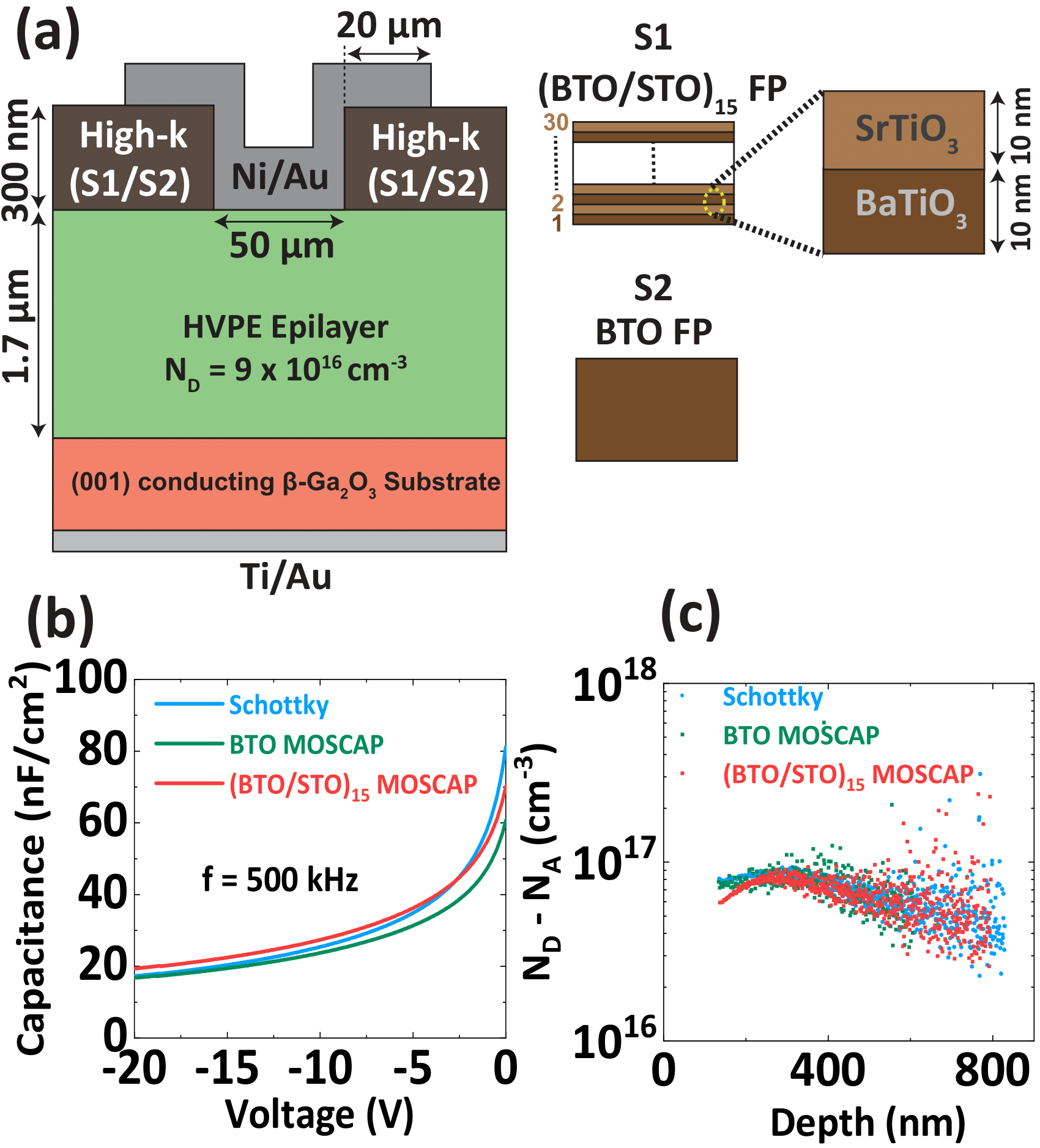
Device fabrication of the field plated SBD as shown in Fig. 1(a) started with the growth of the (001) -Ga2O3 epilayers in a custom-designed subatmospheric vertical HVPE reactor using GaCl and O2 precursors [20]. GaCl is produced in-situ by flowing Cl2 over liquid Ga (7N purity), and is subsequently transported to the wafer surface through a quartz injector. Growth rates are controlled by the GaCl molar flow rates, and for these films the growth rates were 5 per hour. Before the device fabrication, the samples were dipped in HF followed by HCl for 5 minutes. 15 layers of 10 nm thick BaTiO3 and SrTiO3 (BTO/STO)15 (Total 300 nm) were sputter deposited on the samples in oxygen ambient at room temperature. After the dielectric deposition, the samples were annealed at 700 0C in oxygen ambient for 30 minutes to increase the dielectric constant. The sample was then patterned using standard photolithography and the active regions were opened-up using SF6/Ar dry etching. About 50 nm of overetching is performed to ensure the complete removal of the dielectrics which was confirmed using transmission electron microscope imaging (53 nm). Ni/Au (50/100 nm) metal stacks were then deposited on the sample using e-beam evaporation. Finally, Ti/Au (50/100 nm) ohmic contacts were sputter deposited on the back side of the sample. An additional sample with BaTiO3 (BTO) dielectric as field plate oxide was also fabricated for comparison using the process flow described above. Besides the SBDs with (BTO/STO)15 FP and BTO FP, SBDs with no FPs were also fabricated on a reference sample.
III Results And Discussions
To understand effects of the dielectric deposition and the thermal annealing on the carrier concentration, capacitance voltage (CV) measurements were performed as shown in Fig. 1(b) for the schottky diode, BTO MOSCAP, and (BTO/STO)15 MOSCAP. A doping concentration of 8-91016 cm-3 is extracted from the CV plot as shown in Fig. 1(c). Dielectric constants of the deposited (BTO/STO)15 and BTO layer were extracted to be 325 and 142 by depositing the dielectrics on an MOCVD grown (010) -Ga2O3 with a delta doped layer as reported by Xia et al. [10].
The typical current voltage plots in log and linear scale are shown in Fig. 2(a) and 2(b) respectively. The ideality factor (n) is extracted to be 1.04, 1.1 and 1.07 for the non- field plated SBD, BTO FP SBD, (BTO/STO)15 FP SBD respectively. The Ron-sp for the non-field plated, BTO FP, and (BTO/STO)15 SBDs from the linear fit of the IV characteristics are extracted to be 0.33, 0.34, and 0.35 m-cm2 respectively and the lowest differential Ron-sp are 0.32, 0.34, and 0.32 m-cm2 respectively. Nominally similar values of ideality factor and on-resistance measured in all the three samples indicates that the dielectric deposition and the dry etching process of the dielectric did not degrade the drift layer and the metal/semiconductor interface.
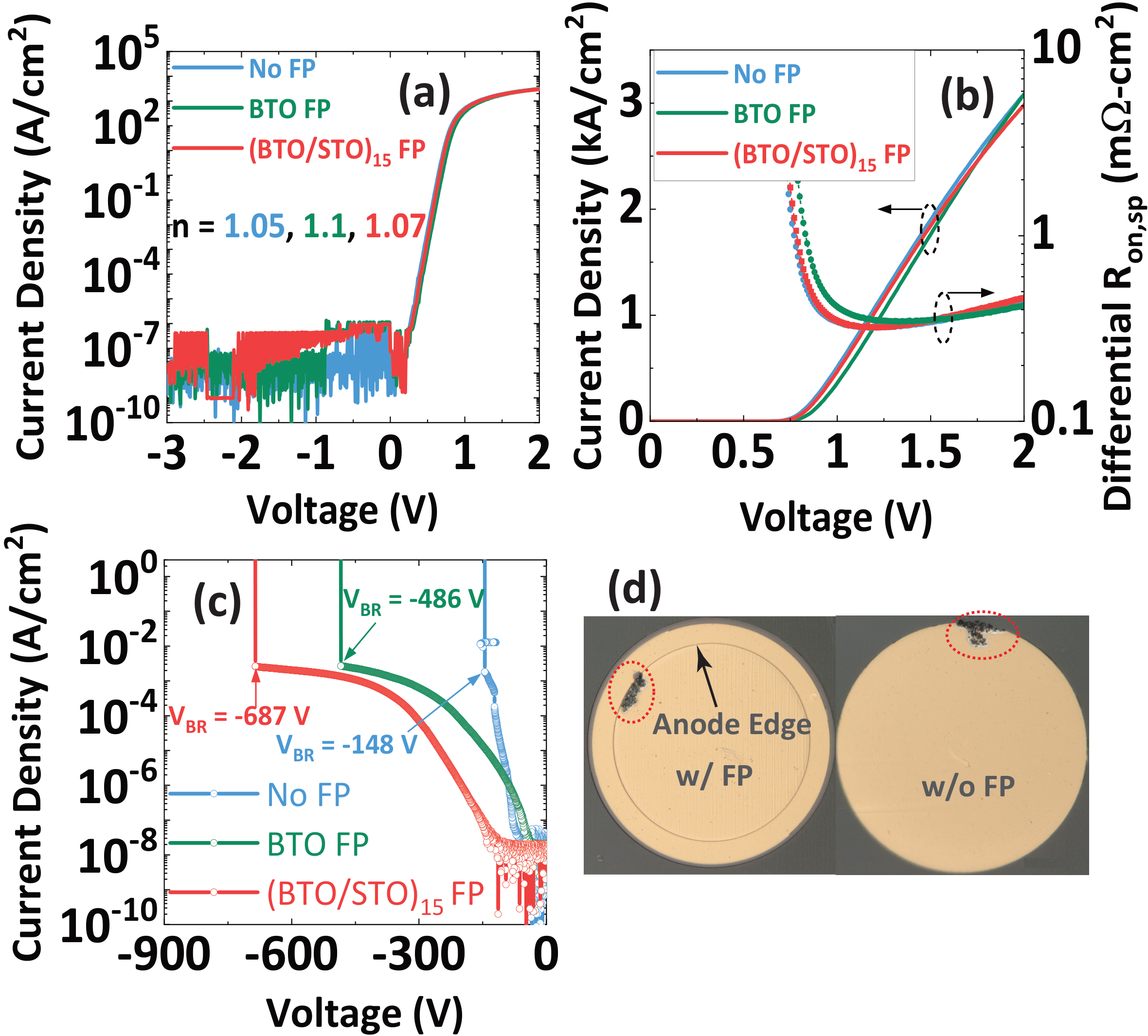
The breakdown characteristics for the SBDs with no FP, BTO FP, and (BTO/STO)15 FP are shown in Fig. 2(c). The destructive breakdown voltages for the three devices are extracted to be 148 V, 486 V and 687 V respectively. The breakdown craters were observed at the anode edges as shown in the the optical microscope image of Fig. 2(d) for the FP and non-FP SBDs indicating the location of the breakdown. The increase in breakdown voltages for the high permittivity dielectric field plate oxide suggests the effectiveness of the edge termination and reduction in field crowding at the device edges due to the high permittivity of the FP dielectric.
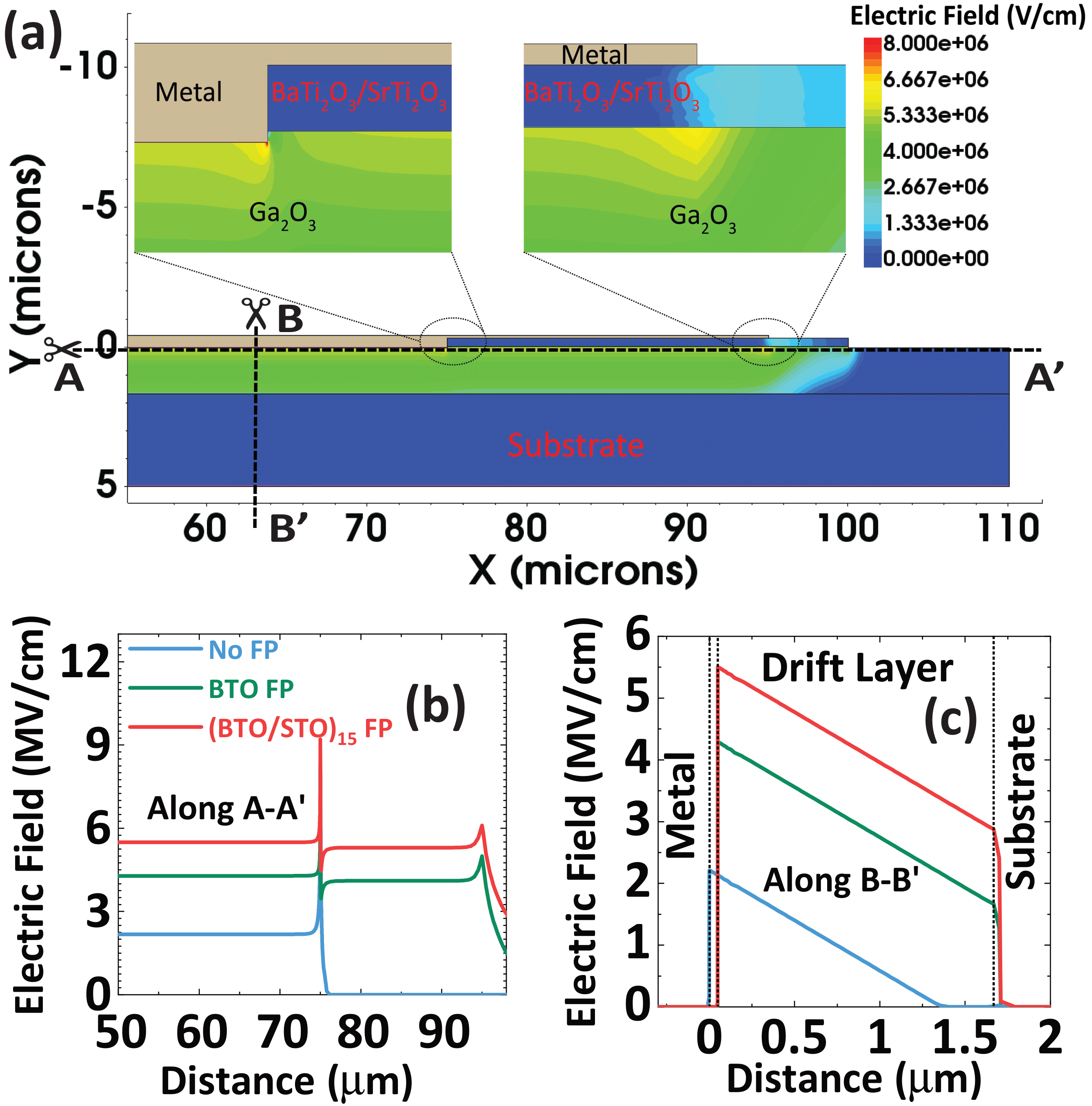
The electric field simulations for the three SBD structures are also performed using Sentaurus TCAD software [21] and results are plotted in Fig. 3(a), (b), and (c). Except for the non-field plated SBD, the other two devices reach punch through condition at breakdown as can be seen from Fig. 3(c). The calculated surface electric field (Esurf) for the non-punch-through and punch-through devices can be calculated as and respectively, where is the electron charge, is the donor concentration, is the relative permittivity, and is the thickness of drift layer. Using the above two expressions, the surface electric fields can be calculated for SBD with no FP as 2.2 MV/cm, with BTO FP as 4.2 MV/cm, with (BTO/STO)15 FP as 5.42 MV/cm. The calculated values for electric field match exactly with the simulation values as can be seen in Fig. 3(b), showing the validity of our simulations. This maximum surface electric field of 5.45 MV/cm for SBD with (BTO/STO)15 FP is the highest value reported to date for all the Schottky barrier diodes. A peak electric field of 8-9 MV/cm was estimated at anode edges suggesting the location of the breakdown, thus, confirming the weak points for each type of device as seen in the microscope images shown in Fig. 2(d) . The edge termination efficiency ([Real /Ideal ] ×100) increases from 44.2 for the BTO FP to 63 for (BTO/STO)15 FP, where Ideal is calculated from the Esurf expressions mentioned above by replacing Esurf with EC (the critical electric field).
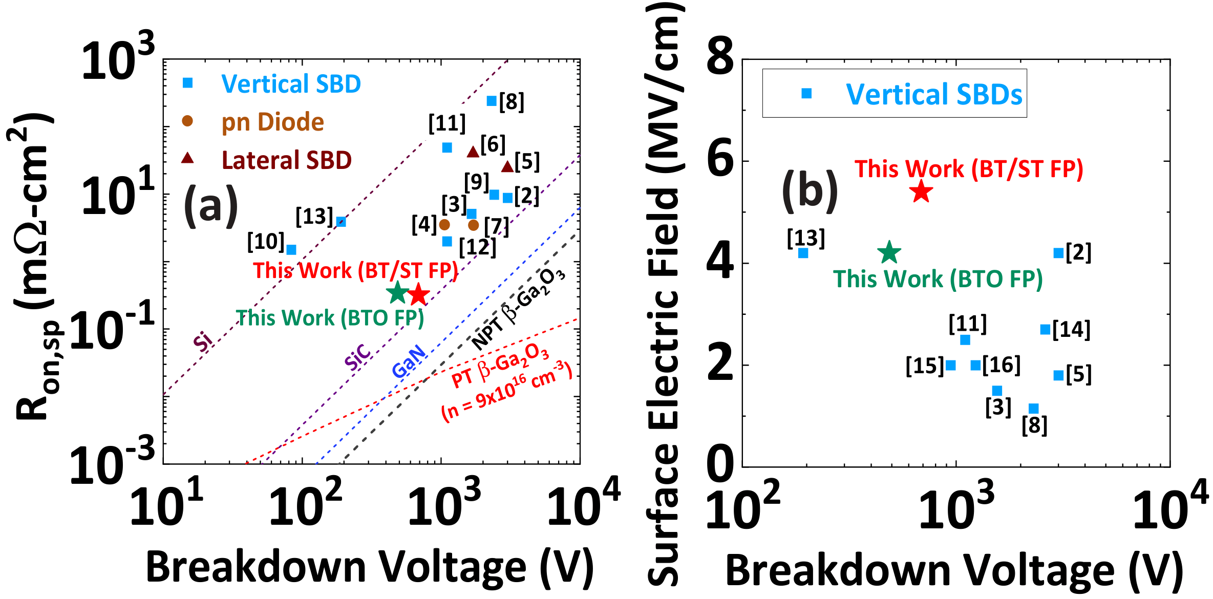
The extremely low Ron-sp of 0.32 m-cm2 (0.35 m-cm2 from linear fit) and the breakdown voltage of 687 V for the (BTO/STO)15 FP SBD results in a record high figure of merit of 1.47 GW/cm2 (1.34 GW/cm2 for the linear fit Ron-sp=0.35 m-cm2). Fig. 4(a) shows the benchmark plots of Ron-sp and breakdown voltage comparing performance of the (BTO/STO)15 FP SBD with the existing literature reports. The performance metrics of our device is significantly better compared to the other reported devices. The surface breakdown electric field of 5.45 MV/cm is the highest electric field reported to date for -Ga2O3 based SBDs as can be seen from Fig. 4(b). The device design of SBD demonstrated here using high permittivity field plate oxide has the potential to achieve the theoretical critical electric field of -Ga2O3 showing promise for next generation power electronics.
IV Conclusion
In summary we have demonstrated a vertical (001) oriented -Ga2O3 SBD with high permittivity dielectric field plate oxide showing extremely low Ron-sp of 0.32 m-cm2 and a high breakdown voltage of 687 V resulting in a BFOM value of 1.47 GW/cm2 surpassing all the reported SBDs. The surface breakdown electric field of 5.45 MV/cm is the highest electric field reported to date for -Ga2O3 SBDs. This demonstration indicates that the use of such high-permittivity dielectric field-plated structure enables high edge field termination efficiency and also enable studying the intrinsic critical field limits of ultra-wide band-gap semiconductors.
References
- [1] S. Pearton, J. Yang, P. H. Cary IV, F. Ren, J. Kim, M. J. Tadjer, and M. A. Mastro, “A review of Ga2O3 materials, processing, and devices,” Applied Physics Reviews, vol. 5, no. 1, p. 011301, 2018.
- [2] W. Li, K. Nomoto, Z. Hu, D. Jena, and H. G. Xing, “Field-Plated Ga2O3 Trench Schottky Barrier Diodes With a BV2/Ron-sp of up to 0.95 GW/cm2,” IEEE Electron Device Letters, vol. 41, no. 1, pp. 107–110, 2019.
- [3] H. Zhou, Q. Yan, J. Zhang, Y. Lv, Z. Liu, Y. Zhang, K. Dang, P. Dong, Z. Feng, Q. Feng et al., “High-Performance Vertical -Ga2O3 Schottky Barrier Diode With Implanted Edge Termination,” IEEE Electron Device Letters, vol. 40, no. 11, pp. 1788–1791, 2019.
- [4] X. Lu, X. Zhou, H. Jiang, K. W. Ng, Z. Chen, Y. Pei, K. M. Lau, and G. Wang, “1-kV Sputtered p-NiO/n-Ga2O3 Heterojunction Diodes With an Ultra-Low Leakage Current Below 1 A/cm2,” IEEE Electron Device Letters, vol. 41, no. 3, pp. 449–452, 2020.
- [5] Z. Hu, H. Zhou, Q. Feng, J. Zhang, C. Zhang, K. Dang, Y. Cai, Z. Feng, Y. Gao, X. Kang et al., “Field-Plated Lateral -Ga2O3 Schottky Barrier Diode With High Reverse Blocking Voltage of More Than 3 kV and High DC Power Figure-of-Merit of 500 MW/cm2,” IEEE Electron Device Letters, vol. 39, no. 10, pp. 1564–1567, 2018.
- [6] Z. Hu, H. Zhou, K. Dang, Y. Cai, Z. Feng, Y. Gao, Q. Feng, J. Zhang, and Y. Hao, “Lateral -Ga2O3 Schottky barrier diode on sapphire substrate with reverse blocking voltage of 1.7 kV,” IEEE Journal of the Electron Devices Society, vol. 6, pp. 815–820, 2018.
- [7] Y. Lv, Y. Wang, X. Fu, S. Dun, Z. Sun, H. Liu, X. Zhou, X. Song, K. Dang, S. Liang, J. Zhang, H. Zhou, Z. Feng, S. Cai, and Y. Hao, “Demonstration of -Ga2O3 Junction Barrier Schottky Diodes with a Baliga’s Figure of Merit of 0.85 GW/cm2 or a 5A/700 V Handling Capabilities,” IEEE Transactions on Power Electronics, vol. 36, no. 6, pp. 6179–6182, 2021.
- [8] J. Yang, F. Ren, M. Tadjer, S. Pearton, and A. Kuramata, “2300V reverse breakdown voltage Ga2O3 Schottky rectifiers,” ECS Journal of Solid State Science and Technology, vol. 7, no. 5, p. Q92, 2018.
- [9] W. Li, Z. Hu, K. Nomoto, R. Jinno, Z. Zhang, T. Q. Tu, K. Sasaki, A. Kuramata, D. Jena, and H. G. Xing, “2.44 kV Ga2O3 vertical trench Schottky barrier diodes with very low reverse leakage current,” in 2018 IEEE International Electron Devices Meeting (IEDM). IEEE, 2018, pp. 8–5.
- [10] Z. Xia, H. Chandrasekar, W. Moore, C. Wang, A. J. Lee, J. McGlone, N. K. Kalarickal, A. Arehart, S. Ringel, F. Yang et al., “Metal/BaTiO3/-Ga2O3 dielectric heterojunction diode with 5.7 MV/cm breakdown field,” Applied Physics Letters, vol. 115, no. 25, p. 252104, 2019.
- [11] Z. Jian, S. Mohanty, and E. Ahmadi, “Temperature-dependent current-voltage characteristics of -Ga2O3 trench Schottky barrier diodes,” Applied Physics Letters, vol. 116, no. 15, p. 152104, 2020.
- [12] N. Allen, M. Xiao, X. Yan, K. Sasaki, M. J. Tadjer, J. Ma, R. Zhang, H. Wang, and Y. Zhang, “Vertical Ga2O3 Schottky Barrier Diodes With Small-Angle Beveled Field Plates: A Baliga’s Figure-of-Merit of 0.6 GW/cm2,” IEEE Electron Device Letters, vol. 40, no. 9, pp. 1399–1402, 2019.
- [13] C. Joishi, S. Rafique, Z. Xia, L. Han, S. Krishnamoorthy, Y. Zhang, S. Lodha, H. Zhao, and S. Rajan, “Low-pressure CVD-grown -Ga2O3 bevel-field-plated Schottky barrier diodes,” Applied Physics Express, vol. 11, no. 3, p. 031101, 2018.
- [14] W. Li, K. Nomoto, Z. Hu, T. Nakamura, D. Jena, and H. Xing, “Single and multi-fin normally-off Ga2O3 vertical transistors with a breakdown voltage over 2.6 kV,” in 2019 IEEE International Electron Devices Meeting (IEDM). IEEE, 2019, pp. 12–4.
- [15] Y. Wang, Y. Lv, S. Long, X. Zhou, X. Song, S. Liang, T. Han, X. Tan, Z. Feng, S. Cai et al., “High-Voltage (01) -Ga2O3 Vertical Schottky Barrier Diode With Thermally-Oxidized Termination,” IEEE Electron Device Letters, vol. 41, no. 1, pp. 131–134, 2019.
- [16] W. Li, Z. Hu, K. Nomoto, Z. Zhang, J.-Y. Hsu, Q. T. Thieu, K. Sasaki, A. Kuramata, D. Jena, and H. G. Xing, “1230 V -Ga2O3 trench Schottky barrier diodes with an ultra-low leakage current of 1 A/cm2,” Applied Physics Letters, vol. 113, no. 20, p. 202101, 2018.
- [17] S. Roy, A. Bhattacharyya, and S. Krishnamoorthy, “Design of a -Ga2O3 Schottky Barrier Diode With p-Type III-Nitride Guard Ring for Enhanced Breakdown,” IEEE Transactions on Electron Devices, vol. 67, no. 11, pp. 4842–4848, 2020.
- [18] L. Kim, D. Jung, J. Kim, Y. S. Kim, and J. Lee, “Strain manipulation in BaTiO3/SrTiO3 artificial lattice toward high dielectric constant and its nonlinearity,” Applied physics letters, vol. 82, no. 13, pp. 2118–2120, 2003.
- [19] H.-S. Lee, N. K. Kalarickal, M. W. Rahman, Z. Xia, W. Moore, C. Wang, and S. Rajan, “High-permittivity dielectric edge termination for vertical high voltage devices,” Journal of Computational Electronics, vol. 19, no. 4, pp. 1538–1545, 2020.
- [20] J. Leach, K. Udwary, J. Rumsey, G. Dodson, H. Splawn, and K. Evans, “Halide vapor phase epitaxial growth of -Ga2O3 and -Ga2O3 films,” APL Materials, vol. 7, no. 2, p. 022504, 2019.
- [21] Sentaurus Device User Manual, (Version N-2017.09, March 2017).