Quantum networks based on color centers in diamond
Abstract
With the ability to transfer and process quantum information, large-scale quantum networks will enable a suite of fundamentally new applications, from quantum communications to distributed sensing, metrology, and computing. This perspective reviews requirements for quantum network nodes and color centers in diamond as suitable node candidates. We give a brief overview of state-of-the-art quantum network experiments employing color centers in diamond, and discuss future research directions, focusing in particular on the control and coherence of qubits that distribute and store entangled states, and on efficient spin-photon interfaces. We discuss a route towards large-scale integrated devices combining color centers in diamond with other photonic materials and give an outlook towards realistic future quantum network protocol implementations and applications.
With the Panama-Pacific International Exposition of 1914 fast approaching, AT&T’s leadership grew increasingly alarmed: it was still impossible to hold a coast-to-coast telephone call, despite the company touting it for years. The essential problem “was a satisfactory telephone repeater,” recalled an AT&T senior manager from conversations with the company’s chief engineer John J. Carty Gertner (2012). Whereas mechanical repeaters adequately boosted voice signals on the metro-scale, they added so much noise that signals quickly became unintelligible over longer distances. A fundamentally new repeater technology was needed. Tasked with this urgent mission, Bell Laboratories developed the “audion” trion vacuum tube, just in time for the 1914 Exposition. Over the ensuing decades, the triode made way to the transistor, copper wires yielded to optical fiber, and binary digits (”bits") became the universal language of information, transcending physical modality. Today, as the authors edit these sentences over a globe-spanning video conference, the world is at the cusp of the next information revolution, as quantum bits (”qubits") have become the universal units fueling a new generation of ‘quantum information technologies’. And once again, an essential challenge is to develop a “satisfactory repeater” – this time, capable of relaying (but not amplifying! Park (1970)) quantum information signals. This article reviews the progress towards one such “quantum repeater” as well as other quantum network technology using color centers in diamond to connect quantum information among spins and photons.
I A brief introduction to quantum networks
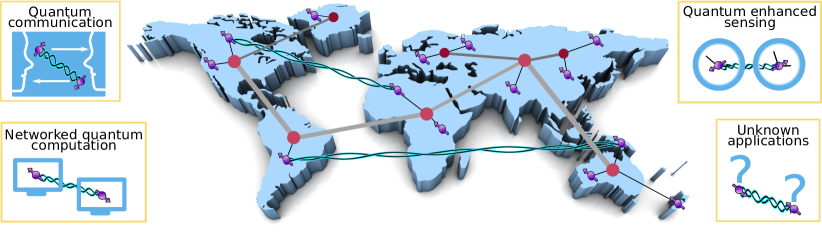
In a future quantum network (see Fig. 1), remote parties are connected by sharing long-lived entangled states Kimble (2008); Wehner, Elkouss, and Hanson (2018). Arguably, the most promising way of linking distant nodes is to employ fiber- or free-space photonic communication channels to establish entanglement. While all photon-based schemes are associated with losses that scale with distance Pirandola et al. (2017), motivating the need for quantum repeaters Briegel et al. (1998), heralding entanglement generation on successful photon transmission events maps these losses into reduced entanglement generation rates without lowering entanglement fidelities Cabrillo et al. (1999); Barrett and Kok (2005); Duan and Kimble (2004).
Optically-mediated remote entanglement of individually controllable qubits has been generated for different materials platforms, including quantum dots Delteil et al. (2016); Stockill et al. (2017), trapped ions Moehring et al. (2007); Hucul et al. (2015); Stephenson et al. (2020), neutral atoms Ritter et al. (2012); Hofmann et al. (2012); Daiss et al. (2021); Langenfeld et al. (2021), and nitrogen-vacancy centers in diamond Bernien et al. (2013); Hensen et al. (2015). Other promising systems, including so-called group-IV defects in diamond Bhaskar et al. (2017); Nguyen et al. (2019a); Bhaskar et al. (2020); Trusheim et al. (2020), defects in SiC Nagy et al. (2019); Bourassa et al. (2020); Lukin, Guidry, and Vučković (2020), and rare-earth ions in solid-state hosts Raha et al. (2020); Kindem et al. (2020); Merkel, Ulanowski, and Reiserer (2020), show great potential for quantum network applications, although remote entanglement has not yet been generated. Another less explored approach is to link distant superconducting quantum processors using coherent conversion of microwave photons to telecom frequencies Chu and Gröblacher (2020); Mirhosseini et al. (2020); Forsch et al. (2020); Hease et al. (2020); Krastanov et al. (2020).
Apart from fundamental tests of physics Hensen et al. (2015), small-scale quantum networks have been used to demonstrate key network protocols such as non-local quantum gates Daiss et al. (2021), entanglement distillation Kalb et al. (2017), and very recently entanglement swapping Pompili et al. (2021). These networks are currently limited to a few nodes Pompili et al. (2021), distances of up to one kilometer Hensen et al. (2015), and entanglement generation rates in the Hz to kHz regime Delteil et al. (2016); Stockill et al. (2017); Moehring et al. (2007); Hucul et al. (2015); Stephenson et al. (2020); Ritter et al. (2012); Hofmann et al. (2012); Bernien et al. (2013); Hensen et al. (2015). A major challenge for the coming decade is to transition from the current proof-of-principle experiments to large-scale quantum networks for use in fields such as distributed quantum computation Nickerson, Fitzsimons, and Benjamin (2014); Choi et al. (2019), quantum enhanced sensing Gottesman, Jennewein, and Croke (2012); Kómár et al. (2014), and quantum secure communication Ekert and Renner (2014).
In this perspective article, we focus on color centers in diamond as potential building blocks for large-scale quantum networks. We identify their strengths and challenges, current research trends, and open questions, with a focus on qubit control, coherence, and efficient spin-photon interfaces. We lay out a path towards large-scale, integrated devices, and discuss possible protocols and functionalities such devices could enable.
This article is organized as follows: Sec. II introduces the requirements for the nodes of a quantum network and gives a high-level overview of why color centers in diamond are promising candidates to meet these demands. We then give a brief overview of state-of-the-art quantum network experiments employing color centers in diamond in Sec. III, to give the reader a sense of the current research status. In Sec. IV, we introduce the physics behind color centers in diamond, to understand their strengths and challenges for quantum network applications in the remainder of this article. Sec. V discusses open questions regarding the coherence and control of nuclear spin memory qubits surrounding color centers in diamond that can be used as additional quantum resources. In Sec. VI, we outline the need and strategies for an enhancement of the spin-photon interface of diamond color centers and discuss promising future research in this direction. Sec. VII outlines a path towards large-scale, integrated diamond devices that may enable future quantum network experiments with high rates. Finally, Sec. VIII concludes by illuminating possible applications for future quantum networks.
II Requirements for a quantum network node
To make a material platform suitable for a node in a quantum network in which entanglement is mediated by photons, it has to fulfill three main requirements Wehner, Elkouss, and Hanson (2018). First, the capability to interface at least one qubit efficiently with optical photons (at telecommunication wavelengths for fiber-based systems), to establish remote entanglement at high rates. Second, the ability to store quantum states during entanglement generation; in particular, this requires qubit coherence times under full network activity to be longer than the time it takes to generate entanglement between nodes. Third, the capability to store several entangled states per node with a capability for high-fidelity operations between them, to enable multi-qubit protocols such as error correction.
Color centers in diamond satisfy most of these requirements, and have enabled some of the most advanced experimental demonstrations of quantum network protocols to date. We here give a concise, high level overview of the achieved and projected key capabilities of color centers in diamond [see Fig. 2(a)], motivating a detailed treatment (and also including the relevant literature) in the remains of this article:
-
1.
The color center contains an individually controllable, optically active spin (communication qubit), with access to several long-lived nuclear spins (memory qubits) in its surrounding. These memory qubits can be manipulated with high fidelity to free up the communication qubit and enable multi-qubit protocols. They have a long coherence time enabling robust state storage during subsequent network activity.
-
2.
The internal level structure is suited to generate remote entanglement. In particular, color centers feature spin-state-selective optical transitions that can entangle the color center’s spin state with a photonic state, e.g. in the number / polarization / time basis (see Fig. 2(b).)
-
3.
Optical emission of color centers is bright and can be collected with high efficiency, enabling high entanglement generation rates. This emission is in the visible to near-IR spectrum, and thus at wavelengths that are associated with higher fiber transmission losses than for photons in the telecom band. However, it is possible to efficiently convert this emission to the telecom band while maintaining quantum correlations.
-
4.
Diamond is a solid-state material, potentially enabling nanophotonic device fabrication at a large scale. Such devices can also be integrated with photonic circuits, and efficient interfacing of color centers embedded in such systems has been demonstrated.
III State of the art of diamond-based quantum networks
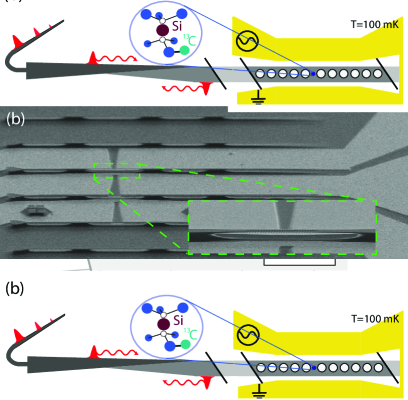
Two recent experiments showcasing the potential of color centers in diamond as quantum network node candidates can be seen in Fig. 3, together defining the state of the art in quantum networks. Fig. 3(a) shows a laboratory-scale quantum network based on nitrogen-vacancy (NV) centers in diamond Pompili et al. (2021). Three NV centers in separate cryostats, linked via optical fiber channels in a line configuration, are operated as independent quantum network nodes. The centers are set to a common optical emission frequency via electric field tuning (DC Stark shift) Bernien et al. (2013). The network is used to demonstrate distribution of three-partite Greenberger-Horne-Zeilinger (GHZ) entangled states across the nodes, as well as entanglement swapping to achieve any-to-any connectivity in the network Pompili et al. (2021). This network sets the state of the art for entanglement-based quantum networks.
Entanglement between the nodes is generated using a photon-emission-based scheme, in which spin-photon entanglement is locally generated at each NV node using microwave and laser pulses. The photonic modes are then interfered on a beam splitter, thereby erasing the which-path information. Subsequent photon detection heralds the generation of a spin-spin entangled state between two NV nodes Bernien et al. (2013); Humphreys et al. (2018). Early experiments Bernien et al. (2013) had employed two-photon entangling schemes reaching fidelities Hensen et al. (2015) at mHz rates. More recent experiments (including the three-node network discussed here) used a single-photon scheme Humphreys et al. (2018) yielding fidelities at rates of HzPompili et al. (2021).
Importantly, these schemes generate entanglement in a heralded fashion, making the fidelity robust to photon loss and the generated entangled states available for further use. In the vicinity of the NV center, a 13C nuclear spin is used as a memory qubit at the middle node, coupled to the NV center electron spin via the hyperfine interaction. The nuclear spin is controlled via tailored microwave pulses applied to the NV center spin Taminiau et al. (2014) that simultaneously decouple the NV electron spin from the other nuclear spins. Characterization of the nuclear spin environment of an NV center has enabled communication qubit coherence times above one second Abobeih et al. (2018). In addition, entangled states have been stored in 13C memory qubits for up to subsequent entanglement generation attempts Reiserer et al. (2016); Kalb et al. (2018); Pompili et al. (2021). Combined with the demonstrated capability of entanglement distillation (generating one higher fidelity state from two lower fidelity states) Kalb et al. (2017) and deterministic entanglement delivery (by generating entanglement between two nodes faster than it is lost, albeit not under full network activity) Humphreys et al. (2018), these experiments highlight the potential of the NV center as a quantum network node. As we discuss in detail below, a main challenge for the NV center is the low fraction of emitted and detected coherent photons, limiting the entanglement rates.
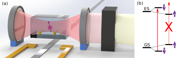
Recently, a new class of defect centers in diamond has also gathered the attention of the community: the family of group-IV color centers in diamond, of which the negatively charged silicon-vacancy (SiV) center is the most studied member. Fig. 3(b) shows a schematic of a SiV center embedded in a photonic crystal cavity, which increases the interaction of light with the communication qubit as compared to emission in a bulk diamond material (discussed in Sec. VI below). Spin-photon entanglement with fidelity 94 % has been generated in this system using cavity quantum electrodynamics (cQED) reflection-based schemes, in which photons impinging on the cavity containing the communication qubit are reflected or transmitted depending on the spin-state of the communication qubit Nguyen et al. (2019b). While entanglement between distant SiV centers has not yet been demonstrated, strong collective interactions between two SiV centers Evans et al. (2018) in the same cavity and probabilistic entanglement generation between two SiVs Sipahigil et al. (2016); Machielse et al. (2019) in one waveguide have been observed. In addition, photon outcoupling efficiencies from the emitter-cavity system into fiber 0.9 have enabled the demonstration of memory-enhanced quantum communication Bhaskar et al. (2020). This experiment sets the state of the art for quantum repeater experiments.
Additionally, recent experiments have demonstrated key quantum network node capabilities, including dynamical decoupling of the SiV spin from the bath with coherence times above 1 ms Sukachev et al. (2017); Nguyen et al. (2019a), 13C nuclear spin initialization, control, and readout via the central SiV electron spin Metsch et al. (2019); Nguyen et al. (2019c), and frequency control of SiV centers via strain tuning Sohn et al. (2018); Machielse et al. (2019); Wan et al. (2020). Combined with recent efforts to fabricate SiV centers in nanophotonic waveguides at a large scale and their integration in photonic circuits Wan et al. (2020), these results show the potential of silicon-vacancy centers and other closely related group-IV color centers as nodes for a quantum network (see Sec. VI).
IV Optical and spin properties of color centers in diamond
Nitrogen-vacancy and group-IV color centers in diamond feature different structural symmetries, which result in different properties of their spin-photon interface. Here, we briefly introduce the most important differences between those color centers in diamond, to the point necessary to understand current limitations and research directions described in the remains of this article; we refer the reader to the many excellent articles that cover the physics of these color centers in great detail Doherty et al. (2013); Hepp (2014); Bradac et al. (2019). In this article, we consider all color centers to be in the negative charge state, except where indicated differently; this negative charge state is the one most commonly studied and used in experiments geared towards entanglement generation.
| Vacancy | ZPL | Quantum | Debye-Waller | Radiative | Ground state splitting | |
|---|---|---|---|---|---|---|
| wavelength [nm] | efficiency [%] | factor | Lifetime [ns] | [GHz] | [K] | |
| SiV | 737 Bhaskar et al. (2020) | Neu, Agio, and Becher (2012); Sipahigil et al. (2016) / Riedrich-Möller et al. (2014) | Neu et al. (2011); Dietrich et al. (2014) | Rogers et al. (2014); Sipahigil et al. (2016) | Hepp et al. (2014); Rogers et al. (2014); Pingault et al. (2017) | 0.1 |
| GeV | Iwasaki et al. (2015) | Høy Jensen et al. (2020); Nguyen et al. (2019d) | Siyushev et al. (2017) | Iwasaki et al. (2015); Bhaskar et al. (2017) | Siyushev et al. (2017) | 0.4 |
| SnV | Iwasaki et al. (2017); Trusheim et al. (2020) | Iwasaki et al. (2017) | Görlitz et al. (2020) | Tchernij et al. (2017); Trusheim et al. (2020); Rugar et al. (2021) | Iwasaki et al. (2017); Trusheim et al. (2020) | 1.8 |
| PbV | Trusheim et al. (2019) | not known | not known | Trusheim et al. (2019) | 5700 Trusheim et al. (2019) | 9.8 |
| NV | Doherty et al. (2013) | Radko et al. (2016) | Faraon et al. (2011); Riedel et al. (2017) | Faraon et al. (2011); Kalb et al. (2018); Ruf et al. (2021) | not applicable | not applicable |
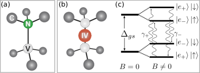
Fig. 4 shows the difference in atomic structure of nitrogen-vacancy (NV) centers and group-IV color centers (consisting of silicon-vacancy (SiV) Hepp et al. (2014); Pingault et al. (2017); Nguyen et al. (2019c), germanium-vacancy (GeV) Siyushev et al. (2017), tin-vacancy (SnV) Iwasaki et al. (2017); Trusheim et al. (2020) and lead-vacancy (PbV) Trusheim et al. (2019) centers). An NV center is formed by a nitrogen atom replacing a carbon atom of the diamond lattice, next to a lattice vacancy, giving rise to a C symmetry [Fig. 4(a)]. The NV center possesses a permanent electric dipole moment, making the optical transition frequencies sensitive to charge fluctuations in its environment Doherty et al. (2013). This sensitivity to electric fields has been used as a resource to tune different NV centers onto resonance Bernien et al. (2012), counteracting local strain inhomogeneities in the host diamond crystal which shift the transition frequencies of color centers. However, it has also hindered the nanophotonic integration of NV centers due to degradation of their optical properties near surfaces Faraon et al. (2012); Ruf et al. (2019).
The NV center features an outstanding spin energy relaxation time of over 8 h Astner et al. (2018). Quantum states have been stored in the NV center’s electronic spin for over one second by decoupling the electron from unwanted interactions in its environment using tailored microwave pulse sequences Abobeih et al. (2018). Fidelities in quantum networks experiments have reached for single qubit gates and for two-qubit gates (between NV electron and 13C nuclear spins) Pompili et al. (2021).
For group-IV color centers, the group-IV atom takes an interstitial lattice site between two lattice vacancies. The resulting inversion-symmetric D structure of the defect [Fig. 4(b)] results in no permanent electric dipole and thus a first-order insensitivity to electric field fluctuations. As a consequence, tuning optical transition frequencies of group-IV color centers by electric fields is relatively inefficient De Santis et al. (2021); Aghaeimeibodi et al. (2021), potentially necessitating other techniques (discussed in Sec. VI below). On the other hand, the vanishing permanent electric dipole makes these color centers excellent candidates for integration into photonic nanostructures (also discussed in Sec. VI below).
Group-IV emitters also feature a different level structure than the NV center: both optical ground and excited states are formed by doubly-degenerate orbital states, which are each split into pairs by spin-orbit interaction and the Jahn-Teller effect. Under an external magnetic field, the double spin degeneracy in each pair () is lifted Hepp et al. (2014); Hepp (2014); Thiering and Gali (2018). The qubit subspace can then for example be defined over the two opposing spin sublevels of the optical ground state’s lower orbital branch [see Fig. 4(c)]. This, however, means that direct microwave driving of the qubit levels is forbidden in first order, as one would need to flip both spin and orbital quantum numbers. Typically, this complication is overcome by working with emitters with transversal strain , which mixes the orbital levels, such that the qubit state can be effectively described by the spin only and thus be driven with higher efficiency Nguyen et al. (2019c). Coherent microwave control of group-IV color centers has recently been demonstrated for SiV centers Sukachev et al. (2017); Nguyen et al. (2019c), with infidelities on the percent level Sukachev et al. (2017). For other group-IV color centers, only incoherent microwave driving of spin transitions has been achieved so far Siyushev et al. (2017); Trusheim et al. (2020). The reported infidelities for coherent SiV control are a result of qubit dephasing during microwave pulses, as relatively low Rabi frequencies ( 10 MHz) are used to limit heating-induced decoherence. It is expected that the use of superconducting waveguides Sigillito et al. (2014) will further improve microwave pulse fidelities (as a result of potentially significantly reduced ohmic heating) for all color centers.
Spin dephasing in the group-IV qubit subspace is dominated by phonon-assisted transitions to the upper ground state orbital branch, which leads to the acquisition of a random phase: while the phonon transitions are in principle spin-conserving, the detuning between the spin states varies depending on which orbital state is occupied, see Fig. 4(c) Jahnke et al. (2015); Meesala et al. (2018). In Tab. 1, we map reported ground state splittings into a concrete performance metric by extrapolating the temperatures below which we expect an orbital coherence time ms due to low phonon occupation. From this, we see that a larger ground state splitting (associated with stronger spin-orbit coupling strengths for heavier ions) is beneficial for maintaining long qubit coherence. However, this requires higher microwave driving powers for similar off-axis strain values, as the strain-induced orbital mixing is related to the spin-orbit coupling strength, and thus the overlap between orbital states is reduced Nguyen et al. (2019c). All-optical spin control schemes represent an alternative to microwave driving, as demonstrated e.g. for SiV Rogers et al. (2014); Pingault et al. (2014); Becker et al. (2018) and GeV Siyushev et al. (2017) centers. For SnV centers, spin initialization by optical pumping has been observed Trusheim et al. (2020). Another way of defining and driving a qubit could be to mix the (mostly) orthogonal spin components via an off-axis magnetic field, and use surface acoustic waves to drive phonon transitions between the orbital levels, with demonstrated Rabi frequencies 30 MHz Maity et al. (2020). Such an off-axis magnetic field, however, is at odds with achieving the high spin cyclicity needed for single shot spin state readout and high fidelity entanglement generation, necessitating a careful tradeoff Nguyen et al. (2019c). For magnetic fields aligned with the color center’s symmetry axis, readout fidelities above 99.99% have been achieved Sukachev et al. (2017); Nguyen et al. (2019b).
Tab. 1 also shows a comparison of the most important optical properties for both group-IV color centers and nitrogen-vacancy centers in diamond. To generate entanglement, only the fraction of coherent photons emitted in the zero-phonon-line (ZPL, for which no lattice vibrations assist the transition Doherty et al. (2013)) can be used Bernien et al. (2013). Importantly, all quantified zero-phonon-line emission fractions for group-IV color centers are significantly larger than for the NV center, as the inversion symmetry of these emitters causes their excited states to have greater overlap with the optical ground state Thiering and Gali (2018), resulting in a higher fraction of direct photon transitions Franck and Dymond (1926); Condon (1926). While most recent quantum memory experiments with SiV centers have operated in dilution refrigerators (see below) in order to suppress thermal phonon population Sukachev et al. (2017); Becker et al. (2018), the SnV center with relatively high expected operating temperature requirements might be particularly promising for use as quantum network node. We note that the neutral charge state variants of group-IV color centers are also promising, as they potentially combine the favorable spin-photon interface of negative group-IV color centers with the excellent spin coherence times and easy qubit manipulation of negative nitrogen vacancy centers Green et al. (2017); Rose et al. (2018); Thiering and Gali (2018); Green et al. (2019); Zhang et al. (2020). We do not discuss it extensively here due to its early stage of study.
V Enhancing the memory qubits
We now discuss the state of the art and future research directions regarding the memory qubits of color centers in diamond. The most common isotope of carbon is 12C. However, the 13C isotope with natural abundance of about carries a nuclear spin of 1/2. In the past decade, techniques have been developed (mostly on NV-based systems) to control these nuclear spins via the position-dependent hyperfine coupling. Universal nuclear spin control using electron decoupling sequences that are on resonance with a single 13C spin has been demonstrated Taminiau et al. (2014). This has enabled the demonstration of coherence times above 10 seconds, and electron-nuclear gate fidelities for individual 13C spins in NV-based systems Kalb et al. (2017); Bradley et al. (2019). Additionally, up to one memory qubit per communication node has been used in an NV-based quantum network setting to date Kalb et al. (2017); Pompili et al. (2021). For the case of SiV centers (and group-IV color centers in general), on the other hand, the spin-half nature of the system leads to a vanishing first-order sensitivity of decoupling sequences to individual 13C hyperfine parameters, thus requiring long decoupling times (and / or potentially off-axis magnetic fields that are at odds with a high spin cyclicity of optical transitions) to isolate out single nuclear spins. So far, electron-nuclear gate fidelities have been limited to for SiV centers Nguyen et al. (2019b); 13C nuclear spins close to group-IV color centers have not yet been used in quantum networks experiments.
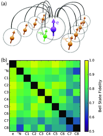
A first area of research is thus to extend the number of available nuclear spin qubits per network node, as well as their control speeds and fidelities. Recently developed gate schemes based on interleaving radiofrequency (RF) driving of 13C nuclear spins (to control previously unaddressable qubits) with dynamical decoupling pulses (to decouple from the spin bath) have allowed the creation of a local quantum register of an NV communication qubit and up to 9 surrounding nuclear spin qubits [see Fig. 5(top)] that allow entangled state generation between all pairs of qubits [Fig. 5(bottom)], creation of a local 7-qubit GHZ state, as well as memory coherence times of single and two qubit states of over ten seconds Bradley et al. (2019). This result (achieved on a similar device as used for distant entanglement generation Bernien et al. (2013); Kalb et al. (2017); Pompili et al. (2021)) shows that it is realistic to expect diamond-based quantum nodes containing many qubits in the near-term future. Such registers could enable scalable, modular quantum computation Nickerson, Fitzsimons, and Benjamin (2014) and universal, fault-tolerant error correction Taminiau et al. (2014); Waldherr et al. (2014); Cramer et al. (2016); Abobeih (2021). Additionally, we expect that RF driving of nuclear spins will overcome current limitations in manipulating nuclear spins for group-IV color centers, as the nuclear spin transition frequencies depend on the hyperfine parameters on first order in this case Nguyen et al. (2019c). Overcoming issues related to sample heating and background amplifier noise could then also enable to address multiple nuclear spins simultaneously, thus reducing decoherence associated with long gate times Bradley et al. (2019). Additionally, cross-talk between nuclear spins, as well as unwanted coupling to other spins could be reduced when using the full information of the environment of a color center Abobeih et al. (2019) (potentially acquired while involving automated techniques Jung et al. (2021)) to simulate and tailor gate sequences for a specific spin environment, and computationally optimizing them for overall protocol fidelity. Another way of extending the number of controllable nuclear spin qubits per node is to also employ the nuclear spin of a nuclear spin containing color center atom isotope, e.g. of 14N (nuclear spin of 1) Pfaff et al. (2014) or 29Si (nuclear spin of 1/2) Pingault et al. (2017).
A second research direction is to increase the coherence time per available memory qubit under full network activity (in particular entanglement generation). The "always-on" nature of the hyperfine interaction of 13C nuclear spin memory qubits and the NV center has limited memory coherence in quantum networks to 500 entanglement generation attempts Kalb et al. (2018); Pompili et al. (2021). Uncontrolled electron dynamics, which result for instance from control infidelities and stochastic electron spin initialization during an entangling sequence, cause dephasing of the nuclear spin memory qubits Kalb et al. (2018). Techniques such as higher magnetic fields at the color center location can speed up gate times and shorten the entanglement generation element, thus reducing the time over which random phases can be picked up Kalb et al. (2018); Pompili et al. (2021). Additionally, decoupling pulses on the memory qubits that suppress quasi-static noise in the environment have shown initial promise to prolong nuclear memory qubit coherence under network activity for NV centers Kalb et al. (2018). Other promising routes to extend the nuclear spin memory coherence time involve reducing the color center’s state-dependent coupling strength (the main dephasing channel), e.g. by employing decoherence-protected subspaces (formed from two or more individual spins, or pairs of strongly-coupled spins that mostly cancel the state-dependent hyperfine interaction term) Reiserer et al. (2016); Abobeih et al. (2018); Bartling et al. (2021), and using isotopically purified samples for which weakly coupled 13C nuclear spin qubits can be controlled Pfender et al. (2017, 2019)). Other methods are to engineer systems of coupled defects (e.g. involving a 13C nuclear spin qubit coupled to a P1 center in the vicinity of an NV center Degen et al. (2020), or to use the nitrogen nuclear spin of a second NV center (whose nitrogen nuclear spin is used as a memory) in proximity to the communicator NV center Yamamoto et al. (2013); Degen (2021).
VI Enhancing the spin-photon interface
Optically-mediated entanglement generation with high rates requires quantum network nodes with efficient spin-photon interfaces. However, the relatively high refractive index of diamond () leads to significant total internal reflection at the diamond-air interface, which limits photon collection efficiencies. Entanglement rates are further reduced by the finite fraction of photons emitted into the zero-phonon line (ZPL) that can be used for entanglement generation (see Sec. IV above). Thus, techniques that can increase the fraction of collected photons at ZPL wavelengths, and / or increase the interaction of light with the emitter are required. Here, we discuss both strategies, as well as their suitability for enhancing the spin-photon interface of different diamond color centers, and the state of the art and future avenues for this research. We note that strong light-matter interactions also open the door to entangling schemes alternative from the photon-emission-based protocols discussed above Cabrillo et al. (1999); Barrett and Kok (2005), e.g. based on spin-dependent cavity reflections Sørensen and Mølmer (2003); Duan and Kimble (2004); Reiserer and Rempe (2015); Bhaskar et al. (2020); Chen, Bersin, and Englund (2021).
VI.1 Strategies for enhancing the spin-photon interface
The two most common strategies to enhance the spin-photon interface are by increasing the photon flux at the detector through improvements in photon collection, and through cavity or Purcell enhancement, which increases light-matter interaction and spontaneous emission rates (see Fig. 6). Here, we only give a brief overview of these methods, and refer to the many extensive diamond-color-center specific review articles that cover them in detail, see e.g. Refs. Schröder et al. (2016); Johnson, Dolan, and Smith (2017); Bradac et al. (2019); Janitz, Bhaskar, and Childress (2020).
VI.1.1 Collection efficiency enhancement
A common method to enhance collection efficiency from color centers in diamond is to fabricate dome-shaped solid immersion lenses around the emitters [Fig. 6(a)], which leads to a higher fraction of light being collected, as total internal reflection is avoided by the light striking the diamond surface at a perpendicular angle. These devices have been used to increase emission from NV Hadden et al. (2010); Marseglia et al. (2011); Robledo et al. (2011); Jamali et al. (2014); Riedel et al. (2014), SiV Hepp et al. (2014); Rogers et al. (2014), and GeV Siyushev et al. (2017); Chen et al. (2019a) centers; all diamond-based remote entanglement generation experiments reported to date have used these devices, with detection efficiencies of emitted photons of up to 10% Robledo et al. (2011).
A second class of collection efficiency enhancement methods is based on nanostructures that modify the far-field emission of a dipole emitter. These structures comprise different dimensions, designs, and supported wavelength ranges, and include parabolic reflectors Wan et al. (2018); Hedrich et al. (2020) [Fig. 6(b)], nanopillars Maletinsky et al. (2012), nanowires Hausmann et al. (2010); Babinec et al. (2010), nanocones Jeon et al. (2020), gratings Choy et al. (2013); Li et al. (2015a) and diamond waveguides Burek et al. (2012); Momenzadeh et al. (2015); Shields et al. (2015); Mouradian et al. (2015); Patel et al. (2016); Sipahigil et al. (2016); Bhaskar et al. (2017); Rugar et al. (2020a); Wan et al. (2020) [Fig. 6(c)]. While they offer large-scale fabrication and higher collection efficiencies than solid immersion lenses (reported dipole-waveguide coupling efficiencies above 55% Hedrich et al. (2020); Wan et al. (2020)), the demands in nano-fabrication and color center placement are more stringent than for solid-immersion lenses, and emitters have to be brought in close proximity to nano-fabricated surfaces. This proximity to surfaces is believed to be the cause of optical instability for some diamond color centers, as discussed in detail below. Such instabilities make it challenging to produce indistinguishable photons from remote centers as required for entanglement generation Legero et al. (2003, 2006).
VI.1.2 Purcell enhancement
Another way of enhancing the spin-photon interface is to embed the dipole emitter inside an optical cavity, making use of the Purcell effect, described by a Purcell factor . This factor scales with the ratio of the cavity quality factor, (inversely proportional to the cavity’s energy decay rate), to the cavity mode volume, (describing the cavity light field confinement) Reiserer and Rempe (2015). Briefly, a cavity enhances the density of states around its resonance frequency, such that the spontaneous emission of an embedded dipole emitter is increased when on resonance with the cavity following Fermi’s golden rule. Additionally, the cavity funnels emitted light into a well-defined mode that can be readily matched e.g. to that of optical fibers. A commonly used parameter to quantify the radiative emission enhancement by the cavity (defined as the ratio of the dipole-cavity emission, , compared to the emission in a homogeneous medium, ) is the cooperativity, , defined as
| (1) |
where is the dipole-cavity coupling rate, is the energy decay rate from the cavity, is the free-space radiative emitter decay rate, is the non-radiative emitter decay rate, is the fraction of photon emission from the emitter into the zero-phonon line (given by the Debye-Waller factor), and is the quantum efficiency (defined as the ratio of radiative to all decay). While this quantifies the efficiency of the spin-photon interface, it does not take into account the coherence of the emitter: in practice, solid state emitters often experience dephasing due to unwanted interactions with the environment of the solid state host, characterized by a pure dephasing rate , which manifests in broadening of the optical transitions above the lifetime limited value Robledo et al. (2010); Santori et al. (2010); Riedel et al. (2017); Jantzen et al. (2016); Nguyen et al. (2019b); Rugar et al. (2020a). Therefore, it is useful to introduce the coherent cooperativity, , which quantifies the ratio of coherent decay into the cavity mode to undesired decay, and is given as Borregaard, Sørensen, and Lodahl (2019); Janitz, Bhaskar, and Childress (2020)
| (2) |
can be interpreted as the probability of coherent atom-photon interaction, and plays an important role in the fidelity and efficiency of many near-deterministic quantum protocols (which require ) Borregaard, Sørensen, and Lodahl (2019).
To date, cavity enhancement of diamond color centers has been demonstrated for different implementations, including diamond-on-insulator whispering gallery mode resonators Faraon et al. (2011); Hausmann et al. (2012) and nanodiamond plasmonic antennas Bogdanov et al. (2020). Another class of devices are based on the coupling of non-diamond resonators to color centers in nanodiamonds Wolters et al. (2010); Van Der Sar et al. (2011); Fehler et al. (2019, 2020) or diamond films Englund et al. (2010); Barclay et al. (2011); Gould et al. (2016). Open and tunable micro-cavities geometries have also been demonstrated for embedded nanodiamonds Albrecht et al. (2013); Kaupp et al. (2013); Albrecht et al. (2014); Johnson et al. (2015); Kaupp et al. (2016); Benedikter et al. (2017) and thin diamond membranes Riedel et al. (2017); Høy Jensen et al. (2020); Häußler et al. (2019); Salz et al. (2020); Ruf et al. (2021) [Fig. 6(d)]. Steady progress in diamond nanofabrication has also led to all-diamond photonic crystal cavities Faraon et al. (2012); Hausmann et al. (2013); Li et al. (2015b); Riedrich-Möller et al. (2015); Sipahigil et al. (2016); Schröder et al. (2017); Evans et al. (2018); Jung et al. (2019); Nguyen et al. (2019b, c); Bhaskar et al. (2020)[Fig. 6(e)], with demonstrated coherent cooperativities exceeding 100 for the case of the SiV center Bhaskar et al. (2020).
Quantum network applications also require the efficient coupling of light from these nanostructures to optical fibers. Different methods of coupling to fiber-based communication channels have been realized to date, including optimized free-space couplers with efficiencies up to Dory et al. (2019); Rugar et al. (2020a), notch couplers with efficiencies Sipahigil et al. (2016), grating couplers with efficiencies Hausmann et al. (2012); Rath et al. (2013), and double- Khanaliloo et al. (2015a); Patel et al. (2016); Mitchell, Lake, and Barclay (2019) and single- Burek et al. (2017); Nguyen et al. (2019c); Evans et al. (2018); Bhaskar et al. (2020) sided fiber-tapers with efficiencies of up to .
VI.2 Looking forward: key challenges and potential solutions
Having introduced different theoretical concepts to increase the spin-photon interface of color centers in diamond, we now discuss the experimental state of the art of such enhancement, highlighting key challenges and potential research directions.
VI.2.1 NV centers
While the nitrogen-vacancy (NV) center has been a workhorse of quantum network demonstrations with color centers in diamond, its low fraction of optical emission at the zero-phonon line (ZPL) frequency of 3%, as well as limited collection efficiency from solid immersion lenses currently restrict local entanglement generation rates to <100 Hz Humphreys et al. (2018); Pompili et al. (2021). Due to their permanent electric dipole moment, NV centers experience large spectral shifts on short timescales caused by charge fluctuations in the environment when close to surfaces ( microns) Ruf et al. (2019). As a result, despite reported Purcell factors of up to 70 in small mode-volume photonic crystal cavities Faraon et al. (2012), the regime of has remained out of reach. We note that the origins of the surface noise are still a subject of active research, and that recent experiments geared at understanding the effect and origins of surface noise on the NV center spin Bluvstein, Zhang, and Jayich (2019), and the local electrostatic environment of NV centers Sangtawesin et al. (2019) show promise towards understanding the causes of surface charge noise. Combined with proposals for active optical driving to reduce spectral diffusion effects Fotso et al. (2016), this could revive the field of NV centers in nanophotonic structures in the future.
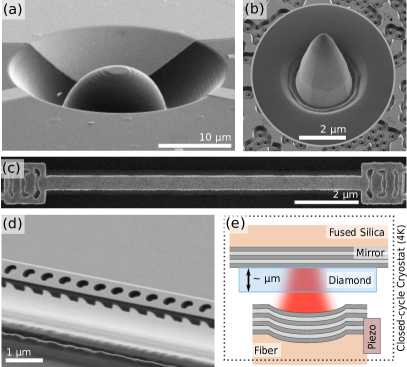
The challenge imposed by nearby surfaces can be circumvented by embedding microns-thin diamond membranes between two highly reflective mirrors Janitz et al. (2015). A recently reported fabrication technique has formed NV centers with bulk-like optical properties in -thin diamond membranes that can be embedded in such cavities via a combination of electron irradiation, high temperature annealing, and a tailored diamond etching sequence Ruf et al. (2019) [Fig. 7(a)]. This has allowed for the first demonstration of resonant excitation and detection of optically coherent NV centers, Purcell enhanced by an optical cavity Ruf et al. (2021), as would be required for cavity-enhanced entanglement generation. However, the Purcell enhancement in this experiment was limited to , (mostly) due to cavity-length fluctuations 100 pm induced by a closed-cycle cryocooler. Previously, it has been shown (using off-resonant excitation) that Purcell enhancement factors of up to 30 (corresponding to 46% of light emitted in the ZPL) can be achieved for such open micro-cavities in a liquid helium bath cryostat (featuring lower cavity length fluctuations) Riedel et al. (2017) [Fig. 7(b)]. Combined, these experiments demonstrate that there is a near-term path from the current towards and coherent photon collection efficiencies . In addition, recent results suggest that it should be possible to reach the required pm-scale cavity length fluctuations even in closed-cycle cryostats Merkel, Ulanowski, and Reiserer (2020); Fontana et al. (2021), which would remove the need for a liquid helium infrastructure at each quantum network node.
Another active area of research is to create shallow, stable NV centers Lekavicius, Oo, and Wang (2019); Kasperczyk et al. (2020); Yurgens et al. (2021) at controlled locations; both the electron irradiation technique employed in Ref. Ruf et al. (2021), as well as recently introduced laser-writing techniques Chen et al. (2019b) can form optically coherent NV centers, but rely on native nitrogen in the sample to recombine with introduced lattice vacancies and thus miss precise control of the site of NV center formation. However, for maximal Purcell enhancement, NV centers should be positioned at an antinode of the cavity field. While such precision can be achieved using ion implantation, recent research has shown that NV centers created via this technique suffer from increased optical linewidths compared to NV centers formed during growth van Dam et al. (2019), even after extended high temperature treatments to restore the diamond lattice Chu et al. (2014).
While it will remain challenging to achieve coherent cooperativites (and thereby enter the near-deterministic spin-photon interface regime Borregaard, Sørensen, and Lodahl (2019)), the open cavity approach is projected to speed up current emission-based entanglement generation schemes by 2 orders of magnitude Ruf et al. (2021). This could allow for continuous deterministic entanglement generation (generating high fidelity entanglement faster than it is lost), and enable experiments such as the formation of a quantum repeater surpassing direct transmission Rozpȩdek et al. (2019), and device-independent quantum key distribution Murta et al. (2019) using NV centers.
VI.2.2 Group-IV color centers
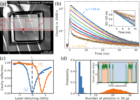
The first-order electric field insensitivity of group-IV color centers in diamond Sipahigil et al. (2014); Evans et al. (2016); Thiering and Gali (2018); Müller et al. (2014); Iwasaki et al. (2015); Tchernij et al. (2017); Trusheim et al. (2020); Rugar et al. (2020a); Trusheim et al. (2019) has enabled the demonstration of close-to-lifetime limited optical transitions even in heavily fabricated nanophotonic structures Evans et al. (2016); Sipahigil et al. (2016); Bhaskar et al. (2017); Nguyen et al. (2019c); Rugar et al. (2020a); Wan et al. (2020). To date, photonic crystal cavity coupling of group-IV color centers in diamond at low temperatures has been demonstrated for SiV Sipahigil et al. (2016); Evans et al. (2018); Nguyen et al. (2019b, c); Bhaskar et al. (2020) and SnV centers Rugar et al. (2021), with demonstrated for the case of the SiV center Bhaskar et al. (2020). This system allows for spin-state dependent photon reflection, enabling high fidelity single shot spin state readout with demonstrated fidelities [see Fig. 7(c,d)]. This has recently enabled the first demonstration of memory-enhanced quantum communication Bhaskar et al. (2020).
A key requirement for many remote entanglement generation schemes is the ability to tune two group-IV color centers located on separate chips to a common resonance frequency. So far, tuning the emission frequency of group-IV emitters has been demonstrated using strain Meesala et al. (2018); Sohn et al. (2018); Maity et al. (2018); Machielse et al. (2019); Wan et al. (2020), electric fields De Santis et al. (2021); Aghaeimeibodi et al. (2021), and Raman-type Sipahigil et al. (2016); Sun et al. (2018) schemes (although the latter is only compatible with emission-based entanglement generation schemes), but only for single emitters, or several emitters in one structure. The first two tuning techniques deform the orbitals of the group-IV color centers, and thus the color’s inversion symmetry is broken, leading to an observed increase in transition linewidths and spectral diffusion under applied external strain / electric field (potentially due to an increase in sensitivity to charge noise in the environment). We note that recent experiments indicate a larger tuning range of transitions for strain tuning (as compared to electric field tuning) for the same induced line broadening Wan et al. (2020); De Santis et al. (2021); Aghaeimeibodi et al. (2021).
While close-to-lifetime limited linewidths of group-IV color centers in nanophotonic structures have been observed, experiments still routinely show spectral shifts and charge instabilities, leading to broadening several lifetime-limited linewidths Evans et al. (2018); Nguyen et al. (2019c); Rugar et al. (2020a); Wan et al. (2020), as well as large local strain fields. While dynamic strain tuning can be used to suppress slow spectral diffusion (seconds timescale) Machielse et al. (2019), it is challenging to improve the homogeneous linewidth (sub-microsecond timescale) that enters the coherent cooperativity using this approach. Typically, emitters are created by high-energy implantation, followed by a high temperature annealing step to form group-IV vacancy centers and to reduce the effects of lattice damage from the implantation process Chu et al. (2014). However, there is evidence that even such high temperature treatments can not fully recover the original diamond lattice van Dam et al. (2019). A recently developed promising method to overcome this limitation employs low energy shallow ion implantation, combined with overgrowth of diamond material Rugar et al. (2020b). Another strategy could be to combine low-density ion implantation with electron irradiation, to reduce the amount of damage created in the lattice via the (heavy) ion implantation McLellan et al. (2016). Combined with controlled engineering of the diamond Fermi level Collins (2002); Rose et al. (2018); Murai et al. (2018), these techniques could increase the quality and stability of group-IV color center optical transitions Tchernij et al. (2017); Evans et al. (2018); Nguyen et al. (2019c); Trusheim et al. (2019); Rugar et al. (2020a); Wan et al. (2020).
Another area of active development involves the design and fabrication of the nanophotonic structures. Despite recent progress Schreck et al. (2017); Nelz et al. (2019), growing high quality, thin film diamond on large scales is challenging, and (to the best of our knowledge) there is no wet processing technique that can etch bulk single-crystal diamond along its crystal planes, thus requiring either laborious thinning of diamond on a low index material, or sophisticated techniques to produce suspended, wavelength-thick diamond devices. While initial research focused on creating sub--thin diamond films via selectively wet-etching a localized graphitized diamond layer Parikh et al. (1992); Fairchild et al. (2008); Gaathon et al. (2013); Lee et al. (2014); Piracha et al. (2016a, b) or etching down a super-polished thin diamond membrane Faraon et al. (2012); Hausmann et al. (2013); Riedrich-Möller et al. (2014); Li et al. (2015b); Cady et al. (2019), these methods typically feature low device yield (as a consequence of challenges in device handling and initial material thickness variations). Thus, recent research has focused on fabricating structures directly in commercially available bulk diamond material via a combination of a hard mask and an angled diamond etch (leading to a triangular device cross-section) Burek et al. (2012); Bayn et al. (2014); Burek et al. (2014); Sipahigil et al. (2016); Atikian et al. (2017); Zhang et al. (2018); Nguyen et al. (2019c), or a quasi-isotropic (dry) undercut etch, which selectively etches along certain diamond crystal planes (leading to rectangular device cross-section) Khanaliloo et al. (2015b, c); Mouradian et al. (2017); Wan, Mouradian, and Englund (2018); Dory et al. (2019); Zheng et al. (2019); Wan et al. (2020). Known limitations to these processes include mixing of TE- and TM-like modes that will ultimately limit device quality factors for triangular devices, as well as a relatively high bottom surface roughness for quasi-isotropic etched devices (although it is worthwhile to note that the fabrication parameter space is somewhat less explored for the latter technique).
Currently, all listed fabrication methods routinely achieve photonic crystal cavity quality factors , about two orders of magnitude lower than simulated values Mouradian et al. (2017). These deviations are caused by a combination of surface roughness Nguyen et al. (2019c), non-uniform hole sizes Rugar et al. (2021), and deviations from the expected device cross-section Wan, Mouradian, and Englund (2018); we expect that an order-of-magnitude improvement in device quality factors is within reach upon further optimization. Furthermore, although photonic crystal nanocavities can be designed and fabricated to resonate at the ZPL frequency, they are especially sensitive to process variations, leading to a resonance wavelength spread of 5 nm across devices Mouradian et al. (2017). Nonetheless, this spread in frequency may be overcome by cavity tuning methods Mosor et al. (2005); Faraon et al. (2012); Sipahigil et al. (2016), which are in any case needed for the precise overlapping of the ZPL and cavity frequency.
As nanofabrication methods are constantly refined, it is also likely that current methods of optimally aligning color centers within nanophotonic structures (to guarantee maximal overlap between the optical mode and the dipole emitter) can be further improved. Towards this end, various methods have already been demonstrated, including the targeted fabrication around pre-located centers Wan et al. (2018), or ion implantation into devices using either masks Nguyen et al. (2019c) or focused implantation Sipahigil et al. (2016); Wan et al. (2020). Compared to the SiV center for which has been demonstrated, GeV and SnV centers have intrinsically higher radiative efficiencies and thus potentially higher cooperativities, which may increase cavity-QED-based protocol fidelities (see discussion below).
We note that group-IV color centers in diamond are also suitable for integration into tuneable, open micro-cavities, as recently demonstrated for GeV Høy Jensen et al. (2020) and SiV Häußler et al. (2019); Salz et al. (2020) centers at room temperature. It should be possible to achieve for these systems, potentially providing a viable alternative to the more fabrication-intensive nanostructures.
VII Towards large-scale quantum networks
Having discussed the core quantum network components based on diamond color centers, we now turn to what is required to build these into a network capable of distributing entanglement over large distances at high rates.
First, a future quantum internet will likely make use of existing fiber infrastructure. This necessitates the matching of the photon wavelength from the network node to the telecommunication bands using quantum frequency conversion. Recently, it has been demonstrated that spin-photon entanglement can be preserved after frequency down-conversion of a nm photon entangled with the spin-state of the NV center to telecommunication wavelengths ( nm) Tchebotareva et al. (2019). Similar conversion techniques can be applied to other color centers and quantum systems Krutyanskiy et al. (2019); Bock et al. (2018); Ikuta et al. (2018); Yu et al. (2020); De Greve et al. (2012). Future work will focus on increasing the system efficiency and potentially integrating on-chip conversion (see below).
Second, future quantum networks covering large distances will require many quantum repeater stations –– each with a large number of qubits –– for multiplexing, purification and error-correction. For example, 5-10 repeater stations with kilohertz entangled bit (ebit) rates need a total of data qubits to reach mega-ebits per second communication Muralidharan et al. (2016). Although color center devices are already produced using standard nanofabrication techniques, the needed scale for high-rate, high-fidelity networks would require large-scale manufacturing of quantum nodes. This task not only entails qubit and device production but also the packaging of efficient optical and microwave signals to and from many independent color centers at once.
Optical technologies such as photonic integrated circuits (PICs) may play an important role in addressing these challenges. Their programmability Bogaerts et al. (2020) and access to a large number of spatial modes Harris et al. (2018) are especially of interest to quantum network applications. Similar to their bulk optics counterparts, PICs comprise of low-loss on-chip components, such as waveguides, filters and switches. References Bogaerts et al. (2020); Blumenthal et al. (2018); Harris et al. (2018); Zhu et al. (2021) review the device concepts and state of the art of PIC technologies that may be relevant to quantum network applications. Driven by foundry adoption, as well as new frontiers in data communication Sun et al. (2015); Atabaki et al. (2018), photonic processors Wetzstein et al. (2020); Shastri et al. (2021) and optical quantum computing Wang et al. (2020), integrated photonic circuits have advanced dramatically in manufacturability and complexity over the last decade. The first notable feature of PICs for quantum technologies is their compact footprint, which not only promotes dense integration, but also reduces phase errors in quantum interference of photons Bogaerts et al. (2020). Next, phase modulators in PICs can implement on-chip switches for routing photons within an optical network Bogaerts et al. (2020), and material nonlinearities can be used for efficient frequency conversion between visible and telecommunication photons Wang et al. (2018). Finally, multi-channel optical access can be accomplished using standard fiber arrays, and electrical packaging for large-scale control of color centers can be achieved using potential metal layers in a PIC stack.
Photonic circuits in diamond have been previously demonstrated for opto-mechanics Rath et al. (2013) and nonlinear optics Hausmann et al. (2014). Gallium phosphide-on-diamond photonics have also been used to route the emission from NV centers Gould et al. (2016). However, the non-deterministic creation and integration of color centers in devices, as well as the absence of single-crystal diamond wafers have limited the scale of diamond integrated photonics (see Sec. VI). One way to combine the functionalities and performance of industry-leading photonic circuits with diamond is through heterogeneous integration of diamond with other material systems. Also known as "hybrid photonics" Kim et al. (2020); Elshaari et al. (2020), this approach is akin to modern integrated circuits in that discrete chips are separately optimized and fabricated and then populated into a larger circuit board. Examples of heterogeneous integration include modulators and lasers in silicon photonics Komljenovic et al. (2018). In the context of quantum photonics, recent successes include quantum emitters Kim et al. (2020); Elshaari et al. (2020) and single-photon detectors Najafi et al. (2015), which are otherwise difficult to achieve in a single material platform with high performance.
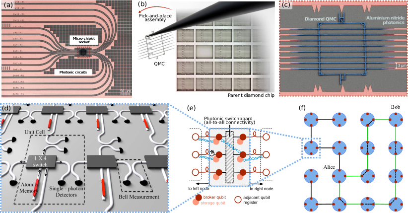
Heterogeneous integration of diamond color centers with PICs circumvents the yield issues associated with all-diamond architectures, thereby allowing potentially many addressable qubits within a single chip. A recent result showing the large-scale integration of color centers in diamond with hybrid photonic integrated circuits Wan et al. (2020) is shown in Fig. 8(a-c). Diamond quantum micro-chiplets, each consisting of 8 diamond nanophotonic waveguides with at least one addressable group-IV color center, are integrated with PICs based on aluminum nitride [Fig. 8(c)]. After fabrication using the quasi-isotropic undercut technique (see Sec. VI), a total of 16 chiplets numbering to 128 waveguides were positioned with sub-microns accuracy on the PIC [Fig. 8(a)] using a pick-and-place technique [Fig. 8(b)]. The coupling of the color center to the waveguide can be as high as 55 %, and the diamond-PIC coupling and PIC-to-optical fiber coupling are reported to be 34 % and 11 %, respectively. In addition, electrodes in this hybrid PIC enabled the in-situ tuning of optical transition frequencies within this integrated device architecture Wan et al. (2020). The availability of multiple color centers per waveguide potentially allows for spectral multiplexing Bersin et al. (2019); Chen et al. (2020), which is a hardware-efficient path to multiplying the total number of qubits to , where and are the number of spatial and frequency channels, respectively.
With further improvements in waveguide-emitter coupling as well as diamond-nanocavity integration with PICs, such a hybrid architecture could become an important building block of future quantum network nodes. Looking forward, we expect future developments to also focus on integrating chip components for color center technologies, such as CMOS-integrated microwave electronics for spin control Kim et al. (2019), on-chip beamsplitters for photon quantum interference Wang et al. (2020), optical switches for channel connectivity Bogaerts et al. (2020), single-photon detectors Reithmaier et al. (2015); Najafi et al. (2015); Schwartz et al. (2018); Gyger et al. (2021) for heralded entanglement, and quantum frequency conversion Guo et al. (2016); Jankowski et al. (2020) or frequency tuning Hu et al. (2020) on the same microphotonic platform. While these functionalities have been realized in other PIC platforms, a key challenge is to bring together various technologies and materials for implementing a chip-based node. Here, the advances in heterogeneous integration will be critical for controlling and deploying a large number of such chips.
As an example of such a chip, Fig. 8(d) shows a modular architecture with many unit cells per network node Choi et al. (2019). Each unit cell consists of atomic memories, photonic switches, and single-photon detectors. The atomic memories include communication qubits for inter-cell entanglement and memory qubits for long-term storage and intracell information processing. The switching network selects one of the adjacent cells, and the photo-detectors herald successful entanglement events between cells. Such a photonic architecture could allow for entanglement routing within a chip-based node, potentially boosting the communication rate Duan and Kimble (2004); Lee et al. (2020). By establishing connectivity between unit cells using optical switches, the resulting network is scalable because adding nodes does not require any modification in the existing network.
Once multiple long-lived memory qubits that can be controlled with high fidelity are available per quantum network node, the entanglement fidelity can be greatly improved through entanglement distillation (purification), where low fidelity entangled pairs are employed as a resource and transformed to a smaller number of high fidelity pairs after local operations and classical communication Bennett et al. (1996); Deutsch et al. (1996). Such a scheme has recently been demonstrated in a proof-of-principle experiment between two distant NV centers that each have access to an additional 13C memory Kalb et al. (2017). While such distillation requires additional time resources as a result from two-way-classical-communication, quantum error correction Jiang et al. (2009) can achieve a more favorable key rate per qubit scalingMuralidharan et al. (2016). Such error correction can be performed if the operational error is smaller than the threshold of a given code (e.g. for the Calderbank-Shor-Stean (CSS) code Poulin (2006)). If the photon-loss of a link is sufficiently small, heralded entanglement generation can also be replaced with error correction, allowing to move beyond two-way signalling associated with the heralding Borregaard et al. (2020). In addition, multi-qubit network nodes can be operated in a way that outperforms more simple linear repeater schemes. For example, Fig. 8(f) shows a 2D network with nearest-neighbor connectivity that allows multi-path entanglement routing Pant et al. (2019). Crucially, the algorithm only requires local knowledge about which of the entanglement generation attempts with its nearest neighbor succeeded while still achieving faster key distribution than a linear repeater chain Pant et al. (2019).
VIII Conclusions
We have provided a perspective on the emerging field of quantum networks based on diamond color centers. Diamond color centers already define the state of the art in multi-node entanglement-based networks Pompili et al. (2021) and in memory-enhanced quantum key distribution Bhaskar et al. (2020). We expect the next years to see rapid progress on photonic interfaces and integration of color centers, paving the way for first experiments on long-distance quantum links. From the basic building blocks, larger-scale devices will be designed and constructed. Control layers of higher abstraction – akin to the current Internet – are currently being developed Dahlberg et al. (2019); Pirker and Dür (2019).
A future functional quantum network will support many interesting applications, such as distributed quantum computing Cuomo, Caleffi, and Cacciapuoti (2020), accessing a quantum server in the cloud with full privacy Broadbent, Fitzsimons, and Kashefi (2009) and stabilizing quantum clocks Hodges et al. (2013); Kómár et al. (2014). Color centers in diamond may play an essential role in these networks, as the “satisfactory repeater”, or perhaps the “transistor of the quantum age.”
Acknowledgements
We thank Ben Dixon, Mihir Bhaskar, Eric Bersin, Johannes Borregaard, Tim Taminiau, Matteo Pompili, and Matteo Pasini for feedback on the manuscript, Hans Beukers for the calculations of operation temperatures of color centers, and Matteo Pompili, Mihir Bhaskar, Christian Nguyen, Daniel Riedel, Alison Rugar, Shahriar Aghaeimeibodi, Conor Bradley, Mihir Pant, Yuan Lee, Michael Burek and Cleaven Chia for providing originals of figures. D.E. acknowledges support from Brookhaven National Laboratory, which is supported by the U.S. Department of Energy, Office of Basic Energy Sciences, under Contract No. DE-SC0012704. N.W. acknowledges support from the MITRE Quantum Moonshot initiative. H.C. acknowledges the Claude E. Shannon Fellowship and Samsung Scholarship. R.H. and M.R. acknowledge financial support from the EU Flagship on Quantum Technologies through the project Quantum Internet Alliance, from the Netherlands Organisation for Scientific Research (NWO) through a VICI grant and the Zwaartekracht program Quantum Software Consortium, and the European Research Council (ERC) through a Consolidator Grant.
References
- Gertner (2012) J. Gertner, The Idea Factory (Penguin, New York, 2012).
- Park (1970) J. L. Park, “The concept of transition in quantum mechanics,” Foundations of Physics 1, 23–33 (1970).
- Kimble (2008) H. J. Kimble, “The quantum internet,” Nature 453, 1023–1030 (2008).
- Wehner, Elkouss, and Hanson (2018) S. Wehner, D. Elkouss, and R. Hanson, “Quantum internet : A vision for the road ahead,” Science 362, 303 (2018).
- Pirandola et al. (2017) S. Pirandola, R. Laurenza, C. Ottaviani, and L. Banchi, “Fundamental limits of repeaterless quantum communications,” Nature Communications 8, 1–15 (2017).
- Briegel et al. (1998) H.-J. Briegel, W. Dür, J. I. Cirac, and P. Zoller, “Quantum Repeaters: The Role of Imperfect Local Operations in Quantum Communication,” Physical Review Letters 81, 5932–5935 (1998).
- Cabrillo et al. (1999) C. Cabrillo, J. I. Cirac, P. García-Fernández, and P. Zoller, “Creation of entangled states of distant atoms by interference,” Physical Review A 59, 1025–1033 (1999).
- Barrett and Kok (2005) S. D. Barrett and P. Kok, “Efficient high-fidelity quantum computation using matter qubits and linear optics,” Physical Review A 71, 060310 (2005).
- Duan and Kimble (2004) L. M. Duan and H. J. Kimble, “Scalable photonic quantum computation through cavity-assisted interactions,” Physical Review Letters 92, 1–4 (2004).
- Delteil et al. (2016) A. Delteil, Z. Sun, W. B. Gao, E. Togan, S. Faelt, and A. Imamoglu, “Generation of heralded entanglement between distant hole spins,” Nature Physics 12, 218–223 (2016).
- Stockill et al. (2017) R. Stockill, M. J. Stanley, L. Huthmacher, E. Clarke, M. Hugues, A. J. Miller, C. Matthiesen, C. Le Gall, and M. Atatüre, “Phase-Tuned Entangled State Generation between Distant Spin Qubits,” Physical Review Letters 119, 1–6 (2017).
- Moehring et al. (2007) D. L. Moehring, P. Maunz, S. Olmschenk, K. C. Younge, D. N. Matsukevich, L. M. Duan, and C. Monroe, “Entanglement of single-atom quantum bits at a distance,” Nature 449, 68–71 (2007).
- Hucul et al. (2015) D. Hucul, I. V. Inlek, G. Vittorini, C. Crocker, S. Debnath, S. M. Clark, and C. Monroe, “Modular entanglement of atomic qubits using photons and phonons,” Nature Physics 11, 37–42 (2015).
- Stephenson et al. (2020) L. J. Stephenson, D. P. Nadlinger, B. C. Nichol, S. An, P. Drmota, T. G. Ballance, K. Thirumalai, J. F. Goodwin, D. M. Lucas, and C. J. Ballance, “High-Rate, High-Fidelity Entanglement of Qubits Across an Elementary Quantum Network,” Physical Review Letters 124, 1–6 (2020).
- Ritter et al. (2012) S. Ritter, C. Nölleke, C. Hahn, A. Reiserer, A. Neuzner, M. Uphoff, M. Mücke, E. Figueroa, J. Bochmann, and G. Rempe, “An elementary quantum network of single atoms in optical cavities,” Nature 484, 195–200 (2012).
- Hofmann et al. (2012) J. Hofmann, M. Krug, N. Ortegel, L. Gérard, M. Weber, W. Rosenfeld, and H. Weinfurter, “Heralded Entanglement Between Widely Separated Atoms,” Science 337, 72–75 (2012).
- Daiss et al. (2021) S. Daiss, S. Langenfeld, S. Welte, E. Distante, P. Thomas, L. Hartung, O. Morin, and G. Rempe, “A quantum-logic gate between distant quantum-network modules,” Science 371, 614–617 (2021).
- Langenfeld et al. (2021) S. Langenfeld, S. Welte, L. Hartung, S. Daiss, P. Thomas, O. Morin, E. Distante, and G. Rempe, “Quantum Teleportation between Remote Qubit Memories with Only a Single Photon as a Resource,” Physical Review Letters 126, 130502 (2021).
- Bernien et al. (2013) H. Bernien, B. Hensen, W. Pfaff, G. Koolstra, M. S. Blok, L. Robledo, T. H. Taminiau, M. Markham, D. J. Twitchen, L. Childress, and R. Hanson, “Heralded entanglement between solid-state qubits separated by three metres,” Nature 497, 86–90 (2013).
- Hensen et al. (2015) B. Hensen, H. Bernien, A. E. Dréau, A. Reiserer, N. Kalb, M. S. Blok, J. Ruitenberg, R. F. Vermeulen, R. N. Schouten, C. Abellán, W. Amaya, V. Pruneri, M. W. Mitchell, M. Markham, D. J. Twitchen, D. Elkouss, S. Wehner, T. H. Taminiau, and R. Hanson, “Loophole-free Bell inequality violation using electron spins separated by 1.3 kilometres,” Nature 526, 682–686 (2015).
- Bhaskar et al. (2017) M. K. Bhaskar, D. D. Sukachev, A. Sipahigil, R. E. Evans, M. J. Burek, C. T. Nguyen, L. J. Rogers, P. Siyushev, M. H. Metsch, H. Park, F. Jelezko, M. Lončar, and M. D. Lukin, “Quantum Nonlinear Optics with a Germanium-Vacancy Color Center in a Nanoscale Diamond Waveguide,” Physical Review Letters 118, 223603 (2017).
- Nguyen et al. (2019a) C. T. Nguyen, D. D. Sukachev, M. K. Bhaskar, B. Machielse, D. S. Levonian, E. N. Knall, P. Stroganov, R. Riedinger, H. Park, M. Lončar, and M. D. Lukin, “Quantum Network Nodes Based on Diamond Qubits with an Efficient Nanophotonic Interface,” Physical Review Letters 123, 1–6 (2019a).
- Bhaskar et al. (2020) M. K. Bhaskar, R. Riedinger, B. Machielse, D. S. Levonian, C. T. Nguyen, E. N. Knall, H. Park, D. Englund, M. Lončar, D. D. Sukachev, and M. D. Lukin, “Experimental demonstration of memory-enhanced quantum communication,” Nature 580, 60–64 (2020).
- Trusheim et al. (2020) M. E. Trusheim, B. Pingault, N. H. Wan, M. Gündoǧan, L. De Santis, R. Debroux, D. Gangloff, C. Purser, K. C. Chen, M. Walsh, J. J. Rose, J. N. Becker, B. Lienhard, E. Bersin, I. Paradeisanos, G. Wang, D. Lyzwa, A. R. Montblanch, G. Malladi, H. Bakhru, A. C. Ferrari, I. A. Walmsley, M. Atatüre, and D. Englund, “Transform-Limited Photons from a Coherent Tin-Vacancy Spin in Diamond,” Physical Review Letters 124, 1–6 (2020).
- Nagy et al. (2019) R. Nagy, M. Niethammer, M. Widmann, Y.-C. Chen, P. Udvarhelyi, C. Bonato, J. U. Hassan, R. Karhu, I. G. Ivanov, N. T. Son, J. R. Maze, T. Ohshima, Ö. O. Soykal, Á. Gali, S.-Y. Lee, F. Kaiser, and J. Wrachtrup, “High-fidelity spin and optical control of single silicon-vacancy centres in silicon carbide,” Nature Communications 10, 1954 (2019).
- Bourassa et al. (2020) A. Bourassa, C. P. Anderson, K. C. Miao, M. Onizhuk, H. Ma, A. L. Crook, H. Abe, J. Ul-Hassan, T. Ohshima, N. T. Son, G. Galli, and D. D. Awschalom, “Entanglement and control of single nuclear spins in isotopically engineered silicon carbide,” Nature Materials , 1–7 (2020).
- Lukin, Guidry, and Vučković (2020) D. M. Lukin, M. A. Guidry, and J. Vučković, “Integrated Quantum Photonics with Silicon Carbide: Challenges and Prospects,” PRX Quantum 1, 020102 (2020).
- Raha et al. (2020) M. Raha, S. Chen, C. M. Phenicie, S. Ourari, A. M. Dibos, and J. D. Thompson, “Optical quantum nondemolition measurement of a single rare earth ion qubit,” Nature Communications 11, 1–6 (2020).
- Kindem et al. (2020) J. M. Kindem, A. Ruskuc, J. G. Bartholomew, J. Rochman, Y. Q. Huan, and A. Faraon, “Control and single-shot readout of an ion embedded in a nanophotonic cavity,” Nature 580, 201–204 (2020).
- Merkel, Ulanowski, and Reiserer (2020) B. Merkel, A. Ulanowski, and A. Reiserer, “Coherent and Purcell-Enhanced Emission from Erbium Dopants in a Cryogenic High-Q Resonator,” Physical Review X 10, 041025 (2020).
- Chu and Gröblacher (2020) Y. Chu and S. Gröblacher, “A perspective on hybrid quantum opto- and electromechanical systems,” Applied Physics Letters 117, 150503 (2020).
- Mirhosseini et al. (2020) M. Mirhosseini, A. Sipahigil, M. Kalaee, and O. Painter, “Superconducting qubit to optical photon transduction,” Nature 588, 599–603 (2020).
- Forsch et al. (2020) M. Forsch, R. Stockill, A. Wallucks, I. Marinković, C. Gärtner, R. A. Norte, F. van Otten, A. Fiore, K. Srinivasan, and S. Gröblacher, “Microwave-to-optics conversion using a mechanical oscillator in its quantum ground state,” Nature Physics 16, 69–74 (2020).
- Hease et al. (2020) W. Hease, A. Rueda, R. Sahu, M. Wulf, G. Arnold, H. G. Schwefel, and J. M. Fink, “Bidirectional Electro-Optic Wavelength Conversion in the Quantum Ground State,” PRX Quantum 1, 1 (2020).
- Krastanov et al. (2020) S. Krastanov, H. Raniwala, J. Holzgrafe, K. Jacobs, M. Lončar, M. J. Reagor, and D. R. Englund, “Optically-Heralded Entanglement of Superconducting Systems in Quantum Networks,” arXiv , 1–8 (2020), arXiv:2012.13408 .
- Kalb et al. (2017) N. Kalb, A. A. Reiserer, P. C. Humphreys, J. J. Bakermans, S. J. Kamerling, N. H. Nickerson, S. C. Benjamin, D. J. Twitchen, M. Markham, and R. Hanson, “Entanglement distillation between solid-state quantum network nodes,” Science 356, 928–932 (2017).
- Pompili et al. (2021) M. Pompili, S. L. N. Hermans, S. Baier, H. K. C. Beukers, P. C. Humphreys, R. N. Schouten, R. F. L. Vermeulen, M. J. Tiggelman, L. dos Santos Martins, B. Dirkse, S. Wehner, and R. Hanson, “Realization of a multinode quantum network of remote solid-state qubits,” Science 372, 259–264 (2021).
- Nickerson, Fitzsimons, and Benjamin (2014) N. H. Nickerson, J. F. Fitzsimons, and S. C. Benjamin, “Freely scalable quantum technologies using cells of 5-to-50 qubits with very lossy and noisy photonic links,” Physical Review X 4, 1–17 (2014).
- Choi et al. (2019) H. Choi, M. Pant, S. Guha, and D. Englund, “Percolation-based architecture for cluster state creation using photon-mediated entanglement between atomic memories,” npj Quantum Information 5, 104 (2019).
- Gottesman, Jennewein, and Croke (2012) D. Gottesman, T. Jennewein, and S. Croke, “Longer-baseline telescopes using quantum repeaters,” Physical Review Letters 109, 1–5 (2012).
- Kómár et al. (2014) P. Kómár, E. M. Kessler, M. Bishof, L. Jiang, A. S. Sørensen, J. Ye, and M. D. Lukin, “A quantum network of clocks,” Nature Physics 10, 582–587 (2014).
- Ekert and Renner (2014) A. Ekert and R. Renner, “The ultimate physical limits of privacy,” Nature 507, 443–447 (2014).
- Humphreys et al. (2018) P. C. Humphreys, N. Kalb, J. P. Morits, R. N. Schouten, R. F. Vermeulen, D. J. Twitchen, M. Markham, and R. Hanson, “Deterministic delivery of remote entanglement on a quantum network,” Nature 558, 268–273 (2018).
- Taminiau et al. (2014) T. H. Taminiau, J. Cramer, T. Van Der Sar, V. V. Dobrovitski, and R. Hanson, “Universal control and error correction in multi-qubit spin registers in diamond,” Nature Nanotechnology 9, 171–176 (2014).
- Abobeih et al. (2018) M. H. Abobeih, J. Cramer, M. A. Bakker, N. Kalb, M. Markham, D. J. Twitchen, and T. H. Taminiau, “One-second coherence for a single electron spin coupled to a multi-qubit nuclear-spin environment,” Nature Communications 9, 1–8 (2018).
- Reiserer et al. (2016) A. Reiserer, N. Kalb, M. S. Blok, K. J. M. van Bemmelen, T. H. Taminiau, R. Hanson, D. J. Twitchen, and M. Markham, “Robust Quantum-Network Memory Using Decoherence-Protected Subspaces of Nuclear Spins,” Physical Review X 6, 021040 (2016).
- Kalb et al. (2018) N. Kalb, P. C. Humphreys, J. J. Slim, and R. Hanson, “Dephasing mechanisms of diamond-based nuclear-spin memories for quantum networks,” Physical Review A 97, 062330 (2018).
- Nguyen et al. (2019b) C. T. Nguyen, D. D. Sukachev, M. K. Bhaskar, B. MacHielse, D. S. Levonian, E. N. Knall, P. Stroganov, R. Riedinger, H. Park, M. Lončar, and M. D. Lukin, “Quantum Network Nodes Based on Diamond Qubits with an Efficient Nanophotonic Interface,” Physical Review Letters 123, 1–6 (2019b).
- Evans et al. (2018) R. E. Evans, M. K. Bhaskar, D. D. Sukachev, C. T. Nguyen, A. Sipahigil, M. J. Burek, B. Machielse, G. H. Zhang, A. S. Zibrov, E. Bielejec, H. Park, M. Lončar, and M. D. Lukin, “Photon-mediated interactions between quantum emitters in a diamond nanocavity,” Science 362, 662–665 (2018).
- Sipahigil et al. (2016) A. Sipahigil, R. E. Evans, D. D. Sukachev, M. J. Burek, J. Borregaard, M. K. Bhaskar, C. T. Nguyen, J. L. Pacheco, H. A. Atikian, C. Meuwly, R. M. Camacho, F. Jelezko, E. Bielejec, H. Park, M. Lončar, and M. D. Lukin, “An integrated diamond nanophotonics platform for quantum-optical networks,” Science 354, 847–850 (2016).
- Machielse et al. (2019) B. Machielse, S. Bogdanovic, S. Meesala, S. Gauthier, M. J. Burek, G. Joe, M. Chalupnik, Y. I. Sohn, J. Holzgrafe, R. E. Evans, C. Chia, H. Atikian, M. K. Bhaskar, D. D. Sukachev, L. Shao, S. Maity, M. D. Lukin, and M. Lončar, “Quantum Interference of Electromechanically Stabilized Emitters in Nanophotonic Devices,” Physical Review X 9, 1–11 (2019).
- Sukachev et al. (2017) D. D. Sukachev, A. Sipahigil, C. T. Nguyen, M. K. Bhaskar, R. E. Evans, F. Jelezko, and M. D. Lukin, “Silicon-Vacancy Spin Qubit in Diamond: A Quantum Memory Exceeding 10 ms with Single-Shot State Readout,” Physical Review Letters 119, 223602 (2017).
- Metsch et al. (2019) M. H. Metsch, K. Senkalla, B. Tratzmiller, J. Scheuer, M. Kern, J. Achard, A. Tallaire, M. B. Plenio, P. Siyushev, and F. Jelezko, “Initialization and Readout of Nuclear Spins via a Negatively Charged Silicon-Vacancy Center in Diamond,” Physical Review Letters 122, 190503 (2019).
- Nguyen et al. (2019c) C. T. Nguyen, D. D. Sukachev, M. K. Bhaskar, B. MacHielse, D. S. Levonian, E. N. Knall, P. Stroganov, C. Chia, M. J. Burek, R. Riedinger, H. Park, M. Lončar, and M. D. Lukin, “An integrated nanophotonic quantum register based on silicon-vacancy spins in diamond,” Physical Review B 100, 1–19 (2019c).
- Sohn et al. (2018) Y. I. Sohn, S. Meesala, B. Pingault, H. A. Atikian, J. Holzgrafe, M. Gündoǧan, C. Stavrakas, M. J. Stanley, A. Sipahigil, J. Choi, M. Zhang, J. L. Pacheco, J. Abraham, E. Bielejec, M. D. Lukin, M. Atatüre, and M. Lončar, “Controlling the coherence of a diamond spin qubit through its strain environment,” Nature Communications 9, 17–22 (2018).
- Wan et al. (2020) N. H. Wan, T. J. Lu, K. C. Chen, M. P. Walsh, M. E. Trusheim, L. De Santis, E. A. Bersin, I. B. Harris, S. L. Mouradian, I. R. Christen, E. S. Bielejec, and D. Englund, “Large-scale integration of artificial atoms in hybrid photonic circuits,” Nature 583, 226–231 (2020).
- Doherty et al. (2013) M. W. Doherty, N. B. Manson, P. Delaney, F. Jelezko, J. Wrachtrup, and L. C. Hollenberg, “The nitrogen-vacancy colour centre in diamond,” Physics Reports 528, 1–45 (2013).
- Hepp (2014) C. Hepp, “Electronic structure of the silicon vacancy color center in diamond,” Ph.D. thesis, Saarland University (2014).
- Bradac et al. (2019) C. Bradac, W. Gao, J. Forneris, M. E. Trusheim, and I. Aharonovich, “Quantum nanophotonics with group IV defects in diamond,” Nature Communications 10, 5625 (2019).
- Neu, Agio, and Becher (2012) E. Neu, M. Agio, and C. Becher, “Photophysics of single silicon vacancy centers in diamond: implications for single photon emission,” Optics Express 20, 19956 (2012).
- Riedrich-Möller et al. (2014) J. Riedrich-Möller, C. Arend, C. Pauly, F. Mücklich, M. Fischer, S. Gsell, M. Schreck, and C. Becher, “Deterministic Coupling of a Single Silicon-Vacancy Color Center to a Photonic Crystal Cavity in Diamond,” Nano Letters 14, 5281–5287 (2014).
- Neu et al. (2011) E. Neu, D. Steinmetz, J. Riedrich-Möller, S. Gsell, M. Fischer, M. Schreck, and C. Becher, “Single photon emission from silicon-vacancy colour centres in chemical vapour deposition nano-diamonds on iridium,” New Journal of Physics 13, 0–21 (2011).
- Dietrich et al. (2014) A. Dietrich, K. D. Jahnke, J. M. Binder, T. Teraji, J. Isoya, L. J. Rogers, and F. Jelezko, “Isotopically varying spectral features of silicon-vacancy in diamond,” New Journal of Physics 16, 113019 (2014).
- Rogers et al. (2014) L. Rogers, K. Jahnke, T. Teraji, L. Marseglia, C. Müller, B. Naydenov, H. Schauffert, C. Kranz, J. Isoya, L. McGuinness, and F. Jelezko, “Multiple intrinsically identical single-photon emitters in the solid state,” Nature Communications 5, 4739 (2014).
- Hepp et al. (2014) C. Hepp, T. Müller, V. Waselowski, J. N. Becker, B. Pingault, H. Sternschulte, D. Steinmüller-Nethl, A. Gali, J. R. Maze, M. Atatüre, and C. Becher, “Electronic Structure of the Silicon Vacancy Color Center in Diamond,” Physical Review Letters 112, 036405 (2014).
- Pingault et al. (2017) B. Pingault, D. D. Jarausch, C. Hepp, L. Klintberg, J. N. Becker, M. Markham, C. Becher, and M. Atatüre, “Coherent control of the silicon-vacancy spin in diamond,” Nature Communications 8, 1–7 (2017).
- Iwasaki et al. (2015) T. Iwasaki, F. Ishibashi, Y. Miyamoto, Y. Doi, S. Kobayashi, T. Miyazaki, K. Tahara, K. D. Jahnke, L. J. Rogers, B. Naydenov, F. Jelezko, S. Yamasaki, S. Nagamachi, T. Inubushi, N. Mizuochi, and M. Hatano, “Germanium-Vacancy Single Color Centers in Diamond,” Scientific Reports 5, 1–7 (2015).
- Høy Jensen et al. (2020) R. Høy Jensen, E. Janitz, Y. Fontana, Y. He, O. Gobron, I. P. Radko, M. Bhaskar, R. Evans, C. D. Rodríguez Rosenblueth, L. Childress, A. Huck, and U. Lund Andersen, “Cavity-Enhanced Photon Emission from a Single Germanium-Vacancy Center in a Diamond Membrane,” Physical Review Applied 13, 064016 (2020).
- Nguyen et al. (2019d) M. Nguyen, N. Nikolay, C. Bradac, M. Kianinia, E. A. Ekimov, N. Mendelson, O. Benson, and I. Aharonovich, “Photodynamics and quantum efficiency of germanium vacancy color centers in diamond,” Advanced Photonics 1, 1 (2019d).
- Siyushev et al. (2017) P. Siyushev, M. H. Metsch, A. Ijaz, J. M. Binder, M. K. Bhaskar, D. D. Sukachev, A. Sipahigil, R. E. Evans, C. T. Nguyen, M. D. Lukin, P. R. Hemmer, Y. N. Palyanov, I. N. Kupriyanov, Y. M. Borzdov, L. J. Rogers, and F. Jelezko, “Optical and microwave control of germanium-vacancy center spins in diamond,” Physical Review B 96, 081201 (2017).
- Iwasaki et al. (2017) T. Iwasaki, Y. Miyamoto, T. Taniguchi, P. Siyushev, M. H. Metsch, F. Jelezko, and M. Hatano, “Tin-Vacancy Quantum Emitters in Diamond,” Physical Review Letters 119, 253601 (2017).
- Görlitz et al. (2020) J. Görlitz, D. Herrmann, G. Thiering, P. Fuchs, M. Gandil, T. Iwasaki, T. Taniguchi, M. Kieschnick, J. Meijer, M. Hatano, A. Gali, and C. Becher, “Spectroscopic investigations of negatively charged tin-vacancy centres in diamond,” New Journal of Physics 22, 013048 (2020).
- Tchernij et al. (2017) S. D. Tchernij, T. Herzig, J. Forneris, J. Küpper, S. Pezzagna, P. Traina, E. Moreva, I. P. Degiovanni, G. Brida, N. Skukan, M. Genovese, M. Jakšić, J. Meijer, and P. Olivero, “Single-Photon-Emitting Optical Centers in Diamond Fabricated upon Sn Implantation,” ACS Photonics 4, 2580–2586 (2017).
- Rugar et al. (2021) A. E. Rugar, S. Aghaeimeibodi, D. Riedel, C. Dory, H. Lu, P. J. McQuade, Z.-X. Shen, N. A. Melosh, and J. Vučković, “A Quantum Photonic Interface for Tin-Vacancy Centers in Diamond,” , 1–7 (2021), arXiv:2102.11852 .
- Trusheim et al. (2019) M. E. Trusheim, N. H. Wan, K. C. Chen, C. J. Ciccarino, J. Flick, R. Sundararaman, G. Malladi, E. Bersin, M. Walsh, B. Lienhard, H. Bakhru, P. Narang, and D. Englund, “Lead-related quantum emitters in diamond,” Physical Review B 99, 1–7 (2019).
- Radko et al. (2016) I. P. Radko, M. Boll, N. M. Israelsen, N. Raatz, J. Meijer, F. Jelezko, U. L. Andersen, and A. Huck, “Determining the internal quantum efficiency of shallow-implanted nitrogen-vacancy defects in bulk diamond,” Optics Express 24, 27715 (2016).
- Faraon et al. (2011) A. Faraon, P. E. Barclay, C. Santori, K. M. C. Fu, and R. G. Beausoleil, “Resonant enhancement of the zero-phonon emission from a colour centre in a diamond cavity,” Nature Photonics 5, 301–305 (2011).
- Riedel et al. (2017) D. Riedel, I. Söllner, B. J. Shields, S. Starosielec, P. Appel, E. Neu, P. Maletinsky, and R. J. Warburton, “Deterministic enhancement of coherent photon generation from a nitrogen-vacancy center in ultrapure diamond,” Physical Review X 7, 1–8 (2017).
- Ruf et al. (2021) M. Ruf, M. Weaver, S. van Dam, and R. Hanson, “Resonant Excitation and Purcell Enhancement of Coherent Nitrogen-Vacancy Centers Coupled to a Fabry-Perot Microcavity,” Physical Review Applied 15, 024049 (2021).
- Bernien et al. (2012) H. Bernien, L. Childress, L. Robledo, M. Markham, D. Twitchen, and R. Hanson, “Two-Photon Quantum Interference from Separate Nitrogen Vacancy Centers in Diamond,” Physical Review Letters 108, 043604 (2012).
- Faraon et al. (2012) A. Faraon, C. Santori, Z. Huang, V. M. Acosta, and R. G. Beausoleil, “Coupling of Nitrogen-Vacancy Centers to Photonic Crystal Cavities in Monocrystalline Diamond,” Physical Review Letters 109, 033604 (2012).
- Ruf et al. (2019) M. Ruf, M. IJspeert, S. van Dam, N. de Jong, H. van den Berg, G. Evers, and R. Hanson, “Optically Coherent Nitrogen-Vacancy Centers in Micrometer-Thin Etched Diamond Membranes,” Nano Letters 19, 3987–3992 (2019).
- Astner et al. (2018) T. Astner, J. Gugler, A. Angerer, S. Wald, S. Putz, N. J. Mauser, M. Trupke, H. Sumiya, S. Onoda, J. Isoya, J. Schmiedmayer, P. Mohn, and J. Majer, “Solid-state electron spin lifetime limited by phononic vacuum modes,” Nature Materials 17, 313–317 (2018).
- De Santis et al. (2021) L. De Santis, M. Trusheim, K. Chen, and D. Englund, “Investigation of the Stark Effect on a Centrosymmetric Quantum Emitter in Diamond,” , 1–6 (2021), arXiv:2102.01322 .
- Aghaeimeibodi et al. (2021) S. Aghaeimeibodi, D. Riedel, A. E. Rugar, C. Dory, and J. Vuckovic, “Electrical tuning of tin-vacancy centers in diamond,” , 1–8 (2021), arXiv:2103.01917 .
- Thiering and Gali (2018) G. Thiering and A. Gali, “Ab Initio Magneto-Optical Spectrum of Group-IV Vacancy Color Centers in Diamond,” Physical Review X 8, 021063 (2018).
- Sigillito et al. (2014) A. J. Sigillito, H. Malissa, A. M. Tyryshkin, H. Riemann, N. V. Abrosimov, P. Becker, H.-J. Pohl, M. L. W. Thewalt, K. M. Itoh, J. J. L. Morton, A. A. Houck, D. I. Schuster, and S. A. Lyon, “Fast, low-power manipulation of spin ensembles in superconducting microresonators,” Applied Physics Letters 104, 222407 (2014).
- Jahnke et al. (2015) K. D. Jahnke, A. Sipahigil, J. M. Binder, M. W. Doherty, M. Metsch, L. J. Rogers, N. B. Manson, M. D. Lukin, and F. Jelezko, “Electron–phonon processes of the silicon-vacancy centre in diamond,” New Journal of Physics 17, 043011 (2015).
- Meesala et al. (2018) S. Meesala, Y. I. Sohn, B. Pingault, L. Shao, H. A. Atikian, J. Holzgrafe, M. Gündoǧan, C. Stavrakas, A. Sipahigil, C. Chia, R. Evans, M. J. Burek, M. Zhang, L. Wu, J. L. Pacheco, J. Abraham, E. Bielejec, M. D. Lukin, M. Atatüre, and M. Lončar, “Strain engineering of the silicon-vacancy center in diamond,” Physical Review B 97, 1–13 (2018).
- Pingault et al. (2014) B. Pingault, J. N. Becker, C. H. Schulte, C. Arend, C. Hepp, T. Godde, A. I. Tartakovskii, M. Markham, C. Becher, and M. Atatüre, “All-Optical Formation of Coherent Dark States of Silicon-Vacancy Spins in Diamond,” Physical Review Letters 113, 263601 (2014).
- Becker et al. (2018) J. N. Becker, B. Pingault, D. Groß, M. Gündoğan, N. Kukharchyk, M. Markham, A. Edmonds, M. Atatüre, P. Bushev, and C. Becher, “All-Optical Control of the Silicon-Vacancy Spin in Diamond at Millikelvin Temperatures,” Physical Review Letters 120, 053603 (2018).
- Maity et al. (2020) S. Maity, L. Shao, S. Bogdanović, S. Meesala, Y.-I. Sohn, N. Sinclair, B. Pingault, M. Chalupnik, C. Chia, L. Zheng, K. Lai, and M. Lončar, “Coherent acoustic control of a single silicon vacancy spin in diamond,” Nature Communications 11, 193 (2020).
- Franck and Dymond (1926) J. Franck and E. G. Dymond, “Elementary processes of photochemical reactions,” Transactions of the Faraday Society 21, 536 (1926).
- Condon (1926) E. Condon, “A Theory of Intensity Distribution in Band Systems,” Physical Review 28, 1182–1201 (1926).
- Green et al. (2017) B. L. Green, S. Mottishaw, B. G. Breeze, A. M. Edmonds, U. F. S. D’Haenens-Johansson, M. W. Doherty, S. D. Williams, D. J. Twitchen, and M. E. Newton, “Neutral Silicon-Vacancy Center in Diamond: Spin Polarization and Lifetimes,” Physical Review Letters 119, 096402 (2017).
- Rose et al. (2018) B. C. Rose, D. Huang, Z.-H. Zhang, P. Stevenson, A. M. Tyryshkin, S. Sangtawesin, S. Srinivasan, L. Loudin, M. L. Markham, A. M. Edmonds, D. J. Twitchen, S. A. Lyon, and N. P. de Leon, “Observation of an environmentally insensitive solid-state spin defect in diamond,” Science 361, 60–63 (2018).
- Green et al. (2019) B. L. Green, M. W. Doherty, E. Nako, N. B. Manson, U. F. S. D’Haenens-Johansson, S. D. Williams, D. J. Twitchen, and M. E. Newton, “Electronic structure of the neutral silicon-vacancy center in diamond,” Physical Review B 99, 161112 (2019).
- Zhang et al. (2020) Z.-H. Zhang, P. Stevenson, G. Thiering, B. C. Rose, D. Huang, A. M. Edmonds, M. L. Markham, S. A. Lyon, A. Gali, and N. P. de Leon, “Optically Detected Magnetic Resonance in Neutral Silicon Vacancy Centers in Diamond via Bound Exciton States,” Physical Review Letters 125, 237402 (2020).
- Bradley et al. (2019) C. E. Bradley, J. Randall, M. H. Abobeih, R. C. Berrevoets, M. J. Degen, M. A. Bakker, M. Markham, D. J. Twitchen, and T. H. Taminiau, “A Ten-Qubit Solid-State Spin Register with Quantum Memory up to One Minute,” Physical Review X 9, 31045 (2019).
- Waldherr et al. (2014) G. Waldherr, Y. Wang, S. Zaiser, M. Jamali, T. Schulte-Herbrüggen, H. Abe, T. Ohshima, J. Isoya, J. F. Du, P. Neumann, and J. Wrachtrup, “Quantum error correction in a solid-state hybrid spin register,” Nature 506, 204–207 (2014).
- Cramer et al. (2016) J. Cramer, N. Kalb, M. A. Rol, B. Hensen, M. S. Blok, M. Markham, D. J. Twitchen, R. Hanson, and T. H. Taminiau, “Repeated quantum error correction on a continuously encoded qubit by real-time feedback,” Nature Communications 7, 1–7 (2016).
- Abobeih (2021) M. H. Abobeih, “From atomic-scale imaging to quantum fault-tolerance with spins in diamond,” Ph.D. thesis, TU Delft (2021).
- Abobeih et al. (2019) M. H. Abobeih, J. Randall, C. E. Bradley, H. P. Bartling, M. A. Bakker, M. J. Degen, M. Markham, D. J. Twitchen, and T. H. Taminiau, “Atomic-scale imaging of a 27-nuclear-spin cluster using a quantum sensor,” Nature 576, 411–415 (2019).
- Jung et al. (2021) K. Jung, M. H. Abobeih, J. Yun, G. Kim, H. Oh, A. Henry, T. H. Taminiau, and D. Kim, “Deep learning enhanced individual nuclear-spin detection,” npj Quantum Information 7, 41 (2021).
- Pfaff et al. (2014) W. Pfaff, B. J. Hensen, H. Bernien, S. B. Van Dam, M. S. Blok, T. H. Taminiau, M. J. Tiggelman, R. N. Schouten, M. Markham, D. J. Twitchen, and R. Hanson, “Unconditional quantum teleportation between distant solid-state quantum bits,” Science 345, 532–535 (2014).
- Bartling et al. (2021) H. P. Bartling, M. H. Abobeih, B. Pingault, M. J. Degen, S. J. H. Loenen, C. E. Bradley, J. Randall, M. Markham, D. J. Twitchen, and T. H. Taminiau, “Coherence and entanglement of inherently long-lived spin pairs in diamond,” (2021), arXiv:2103.07961 .
- Pfender et al. (2017) M. Pfender, N. Aslam, H. Sumiya, S. Onoda, P. Neumann, J. Isoya, C. A. Meriles, and J. Wrachtrup, “Nonvolatile nuclear spin memory enables sensor-unlimited nanoscale spectroscopy of small spin clusters,” Nature Communications 8, 834 (2017).
- Pfender et al. (2019) M. Pfender, P. Wang, H. Sumiya, S. Onoda, W. Yang, D. B. R. Dasari, P. Neumann, X.-y. Pan, J. Isoya, R.-b. Liu, and J. Wrachtrup, “High-resolution spectroscopy of single nuclear spins via sequential weak measurements,” Nature Communications 10, 594 (2019).
- Degen et al. (2020) M. Degen, S. J. Loenen, H. P. Bartling, C. E. Bradley, A. L. Meinsma, M. Markham, D. J. Twitchen, and T. H. Taminiau, “Entanglement of dark electron-nuclear spin defects in diamond,” arXiv (2020), arXiv:2011.09874 .
- Yamamoto et al. (2013) T. Yamamoto, C. Müller, L. P. McGuinness, T. Teraji, B. Naydenov, S. Onoda, T. Ohshima, J. Wrachtrup, F. Jelezko, and J. Isoya, “Strongly coupled diamond spin qubits by molecular nitrogen implantation,” Physical Review B - Condensed Matter and Materials Physics 88, 1–5 (2013).
- Degen (2021) M. J. Degen, “On the creation, coherence and entanglement of multi-defect quantum registers in diamond,” Ph.D. thesis, TU Delft (2021).
- Sørensen and Mølmer (2003) A. S. Sørensen and K. Mølmer, “Probabilistic Generation of Entanglement in Optical Cavities,” Physical Review Letters 90, 127903 (2003).
- Reiserer and Rempe (2015) A. Reiserer and G. Rempe, “Cavity-based quantum networks with single atoms and optical photons,” Reviews of Modern Physics 87, 1379–1418 (2015).
- Chen, Bersin, and Englund (2021) K. C. Chen, E. Bersin, and D. Englund, “A polarization encoded photon-to-spin interface,” npj Quantum Information 7, 1–6 (2021).
- Schröder et al. (2016) T. Schröder, S. L. Mouradian, J. Zheng, M. E. Trusheim, M. Walsh, E. H. Chen, L. Li, I. Bayn, and D. Englund, “Quantum nanophotonics in diamond,” Journal of the Optical Society of America B 33, B65 (2016).
- Johnson, Dolan, and Smith (2017) S. Johnson, P. R. Dolan, and J. M. Smith, “Diamond photonics for distributed quantum networks,” Progress in Quantum Electronics 55, 129–165 (2017).
- Janitz, Bhaskar, and Childress (2020) E. Janitz, M. K. Bhaskar, and L. Childress, “Cavity quantum electrodynamics with color centers in diamond,” Optica 7, 1232 (2020).
- Hadden et al. (2010) J. P. Hadden, J. P. Harrison, A. C. Stanley-Clarke, L. Marseglia, Y.-L. D. Ho, B. R. Patton, J. L. O’Brien, and J. G. Rarity, “Strongly enhanced photon collection from diamond defect centers under microfabricated integrated solid immersion lenses,” Applied Physics Letters 97, 241901 (2010).
- Marseglia et al. (2011) L. Marseglia, J. P. Hadden, A. C. Stanley-Clarke, J. P. Harrison, B. Patton, Y.-L. D. Ho, B. Naydenov, F. Jelezko, J. Meijer, P. R. Dolan, J. M. Smith, J. G. Rarity, and J. L. O’Brien, “Nanofabricated solid immersion lenses registered to single emitters in diamond,” Applied Physics Letters 98, 133107 (2011).
- Robledo et al. (2011) L. Robledo, L. Childress, H. Bernien, B. Hensen, P. F. A. Alkemade, and R. Hanson, “High-fidelity projective read-out of a solid-state spin quantum register,” Nature 477, 574–578 (2011).
- Jamali et al. (2014) M. Jamali, I. Gerhardt, M. Rezai, K. Frenner, H. Fedder, and J. Wrachtrup, “Microscopic diamond solid-immersion-lenses fabricated around single defect centers by focused ion beam milling,” Review of Scientific Instruments 85, 123703 (2014).
- Riedel et al. (2014) D. Riedel, D. Rohner, M. Ganzhorn, T. Kaldewey, P. Appel, E. Neu, R. J. Warburton, and P. Maletinsky, “Low-loss broadband antenna for efficient photon collection from a coherent spin in diamond,” Physical Review Applied 2, 1–6 (2014).
- Chen et al. (2019a) D. Chen, Z. Mu, Y. Zhou, J. E. Fröch, A. Rasmit, C. Diederichs, N. Zheludev, I. Aharonovich, and W.-b. Gao, “Optical Gating of Resonance Fluorescence from a Single Germanium Vacancy Color Center in Diamond,” Physical Review Letters 123, 033602 (2019a).
- Wan et al. (2018) N. H. Wan, B. J. Shields, D. Kim, S. Mouradian, B. Lienhard, M. Walsh, H. Bakhru, T. Schröder, and D. Englund, “Efficient Extraction of Light from a Nitrogen-Vacancy Center in a Diamond Parabolic Reflector,” Nano Letters 18, 2787–2793 (2018).
- Hedrich et al. (2020) N. Hedrich, D. Rohner, M. Batzer, P. Maletinsky, and B. J. Shields, “Parabolic Diamond Scanning Probes for Single-Spin Magnetic Field Imaging,” Physical Review Applied 14, 064007 (2020).
- Maletinsky et al. (2012) P. Maletinsky, S. Hong, M. S. Grinolds, B. Hausmann, M. D. Lukin, R. L. Walsworth, M. Loncar, and A. Yacoby, “A robust scanning diamond sensor for nanoscale imaging with single nitrogen-vacancy centres,” Nature Nanotechnology 7, 320–324 (2012).
- Hausmann et al. (2010) B. J. M. Hausmann, M. Khan, Y. Zhang, T. M. Babinec, K. Martinick, M. McCutcheon, P. R. Hemmer, and M. Loncar, “Fabrication of diamond nanowires for quantum information processing applications,” Diamond and Related Materials 19, 621–629 (2010).
- Babinec et al. (2010) T. M. Babinec, B. J. Hausmann, M. Khan, Y. Zhang, J. R. Maze, P. R. Hemmer, and M. Lončar, “A diamond nanowire single-photon source,” Nature Nanotechnology 5, 195–199 (2010).
- Jeon et al. (2020) S.-W. Jeon, J. Lee, H. Jung, S.-W. Han, Y.-W. Cho, Y.-S. Kim, H.-T. Lim, Y. Kim, M. Niethammer, W. C. Lim, J. Song, S. Onoda, T. Ohshima, R. Reuter, A. Denisenko, J. Wrachtrup, and S.-Y. Lee, “Bright Nitrogen-Vacancy Centers in Diamond Inverted Nanocones,” ACS Photonics 7, 2739–2747 (2020).
- Choy et al. (2013) J. T. Choy, I. Bulu, B. J. M. Hausmann, E. Janitz, I.-C. Huang, and M. Lončar, “Spontaneous emission and collection efficiency enhancement of single emitters in diamond via plasmonic cavities and gratings,” Applied Physics Letters 103, 161101 (2013).
- Li et al. (2015a) L. Li, E. H. Chen, J. Zheng, S. L. Mouradian, F. Dolde, T. Schröder, S. Karaveli, M. L. Markham, D. J. Twitchen, and D. Englund, “Efficient Photon Collection from a Nitrogen Vacancy Center in a Circular Bullseye Grating,” Nano Letters 15, 1493–1497 (2015a).
- Burek et al. (2012) M. J. Burek, N. P. de Leon, B. J. Shields, B. J. M. Hausmann, Y. Chu, Q. Quan, A. S. Zibrov, H. Park, M. D. Lukin, and M. Lončar, “Free-Standing Mechanical and Photonic Nanostructures in Single-Crystal Diamond,” Nano Letters 12, 6084–6089 (2012).
- Momenzadeh et al. (2015) S. A. Momenzadeh, R. J. Stöhr, F. F. de Oliveira, A. Brunner, A. Denisenko, S. Yang, F. Reinhard, and J. Wrachtrup, “Nanoengineered Diamond Waveguide as a Robust Bright Platform for Nanomagnetometry Using Shallow Nitrogen Vacancy Centers,” Nano Letters 15, 165–169 (2015).
- Shields et al. (2015) B. J. Shields, Q. P. Unterreithmeier, N. P. de Leon, H. Park, and M. D. Lukin, “Efficient Readout of a Single Spin State in Diamond via Spin-to-Charge Conversion,” Physical Review Letters 114, 136402 (2015).
- Mouradian et al. (2015) S. L. Mouradian, T. Schröder, C. B. Poitras, L. Li, J. Goldstein, E. H. Chen, M. Walsh, J. Cardenas, M. L. Markham, D. J. Twitchen, M. Lipson, and D. Englund, “Scalable Integration of Long-Lived Quantum Memories into a Photonic Circuit,” Physical Review X 5, 031009 (2015).
- Patel et al. (2016) R. N. Patel, T. Schröder, N. Wan, L. Li, S. L. Mouradian, E. H. Chen, and D. R. Englund, “Efficient photon coupling from a diamond nitrogen vacancy center by integration with silica fiber,” Light: Science and Applications 5, e16032–e16032 (2016).
- Rugar et al. (2020a) A. E. Rugar, C. Dory, S. Aghaeimeibodi, H. Lu, S. Sun, S. D. Mishra, Z.-X. Shen, N. A. Melosh, and J. Vučković, “Narrow-Linewidth Tin-Vacancy Centers in a Diamond Waveguide,” ACS Photonics 7, 2356–2361 (2020a).
- Legero et al. (2003) T. Legero, T. Wilk, A. Kuhn, and G. Rempe, “Time-resolved two-photon quantum interference,” Applied Physics B: Lasers and Optics 77, 797–802 (2003).
- Legero et al. (2006) T. Legero, T. Wilk, A. Kuhn, and G. Rempe, “Characterization of Single Photons Using Two-Photon Interference,” Advances in Atomic, Molecular and Optical Physics 53, 253–289 (2006).
- Burek et al. (2014) M. J. Burek, Y. Chu, M. S. Z. Liddy, P. Patel, J. Rochman, S. Meesala, W. Hong, Q. Quan, M. D. Lukin, and M. Lončar, “High quality-factor optical nanocavities in bulk single-crystal diamond,” Nature Communications 5, 5718 (2014).
- Burek et al. (2016) M. J. Burek, J. D. Cohen, S. M. Meenehan, N. El-Sawah, C. Chia, T. Ruelle, S. Meesala, J. Rochman, H. A. Atikian, M. Markham, D. J. Twitchen, M. D. Lukin, O. Painter, and M. Lončar, “Diamond optomechanical crystals,” Optica 3, 1404 (2016).
- Robledo et al. (2010) L. Robledo, H. Bernien, I. van Weperen, and R. Hanson, “Control and Coherence of the Optical Transition of Single Nitrogen Vacancy Centers in Diamond,” Physical Review Letters 105, 177403 (2010).
- Santori et al. (2010) C. Santori, P. E. Barclay, K.-M. C. Fu, R. G. Beausoleil, S. Spillane, and M. Fisch, “Nanophotonics for quantum optics using nitrogen-vacancy centers in diamond,” Nanotechnology 21, 274008 (2010).
- Jantzen et al. (2016) U. Jantzen, A. B. Kurz, D. S. Rudnicki, C. Schäfermeier, K. D. Jahnke, U. L. Andersen, V. A. Davydov, V. N. Agafonov, A. Kubanek, L. J. Rogers, and F. Jelezko, “Nanodiamonds carrying silicon-vacancy quantum emitters with almost lifetime-limited linewidths,” New Journal of Physics 18, 073036 (2016).
- Borregaard, Sørensen, and Lodahl (2019) J. Borregaard, A. S. Sørensen, and P. Lodahl, “Quantum Networks with Deterministic Spin–Photon Interfaces,” Advanced Quantum Technologies 2, 1800091 (2019).
- Hausmann et al. (2012) B. J. Hausmann, B. Shields, Q. Quan, P. Maletinsky, M. McCutcheon, J. T. Choy, T. M. Babinec, A. Kubanek, A. Yacoby, M. D. Lukin, and M. Lončar, “Integrated diamond networks for quantum nanophotonics,” Nano Letters 12, 1578–1582 (2012).
- Bogdanov et al. (2020) S. I. Bogdanov, O. A. Makarova, X. Xu, Z. O. Martin, A. S. Lagutchev, M. Olinde, D. Shah, S. N. Chowdhury, A. R. Gabidullin, I. A. Ryzhikov, I. A. Rodionov, A. V. Kildishev, S. I. Bozhevolnyi, A. Boltasseva, V. M. Shalaev, and J. B. Khurgin, “Ultrafast quantum photonics enabled by coupling plasmonic nanocavities to strongly radiative antennas,” Optica 7, 463 (2020).
- Wolters et al. (2010) J. Wolters, A. W. Schell, G. Kewes, N. Nüsse, M. Schoengen, H. Döscher, T. Hannappel, B. Löchel, M. Barth, and O. Benson, “Enhancement of the zero phonon line emission from a single nitrogen vacancy center in a nanodiamond via coupling to a photonic crystal cavity,” Applied Physics Letters 97, 141108 (2010).
- Van Der Sar et al. (2011) T. Van Der Sar, J. Hagemeier, W. Pfaff, E. C. Heeres, S. M. Thon, H. Kim, P. M. Petroff, T. H. Oosterkamp, D. Bouwmeester, and R. Hanson, “Deterministic nanoassembly of a coupled quantum emitter-photonic crystal cavity system,” Applied Physics Letters 98, 1–4 (2011).
- Fehler et al. (2019) K. G. Fehler, A. P. Ovvyan, N. Gruhler, W. H. P. Pernice, and A. Kubanek, “Efficient Coupling of an Ensemble of Nitrogen Vacancy Center to the Mode of a High-Q, Si3N4 Photonic Crystal Cavity,” ACS Nano 13, 6891–6898 (2019).
- Fehler et al. (2020) K. G. Fehler, A. P. Ovvyan, L. Antoniuk, N. Lettner, N. Gruhler, V. A. Davydov, V. N. Agafonov, W. H. Pernice, and A. Kubanek, “Purcell-enhanced emission from individual SiV-center in nanodiamonds coupled to a Si3N4-based, photonic crystal cavity,” Nanophotonics 9, 3655–3662 (2020).
- Englund et al. (2010) D. Englund, B. Shields, K. Rivoire, F. Hatami, J. Vučković, H. Park, and M. D. Lukin, “Deterministic coupling of a single nitrogen vacancy center to a photonic crystal cavity,” Nano Letters 10, 3922–3926 (2010).
- Barclay et al. (2011) P. E. Barclay, K. M. C. Fu, C. Santori, A. Faraon, and R. G. Beausoleil, “Hybrid nanocavity resonant enhancement of color center emission in diamond,” Physical Review X 1, 1–7 (2011).
- Gould et al. (2016) M. Gould, E. R. Schmidgall, S. Dadgostar, F. Hatami, and K. M. C. Fu, “Efficient Extraction of Zero-Phonon-Line Photons from Single Nitrogen-Vacancy Centers in an Integrated GaP-on-Diamond Platform,” Physical Review Applied 6, 2–7 (2016).
- Albrecht et al. (2013) R. Albrecht, A. Bommer, C. Deutsch, J. Reichel, and C. Becher, “Coupling of a Single Nitrogen-Vacancy Center in Diamond to a Fiber-Based Microcavity,” Physical Review Letters 110, 243602 (2013).
- Kaupp et al. (2013) H. Kaupp, C. Deutsch, H. C. Chang, J. Reichel, T. W. Hänsch, and D. Hunger, “Scaling laws of the cavity enhancement for nitrogen-vacancy centers in diamond,” Physical Review A - Atomic, Molecular, and Optical Physics 88, 1–8 (2013).
- Albrecht et al. (2014) R. Albrecht, A. Bommer, C. Pauly, F. Mücklich, A. W. Schell, P. Engel, T. Schröder, O. Benson, J. Reichel, and C. Becher, “Narrow-band single photon emission at room temperature based on a single nitrogen-vacancy center coupled to an all-fiber-cavity,” Applied Physics Letters 105, 073113 (2014).
- Johnson et al. (2015) S. Johnson, P. R. Dolan, T. Grange, A. A. P. Trichet, G. Hornecker, Y. C. Chen, L. Weng, G. M. Hughes, A. A. . R. Watt, A. Auffeves, and J. M. Smith, “Tunable cavity coupling of the zero phonon line of a nitrogen-vacancy defect in diamond,” New Journal of Physics 17, 122003 (2015).
- Kaupp et al. (2016) H. Kaupp, T. Hümmer, M. Mader, B. Schlederer, J. Benedikter, P. Haeusser, H.-C. Chang, H. Fedder, T. W. Hänsch, and D. Hunger, “Purcell-Enhanced Single-Photon Emission from Nitrogen-Vacancy Centers Coupled to a Tunable Microcavity,” Physical Review Applied 6, 054010 (2016).
- Benedikter et al. (2017) J. Benedikter, H. Kaupp, T. Hümmer, Y. Liang, A. Bommer, C. Becher, A. Krueger, J. M. Smith, T. W. Hänsch, and D. Hunger, “Cavity-Enhanced Single-Photon Source Based on the Silicon-Vacancy Center in Diamond,” Physical Review Applied 7, 024031 (2017).
- Häußler et al. (2019) S. Häußler, J. Benedikter, K. Bray, B. Regan, A. Dietrich, J. Twamley, I. Aharonovich, D. Hunger, and A. Kubanek, “Diamond photonics platform based on silicon vacancy centers in a single-crystal diamond membrane and a fiber cavity,” Physical Review B 99, 1–8 (2019).
- Salz et al. (2020) M. Salz, Y. Herrmann, A. Nadarajah, A. Stahl, M. Hettrich, A. Stacey, S. Prawer, D. Hunger, and F. Schmidt-Kaler, “Cryogenic platform for coupling color centers in diamond membranes to a fiber-based microcavity,” Applied Physics B 126, 131 (2020).
- Hausmann et al. (2013) B. J. M. Hausmann, B. J. Shields, Q. Quan, Y. Chu, N. P. de Leon, R. Evans, M. J. Burek, A. S. Zibrov, M. Markham, D. J. Twitchen, H. Park, M. D. Lukin, and M. Loncǎr, “Coupling of NV Centers to Photonic Crystal Nanobeams in Diamond,” Nano Letters 13, 5791–5796 (2013).
- Li et al. (2015b) L. Li, T. Schröder, E. H. Chen, M. Walsh, I. Bayn, J. Goldstein, O. Gaathon, M. E. Trusheim, M. Lu, J. Mower, M. Cotlet, M. L. Markham, D. J. Twitchen, and D. Englund, “Coherent spin control of a nanocavity-enhanced qubit in diamond,” Nature Communications 6, 6173 (2015b).
- Riedrich-Möller et al. (2015) J. Riedrich-Möller, S. Pezzagna, J. Meijer, C. Pauly, F. Mücklich, M. Markham, A. M. Edmonds, and C. Becher, “Nanoimplantation and Purcell enhancement of single nitrogen-vacancy centers in photonic crystal cavities in diamond,” Applied Physics Letters 106, 2–6 (2015).
- Schröder et al. (2017) T. Schröder, M. Walsh, J. Zheng, S. Mouradian, L. Li, G. Malladi, H. Bakhru, M. Lu, A. Stein, M. Heuck, and D. Englund, “Scalable fabrication of coupled NV center-photonic crystal cavity systems by self-aligned N ion implantation,” Optical Materials Express 7, 682–686 (2017).
- Jung et al. (2019) T. Jung, J. Görlitz, B. Kambs, C. Pauly, N. Raatz, R. Nelz, E. Neu, A. M. Edmonds, M. Markham, F. Mücklich, J. Meijer, and C. Becher, “Spin measurements of NV centers coupled to a photonic crystal cavity,” APL Photonics 4, 120803 (2019).
- Dory et al. (2019) C. Dory, D. Vercruysse, K. Y. Yang, N. V. Sapra, A. E. Rugar, S. Sun, D. M. Lukin, A. Y. Piggott, J. L. Zhang, M. Radulaski, K. G. Lagoudakis, L. Su, and J. Vučković, “Inverse-designed diamond photonics,” Nature Communications 10, 1–7 (2019).
- Rath et al. (2013) P. Rath, S. Khasminskaya, C. Nebel, C. Wild, and W. H. Pernice, “Grating-assisted coupling to nanophotonic circuits in microcrystalline diamond thin films,” Beilstein Journal of Nanotechnology 4, 300–305 (2013).
- Khanaliloo et al. (2015a) B. Khanaliloo, H. Jayakumar, A. C. Hryciw, D. P. Lake, H. Kaviani, and P. E. Barclay, “Single-Crystal Diamond Nanobeam Waveguide Optomechanics,” Physical Review X 5, 1–21 (2015a).
- Mitchell, Lake, and Barclay (2019) M. Mitchell, D. P. Lake, and P. E. Barclay, “Realizing Q > 300 000 in diamond microdisks for optomechanics via etch optimization,” APL Photonics 4, 0–11 (2019).
- Burek et al. (2017) M. J. Burek, C. Meuwly, R. E. Evans, M. K. Bhaskar, A. Sipahigil, S. Meesala, B. MacHielse, D. D. Sukachev, C. T. Nguyen, J. L. Pacheco, E. Bielejec, M. D. Lukin, and M. Lončar, “Fiber-coupled diamond quantum nanophotonic interface,” Physical Review Applied 8, 1–10 (2017).
- Bluvstein, Zhang, and Jayich (2019) D. Bluvstein, Z. Zhang, and A. C. Jayich, “Identifying and Mitigating Charge Instabilities in Shallow Diamond Nitrogen-Vacancy Centers,” Physical Review Letters 122, 76101 (2019).
- Sangtawesin et al. (2019) S. Sangtawesin, B. L. Dwyer, S. Srinivasan, J. J. Allred, L. V. Rodgers, K. De Greve, A. Stacey, N. Dontschuk, K. M. O’Donnell, D. Hu, D. A. Evans, C. Jaye, D. A. Fischer, M. L. Markham, D. J. Twitchen, H. Park, M. D. Lukin, and N. P. de Leon, “Origins of Diamond Surface Noise Probed by Correlating Single-Spin Measurements with Surface Spectroscopy,” Physical Review X 9, 031052 (2019).
- Fotso et al. (2016) H. F. Fotso, A. E. Feiguin, D. D. Awschalom, and V. V. Dobrovitski, “Suppressing Spectral Diffusion of Emitted Photons with Optical Pulses,” Physical Review Letters 116, 1–6 (2016).
- Janitz et al. (2015) E. Janitz, M. Ruf, M. Dimock, A. Bourassa, J. Sankey, and L. Childress, “Fabry-Perot microcavity for diamond-based photonics,” Physical Review A - Atomic, Molecular, and Optical Physics 92, 1–11 (2015).
- Fontana et al. (2021) Y. Fontana, R. Zifkin, E. Janitz, C. D. R. Rosenblueth, and L. Childress, “A mechanically stable and tunable cryogenic Fabry-Perot microcavity,” , 1–9 (2021), arXiv:2103.04823 .
- Lekavicius, Oo, and Wang (2019) I. Lekavicius, T. Oo, and H. Wang, “Diamond Lamb wave spin-mechanical resonators with optically coherent nitrogen vacancy centers,” Journal of Applied Physics 126, 214301 (2019).
- Kasperczyk et al. (2020) M. Kasperczyk, J. A. Zuber, A. Barfuss, J. Kölbl, V. Yurgens, S. Flågan, T. Jakubczyk, B. Shields, R. J. Warburton, and P. Maletinsky, “Statistically modeling optical linewidths of nitrogen vacancy centers in microstructures,” Physical Review B 102, 075312 (2020).
- Yurgens et al. (2021) V. Yurgens, J. A. Zuber, S. Flågan, M. De Luca, B. J. Shields, I. Zardo, P. Maletinsky, R. J. Warburton, and T. Jakubczyk, “Low charge-noise nitrogen-vacancy centers in diamond created using laser writing with a solid-immersion lens,” , 1–9 (2021), arXiv:2102.11804 .
- Chen et al. (2019b) Y.-C. Chen, B. Griffiths, L. Weng, S. S. Nicley, S. N. Ishmael, Y. Lekhai, S. Johnson, C. J. Stephen, B. L. Green, G. W. Morley, M. E. Newton, M. J. Booth, P. S. Salter, and J. M. Smith, “Laser writing of individual nitrogen-vacancy defects in diamond with near-unity yield,” Optica 6, 662 (2019b).
- van Dam et al. (2019) S. B. van Dam, M. Walsh, M. J. Degen, E. Bersin, S. L. Mouradian, A. Galiullin, M. Ruf, M. IJspeert, T. H. Taminiau, R. Hanson, and D. R. Englund, “Optical coherence of diamond nitrogen-vacancy centers formed by ion implantation and annealing,” Physical Review B 99, 161203 (2019).
- Chu et al. (2014) Y. Chu, N. de Leon, B. Shields, B. Hausmann, R. Evans, E. Togan, M. J. Burek, M. Markham, A. Stacey, A. Zibrov, A. Yacoby, D. Twitchen, M. Loncar, H. Park, P. Maletinsky, and M. Lukin, “Coherent Optical Transitions in Implanted Nitrogen Vacancy Centers,” Nano Letters 14, 1982–1986 (2014).
- Rozpȩdek et al. (2019) F. Rozpȩdek, R. Yehia, K. Goodenough, M. Ruf, P. C. Humphreys, R. Hanson, S. Wehner, and D. Elkouss, “Near-term quantum-repeater experiments with nitrogen-vacancy centers: Overcoming the limitations of direct transmission,” Physical Review A 99, 052330 (2019).
- Murta et al. (2019) G. Murta, S. B. van Dam, J. Ribeiro, R. Hanson, and S. Wehner, “Towards a realization of device-independent quantum key distribution,” Quantum Science and Technology 4, 035011 (2019).
- Sipahigil et al. (2014) A. Sipahigil, K. D. Jahnke, L. J. Rogers, T. Teraji, J. Isoya, A. S. Zibrov, F. Jelezko, and M. D. Lukin, “Indistinguishable Photons from Separated Silicon-Vacancy Centers in Diamond,” Physical Review Letters 113, 113602 (2014).
- Evans et al. (2016) R. E. Evans, A. Sipahigil, D. D. Sukachev, A. S. Zibrov, and M. D. Lukin, “Narrow-Linewidth Homogeneous Optical Emitters in Diamond Nanostructures via Silicon Ion Implantation,” Physical Review Applied 5, 044010 (2016).
- Müller et al. (2014) T. Müller, C. Hepp, B. Pingault, E. Neu, S. Gsell, M. Schreck, H. Sternschulte, D. Steinmüller-Nethl, C. Becher, and M. Atatüre, “Optical signatures of silicon-vacancy spins in diamond,” Nature Communications 5, 3328 (2014).
- Maity et al. (2018) S. Maity, L. Shao, Y.-I. Sohn, S. Meesala, B. Machielse, E. Bielejec, M. Markham, and M. Lončar, “Spectral Alignment of Single-Photon Emitters in Diamond using Strain Gradient,” Physical Review Applied 10, 024050 (2018).
- Sun et al. (2018) S. Sun, J. L. Zhang, K. A. Fischer, M. J. Burek, C. Dory, K. G. Lagoudakis, Y.-K. Tzeng, M. Radulaski, Y. Kelaita, A. Safavi-Naeini, Z.-X. Shen, N. A. Melosh, S. Chu, M. Lončar, and J. Vučković, “Cavity-Enhanced Raman Emission from a Single Color Center in a Solid,” Physical Review Letters 121, 083601 (2018).
- Rugar et al. (2020b) A. E. Rugar, H. Lu, C. Dory, S. Sun, P. J. McQuade, Z. X. Shen, N. A. Melosh, and J. Vučković, “Generation of Tin-Vacancy Centers in Diamond via Shallow Ion Implantation and Subsequent Diamond Overgrowth,” Nano Letters 20, 1614–1619 (2020b).
- McLellan et al. (2016) C. A. McLellan, B. A. Myers, S. Kraemer, K. Ohno, D. D. Awschalom, and A. C. Bleszynski Jayich, “Patterned Formation of Highly Coherent Nitrogen-Vacancy Centers Using a Focused Electron Irradiation Technique,” Nano Letters 16, 2450–2454 (2016).
- Collins (2002) A. T. Collins, “The Fermi level in diamond,” Journal of Physics: Condensed Matter 14, 3743–3750 (2002).
- Murai et al. (2018) T. Murai, T. Makino, H. Kato, M. Shimizu, T. Murooka, E. D. Herbschleb, Y. Doi, H. Morishita, M. Fujiwara, M. Hatano, S. Yamasaki, and N. Mizuochi, “Engineering of Fermi level by nin diamond junction for control of charge states of NV centers,” Applied Physics Letters 112, 111903 (2018).
- Schreck et al. (2017) M. Schreck, S. Gsell, R. Brescia, and M. Fischer, “Ion bombardment induced buried lateral growth: The key mechanism for the synthesis of single crystal diamond wafers,” Scientific Reports 7, 1–8 (2017).
- Nelz et al. (2019) R. Nelz, J. Görlitz, D. Herrmann, A. Slablab, M. Challier, M. Radtke, M. Fischer, S. Gsell, M. Schreck, C. Becher, and E. Neu, “Toward wafer-scale diamond nano- and quantum technologies,” APL Materials 7, 011108 (2019).
- Parikh et al. (1992) N. R. Parikh, J. D. Hunn, E. McGucken, M. L. Swanson, C. W. White, R. A. Rudder, D. P. Malta, J. B. Posthill, and R. J. Markunas, “Single-crystal diamond plate liftoff achieved by ion implantation and subsequent annealing,” Applied Physics Letters 61, 3124–3126 (1992).
- Fairchild et al. (2008) B. A. Fairchild, P. Olivero, S. Rubanov, A. D. Greentree, F. Waldermann, R. A. Taylor, I. Walmsley, J. M. Smith, S. Huntington, B. C. Gibson, D. N. Jamieson, and S. Prawer, “Fabrication of ultrathin single-crystal diamond membranes,” Advanced Materials 20, 4793–4798 (2008).
- Gaathon et al. (2013) O. Gaathon, J. S. Hodges, E. H. Chen, L. Li, S. Bakhru, H. Bakhru, D. Englund, and R. M. Osgood, “Planar fabrication of arrays of ion-exfoliated single-crystal-diamond membranes with nitrogen-vacancy color centers,” Optical Materials 35, 361–365 (2013).
- Lee et al. (2014) J. C. Lee, D. O. Bracher, S. Cui, K. Ohno, C. A. McLellan, X. Zhang, P. Andrich, B. Alemán, K. J. Russell, A. P. Magyar, I. Aharonovich, A. Bleszynski Jayich, D. Awschalom, and E. L. Hu, “Deterministic coupling of delta-doped nitrogen vacancy centers to a nanobeam photonic crystal cavity,” Applied Physics Letters 105, 261101 (2014).
- Piracha et al. (2016a) A. H. Piracha, K. Ganesan, D. W. M. Lau, A. Stacey, L. P. McGuinness, S. Tomljenovic-Hanic, and S. Prawer, “Scalable fabrication of high-quality, ultra-thin single crystal diamond membrane windows,” Nanoscale 8, 6860–6865 (2016a).
- Piracha et al. (2016b) A. H. Piracha, P. Rath, K. Ganesan, S. Kühn, W. H. Pernice, and S. Prawer, “Scalable Fabrication of Integrated Nanophotonic Circuits on Arrays of Thin Single Crystal Diamond Membrane Windows,” Nano Letters 16, 3341–3347 (2016b).
- Cady et al. (2019) J. V. Cady, O. Michel, K. W. Lee, R. N. Patel, C. J. Sarabalis, A. H. Safavi-Naeini, and A. C. Bleszynski Jayich, “Diamond optomechanical crystals with embedded nitrogen-vacancy centers,” Quantum Science and Technology 4, 024009 (2019).
- Bayn et al. (2014) I. Bayn, S. Mouradian, L. Li, J. A. Goldstein, T. Schröder, J. Zheng, E. H. Chen, O. Gaathon, M. Lu, A. Stein, C. A. Ruggiero, J. Salzman, R. Kalish, and D. Englund, “Fabrication of triangular nanobeam waveguide networks in bulk diamond using single-crystal silicon hard masks,” Applied Physics Letters 105, 211101 (2014).
- Atikian et al. (2017) H. A. Atikian, P. Latawiec, M. J. Burek, Y.-I. Sohn, S. Meesala, N. Gravel, A. B. Kouki, and M. Lončar, “Freestanding nanostructures via reactive ion beam angled etching,” APL Photonics 2, 051301 (2017).
- Zhang et al. (2018) J. L. Zhang, S. Sun, M. J. Burek, C. Dory, Y.-K. Tzeng, K. A. Fischer, Y. Kelaita, K. G. Lagoudakis, M. Radulaski, Z.-X. Shen, N. A. Melosh, S. Chu, M. Lončar, and J. Vučković, “Strongly Cavity-Enhanced Spontaneous Emission from Silicon-Vacancy Centers in Diamond,” Nano Letters 18, 1360–1365 (2018).
- Khanaliloo et al. (2015b) B. Khanaliloo, M. Mitchell, A. C. Hryciw, and P. E. Barclay, “High-Q/V Monolithic Diamond Microdisks Fabricated with Quasi-isotropic Etching,” Nano Letters 15, 5131–5136 (2015b).
- Khanaliloo et al. (2015c) B. Khanaliloo, H. Jayakumar, A. C. Hryciw, D. P. Lake, H. Kaviani, and P. E. Barclay, “Single-Crystal Diamond Nanobeam Waveguide Optomechanics,” Physical Review X 5, 041051 (2015c).
- Mouradian et al. (2017) S. Mouradian, N. H. Wan, T. Schröder, and D. Englund, “Rectangular photonic crystal nanobeam cavities in bulk diamond,” Applied Physics Letters 111, 021103 (2017).
- Wan, Mouradian, and Englund (2018) N. H. Wan, S. Mouradian, and D. Englund, “Two-dimensional photonic crystal slab nanocavities on bulk single-crystal diamond,” Applied Physics Letters 112, 141102 (2018).
- Zheng et al. (2019) J. Zheng, B. Lienhard, G. Doerk, M. Cotlet, E. Bersin, H. S. Kim, Y.-C. Byun, C.-Y. Nam, J. Kim, C. T. Black, and D. Englund, “Top-down fabrication of high-uniformity nanodiamonds by self-assembled block copolymer masks,” Scientific Reports 9, 6914 (2019).
- Mosor et al. (2005) S. Mosor, J. Hendrickson, B. C. Richards, J. Sweet, G. Khitrova, H. M. Gibbs, T. Yoshie, A. Scherer, O. B. Shchekin, and D. G. Deppe, “Scanning a photonic crystal slab nanocavity by condensation of xenon,” Applied Physics Letters 87, 141105 (2005).
- Lee et al. (2020) Y. Lee, E. Bersin, A. Dahlberg, S. Wehner, and D. Englund, “A Quantum Router Architecture for High-Fidelity Entanglement Flows in Quantum Networks,” (2020), arXiv:2005.01852 .
- Pant et al. (2019) M. Pant, H. Krovi, D. Towsley, L. Tassiulas, L. Jiang, P. Basu, D. Englund, and S. Guha, “Routing entanglement in the quantum internet,” npj Quantum Information 5, 1–9 (2019).
- Tchebotareva et al. (2019) A. Tchebotareva, S. L. Hermans, P. C. Humphreys, D. Voigt, P. J. Harmsma, L. K. Cheng, A. L. Verlaan, N. Dijkhuizen, W. de Jong, A. Dréau, and R. Hanson, “Entanglement between a Diamond Spin Qubit and a Photonic Time-Bin Qubit at Telecom Wavelength,” Physical Review Letters 123, 063601 (2019).
- Krutyanskiy et al. (2019) V. Krutyanskiy, M. Meraner, J. Schupp, V. Krcmarsky, H. Hainzer, and B. P. Lanyon, “Light-matter entanglement over 50 km of optical fibre,” npj Quantum Information 5, 72 (2019).
- Bock et al. (2018) M. Bock, P. Eich, S. Kucera, M. Kreis, A. Lenhard, C. Becher, and J. Eschner, “High-fidelity entanglement between a trapped ion and a telecom photon via quantum frequency conversion,” Nature Communications 9, 1998 (2018).
- Ikuta et al. (2018) R. Ikuta, T. Kobayashi, T. Kawakami, S. Miki, M. Yabuno, T. Yamashita, H. Terai, M. Koashi, T. Mukai, T. Yamamoto, and N. Imoto, “Polarization insensitive frequency conversion for an atom-photon entanglement distribution via a telecom network,” Nature Communications 9, 1997 (2018).
- Yu et al. (2020) Y. Yu, F. Ma, X. Y. Luo, B. Jing, P. F. Sun, R. Z. Fang, C. W. Yang, H. Liu, M. Y. Zheng, X. P. Xie, W. J. Zhang, L. X. You, Z. Wang, T. Y. Chen, Q. Zhang, X. H. Bao, and J. W. Pan, “Entanglement of two quantum memories via fibres over dozens of kilometres,” Nature 578, 240–245 (2020), arXiv:1903.11284 .
- De Greve et al. (2012) K. De Greve, L. Yu, P. L. McMahon, J. S. Pelc, C. M. Natarajan, N. Y. Kim, E. Abe, S. Maier, C. Schneider, M. Kamp, S. Höfling, R. H. Hadfield, A. Forchel, M. M. Fejer, and Y. Yamamoto, “Quantum-dot spin-photon entanglement via frequency downconversion to telecom wavelength,” Nature 491, 421–425 (2012).
- Muralidharan et al. (2016) S. Muralidharan, L. Li, J. Kim, N. Lütkenhaus, M. D. Lukin, and L. Jiang, “Optimal architectures for long distance quantum communication,” Scientific Reports 6, 20463 (2016).
- Bogaerts et al. (2020) W. Bogaerts, D. Pérez, J. Capmany, D. A. B. Miller, J. Poon, D. Englund, F. Morichetti, and A. Melloni, “Programmable photonic circuits,” Nature 586, 207–216 (2020).
- Harris et al. (2018) N. C. Harris, J. Carolan, D. Bunandar, M. Prabhu, M. Hochberg, T. Baehr-Jones, M. L. Fanto, A. M. Smith, C. C. Tison, P. M. Alsing, and D. Englund, “Linear programmable nanophotonic processors,” Optica 5, 1623 (2018).
- Blumenthal et al. (2018) D. J. Blumenthal, R. Heideman, D. Geuzebroek, A. Leinse, and C. Roeloffzen, “Silicon Nitride in Silicon Photonics,” Proceedings of the IEEE 106, 2209–2231 (2018).
- Zhu et al. (2021) D. I. Zhu, L. Shao, M. Yu, R. Cheng, B. Desiatov, C. J. Xin, Y. Hu, J. Holzgrafe, S. Ghosh, A. Shams-Ansari, E. Puma, N. Sinclair, C. Reimer, M. Zhang, M. Lončar, and J. A. Paulson, “Integrated photonics on thin-film lithium niobate,” (2021), arXiv:arXiv:2102.11956 .
- Sun et al. (2015) C. Sun, M. T. Wade, Y. Lee, J. S. Orcutt, L. Alloatti, M. S. Georgas, A. S. Waterman, J. M. Shainline, R. R. Avizienis, S. Lin, B. R. Moss, R. Kumar, F. Pavanello, A. H. Atabaki, H. M. Cook, A. J. Ou, J. C. Leu, Y. H. Chen, K. Asanović, R. J. Ram, M. A. Popović, and V. M. Stojanović, “Single-chip microprocessor that communicates directly using light,” Nature 528, 534–538 (2015).
- Atabaki et al. (2018) A. H. Atabaki, S. Moazeni, F. Pavanello, H. Gevorgyan, J. Notaros, L. Alloatti, M. T. Wade, C. Sun, S. A. Kruger, H. Meng, K. Al Qubaisi, I. Wang, B. Zhang, A. Khilo, C. V. Baiocco, M. A. Popović, V. M. Stojanović, and R. J. Ram, “Integrating photonics with silicon nanoelectronics for the next generation of systems on a chip,” Nature 556, 349–354 (2018).
- Wetzstein et al. (2020) G. Wetzstein, A. Ozcan, S. Gigan, S. Fan, D. Englund, M. Soljačić, C. Denz, D. A. B. Miller, and D. Psaltis, “Inference in artificial intelligence with deep optics and photonics,” Nature 588, 39–47 (2020).
- Shastri et al. (2021) B. J. Shastri, A. N. Tait, T. Ferreira de Lima, W. H. P. Pernice, H. Bhaskaran, C. D. Wright, and P. R. Prucnal, “Photonics for artificial intelligence and neuromorphic computing,” Nature Photonics 15, 102–114 (2021).
- Wang et al. (2020) J. Wang, F. Sciarrino, A. Laing, and M. G. Thompson, “Integrated photonic quantum technologies,” Nature Photonics 14, 273–284 (2020).
- Wang et al. (2018) C. Wang, C. Langrock, A. Marandi, M. Jankowski, M. Zhang, B. Desiatov, M. M. Fejer, and M. Lončar, “Ultrahigh-efficiency wavelength conversion in nanophotonic periodically poled lithium niobate waveguides,” Optica 5, 1438 (2018).
- Hausmann et al. (2014) B. J. M. Hausmann, I. Bulu, V. Venkataraman, P. Deotare, and M. Lončar, “Diamond nonlinear photonics,” Nature Photonics 8, 369–374 (2014).
- Kim et al. (2020) J. Kim, S. Aghaeimeibodi, J. Carolan, D. Englund, and E. Waks, “Hybrid integration methods for on-chip quantum photonics,” Optica 7, 291 (2020).
- Elshaari et al. (2020) A. W. Elshaari, W. Pernice, K. Srinivasan, O. Benson, and V. Zwiller, “Hybrid integrated quantum photonic circuits,” Nature Photonics 14, 285–298 (2020).
- Komljenovic et al. (2018) T. Komljenovic, D. Huang, P. Pintus, M. A. Tran, M. L. Davenport, and J. E. Bowers, “Photonic Integrated Circuits Using Heterogeneous Integration on Silicon,” Proceedings of the IEEE 106, 2246–2257 (2018).
- Najafi et al. (2015) F. Najafi, J. Mower, N. C. Harris, F. Bellei, A. Dane, C. Lee, X. Hu, P. Kharel, F. Marsili, S. Assefa, K. K. Berggren, and D. Englund, “On-chip detection of non-classical light by scalable integration of single-photon detectors,” Nature Communications 6, 5873 (2015).
- Bersin et al. (2019) E. Bersin, M. Walsh, S. L. Mouradian, M. E. Trusheim, T. Schröder, and D. Englund, “Individual control and readout of qubits in a sub-diffraction volume,” npj Quantum Information 5, 38 (2019).
- Chen et al. (2020) S. Chen, M. Raha, C. M. Phenicie, S. Ourari, and J. D. Thompson, “Parallel single-shot measurement and coherent control of solid-state spins below the diffraction limit,” Science 370, 592–595 (2020).
- Kim et al. (2019) D. Kim, M. I. Ibrahim, C. Foy, M. E. Trusheim, R. Han, and D. R. Englund, “A CMOS-integrated quantum sensor based on nitrogen–vacancy centres,” Nature Electronics 2, 284–289 (2019).
- Reithmaier et al. (2015) G. Reithmaier, M. Kaniber, F. Flassig, S. Lichtmannecker, K. Müller, A. Andrejew, J. Vučković, R. Gross, and J. J. Finley, “On-Chip Generation, Routing, and Detection of Resonance Fluorescence,” Nano Letters 15, 5208–5213 (2015).
- Schwartz et al. (2018) M. Schwartz, E. Schmidt, U. Rengstl, F. Hornung, S. Hepp, S. L. Portalupi, K. Llin, M. Jetter, M. Siegel, and P. Michler, “Fully On-Chip Single-Photon Hanbury-Brown and Twiss Experiment on a Monolithic Semiconductor–Superconductor Platform,” Nano Letters 18, 6892–6897 (2018).
- Gyger et al. (2021) S. Gyger, J. Zichi, L. Schweickert, A. W. Elshaari, S. Steinhauer, S. F. Covre da Silva, A. Rastelli, V. Zwiller, K. D. Jöns, and C. Errando-Herranz, “Reconfigurable photonics with on-chip single-photon detectors,” Nature Communications 12, 1408 (2021).
- Guo et al. (2016) X. Guo, C.-L. Zou, H. Jung, and H. X. Tang, “On-Chip Strong Coupling and Efficient Frequency Conversion between Telecom and Visible Optical Modes,” Physical Review Letters 117, 123902 (2016).
- Jankowski et al. (2020) M. Jankowski, C. Langrock, B. Desiatov, A. Marandi, C. Wang, M. Zhang, C. R. Phillips, M. Lončar, and M. M. Fejer, “Ultrabroadband nonlinear optics in nanophotonic periodically poled lithium niobate waveguides,” Optica 7, 40 (2020).
- Hu et al. (2020) Y. Hu, M. Yu, D. Zhu, N. Sinclair, A. Shams-Ansari, L. Shao, J. Holzgrafe, E. Puma, M. Zhang, and M. Loncar, “Reconfigurable electro-optic frequency shifter,” (2020), arXiv:2005.09621 .
- Bennett et al. (1996) C. H. Bennett, G. Brassard, S. Popescu, B. Schumacher, J. A. Smolin, and W. K. Wootters, “Purification of Noisy Entanglement and Faithful Teleportation via Noisy Channels,” Physical Review Letters 76, 722–725 (1996).
- Deutsch et al. (1996) D. Deutsch, A. Ekert, R. Jozsa, C. Macchiavello, S. Popescu, and A. Sanpera, “Quantum Privacy Amplification and the Security of Quantum Cryptography over Noisy Channels,” Physical Review Letters 77, 2818–2821 (1996).
- Jiang et al. (2009) L. Jiang, J. S. Hodges, J. R. Maze, P. Maurer, J. M. Taylor, D. G. Cory, P. R. Hemmer, R. L. Walsworth, A. Yacoby, A. S. Zibrov, and M. D. Lukin, “Repetitive readout of a single electronic spin via quantum logic with nuclear spin ancillae,” Science 326, 267–272 (2009).
- Poulin (2006) D. Poulin, “Optimal and efficient decoding of concatenated quantum block codes,” Physical Review A 74, 052333 (2006).
- Borregaard et al. (2020) J. Borregaard, H. Pichler, T. Schröder, M. D. Lukin, P. Lodahl, and A. S. Sørensen, “One-Way Quantum Repeater Based on Near-Deterministic Photon-Emitter Interfaces,” Physical Review X 10, 021071 (2020).
- Dahlberg et al. (2019) A. Dahlberg, M. Skrzypczyk, T. Coopmans, L. Wubben, F. Rozpȩdek, M. Pompili, A. Stolk, P. Pawełczak, R. Knegjens, J. de Oliveira Filho, R. Hanson, and S. Wehner, “A link layer protocol for quantum networks,” in Proceedings of the ACM Special Interest Group on Data Communication (ACM, New York, NY, USA, 2019) pp. 159–173.
- Pirker and Dür (2019) A. Pirker and W. Dür, “A quantum network stack and protocols for reliable entanglement-based networks,” New Journal of Physics 21, 033003 (2019).
- Cuomo, Caleffi, and Cacciapuoti (2020) D. Cuomo, M. Caleffi, and A. S. Cacciapuoti, “Towards a distributed quantum computing ecosystem,” IET Quantum Communication 1, 3–8 (2020).
- Broadbent, Fitzsimons, and Kashefi (2009) A. Broadbent, J. Fitzsimons, and E. Kashefi, “Universal Blind Quantum Computation,” in 2009 50th Annual IEEE Symposium on Foundations of Computer Science (IEEE, 2009) pp. 517–526.
- Hodges et al. (2013) J. S. Hodges, N. Y. Yao, D. Maclaurin, C. Rastogi, M. D. Lukin, and D. Englund, “Timekeeping with electron spin states in diamond,” Physical Review A 87, 032118 (2013).