M center in 4H-SiC is a carbon self-interstitial
Abstract
The list of semiconductor materials with spectroscopically fingerprinted self-interstitials is very short. center in -SiC, a bistable defect responsible for a family of electron traps, has been deprived of a model which could unveil its real importance for almost two decades. Using advanced first-principles calculations and junction spectroscopy, we demonstrate that the properties of M, including bistability, annealing, reconfiguration kinetics, and electronic levels, match those of the carbon self-interstitial. [Pre-print published in Physical Review B 103, L180102 (2021); DOI:10.1103/PhysRevB.103.L180102]
The identification of self-interstitials in technological crystalline materials constitutes a rare event with profound repercussions on several fields. Together with vacancies, they form a fundamental couple playing a central role in many properties and processes, including mass transport, crystal growth, doping and countless solid-state reactions.
Silicon carbide, in particular its polytype (-SiC), is a mainstream wide-gap semiconductor for power electronics (Kimoto and Cooper, 2014; She et al., 2017) and a host for some of the most promising defects for quantum technologies (Weber et al., 2010; Koehl et al., 2011; Ivády et al., 2019; Castelletto and Boretti, 2020). In n-type material, while both Si and C vacancies have well established spectroscopic signals accompanied by detailed models (Son et al., 2012; Trinh et al., 2013; Capan et al., 2018; Son et al., 2019; Defo et al., 2018; Udvarhelyi et al., 2020; Bathen et al., 2019a), little is known about the interstitials, apart from indirect findings from their interaction with vacancies (Hiyoshi and Kimoto, 2009; Løvlie and Svensson, 2011) and some conjectural assignments. Deep Level Transient Spectroscopy (DLTS) peaks EH1/3 (Hemmingsson et al., 1997; Alfieri and Mihaila, 2020), M (Martin et al., 2004; Nielsen et al., 2005) and EB (Beyer et al., 2011), were to some extent related to carbon interstitials, but when the data are confronted to existing models (Bockstedte et al., 2003; Gali et al., 2003; Kobayashi et al., 2019), we only obtain a partial match. This contrasts with p-type SiC, where the connection of electron paramagnetic resonance signals T5 (Itoh et al., 1997), EI1 and EI3 (Son et al., 2001) to carbon self-interstitials finds support from first-principles calculations of hyperfine splitting constants, zero-field coupling coefficients (Petrenko et al., 2002) and -tensor elements (Gerstmann et al., 2010). Of course, having reliable fingerprints of self-interstitials in -SiC, and particularly in n-type material which offers better doping yield than p-type -SiC, would improve our ability to control many defect engineering processes. For instance, an efficient production of quantum technological defects in n-type -SiC (mostly vacancy related and invariably introduced by ion-implantation or irradiation techniques), strongly depends on our ability to control their annihilation on capturing self-interstitials during subsequent thermal treatments. This can only be achieved if we are able to follow the defects involved.
Below we demonstrate that the carbon self-interstitial (C) is responsible for a family of DLTS traps, attributed nearly two decades ago to a defect labeled ‘M’. They show up in irradiated n-type material after moderate annealing () (Martin et al., 2004; Nielsen et al., 2005), including after irradiation with low-energy electrons (200 keV) (Beyer et al., 2011), implying a relation to a carbon sublattice defect (Lefèvre et al., 2009).
The center is a bistable defect whose configuration is bias dependent. Spectrum labeled ‘A’, evidencing traps M1 ( eV), and M3 ( eV) is obtained when the sample is cooled from room temperature under reverse bias. Conversely, when the DLTS scan is preceded by a gentle annealing at without bias, spectrum ‘B’ appears, consisting of a single emission M2 ( eV) (Martin et al., 2004; Nielsen et al., 2005). The spectra can be cycled without loss of signal amplitude by repeatedly (un)biasing/annealing the sample. Since the M-peaks overlap with other prominent traps in irradiated -SiC, namely Z1/2 (Hemmingsson et al., 1998) and S1/2 (David et al., 2004), the analysis must be carried out from differential spectra.
By applying isothermal heat treatments, it was possible to extract activation energies for the conversion between A and B configurations. In unbiased samples the B= ground state builds up at the expense of metastable A= with an activation energy of 1.4 eV. The superscripts refer to the double minus charge state of the defect. Conversely, in reverse biased samples, the A- state recovers from metastable B- with an activation energy of 0.9 eV (Martin et al., 2004).
The reconfiguration within the neutral state could not be monitored because the B signal consisted of M2 only (). It was argued that above room temperature, a fast conversion from to frustrated the observation of an expected M4 peak related to , effectively channeling any second emission through (Nielsen et al., 2005).
Besides complying with the above observations, we show that C features a rich set of properties that meet those of the center, such as charge states and annealing. The model, developed using accurate range-separated hybrid density functional calculations combined with junction spectroscopy, includes a detailed configuration coordinate diagram (CCD).
The electronic structure calculations were based on the planewave/projector-augmented wave formalism (Blöchl, 1994) using the Vienna Ab initio Simulation Package (Kresse and Furthmüller, 1996a, b), where planewaves with a cut-off energy of 420 eV described the Kohn-Sham wave functions. Total energies of stable and saddle-point structures were evaluated using the density functional proposed by Heyd, Scuseria, and Ernzerhof (HSE06) (Heyd et al., 2003). Defects were inserted in 400-atom -SiC hexagonal supercells whose Brillouin zones (BZ) were integrated at . Forces on atoms were calculated within a semilocal approximation to the exchange-correlation interactions (Perdew et al., 1996) and a BZ sampling grid of -points. This allowed for the investigation of stable defect structures, transformation, and migration mechanisms. For the mechanisms, we used the climbing image nudged elastic band (NEB) method (Henkelman et al., 2000). All forces were kept below 0.01 eV/Å. Formation energies as a function of the Fermi level were found by the usual method (Freysoldt et al., 2014). Spurious periodic effects were mitigated by adding a correction to the energies of charged supercells (Freysoldt et al., 2009). For further details and testing, see Refs. (Bathen et al., 2019b; Coutinho, 2021).
Experiments were carried out on Schottky diodes fabricated on 25--thick n-type -SiC layers (nitrogen doping up to ). They were pattern-implanted through their nickel Schottky contacts with 2-MeV He ions with a fluence of . Conventional DLTS measurements were carried out in the temperature range 100-450 K. Reverse voltage, pulse voltage and pulse width were V , V , and ms, respectively. These conditions correspond to a depletion width of 1.7-3.5 , safely avoiding the ion projected range (4.8 ). In order to stabilize the spectra and monitor structural transformations during the measurements, we applied isothermal DLTS (Tokuda et al., 1979; Tokuda, 2006). Here, 20-min-long capacitance transients were acquired at a sampling rate of 60 kHz, keeping the temperature of the samples within K from a set-point in the range 280-340 K. Before quenching the diodes to the measurement temperature, the centers were either set to configuration A or B by applying a V reverse bias annealing at 340 K for 20 min, or annealing at 450 K for 20 min without bias, respectively.
The geometry and electronic state of C in -SiC strongly depends on its sublattice location and net charge, . We found four conspicuous configurations [see Fig. 1(a)], some of which are already known (Bockstedte et al., 2003; Gali et al., 2003; Kobayashi et al., 2019). We refer to them by a sublattice site ( or ) and an index letter (a, b or c) that stands for the alignment of the C-C dimer [highlighted in black in Fig. 1(a)].
Like the analogous defect in diamond (Hunt et al., 2000), neutral C adopts a spin-1 state with three-fold coordinated C atoms. Two stable structures, namely and , are assigned to the potential minima labeled with ‘, ’, represented by a solid line in the upper part of the CCD of Fig. 1(a). Diamagnetic S=0 states are metastable, and they were found with and structures (dashed line in the CCD). Energies indicated below the potential minima are relative to the ground state of the respective charge state. The defect can trap up to two electrons via overcoordination of the dumbbell atoms. Negatively charged and (with and ) are now stable while other geometries become unstable. NEB calculations show that and structures are saddle points for rotation of and around the crystalline axis. The respective energy barriers are indicated in the CCD over the arrows that seemingly follow the potential curves. Note that and have rotation barriers as low as 0.11 and 0.24 eV. They are expected to show an effective trigonal symmetry due to thermal motion, even at cryogenic temperatures.
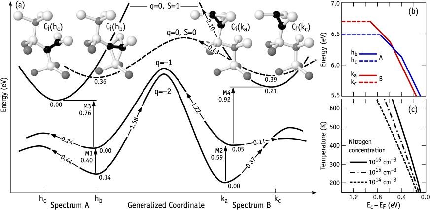
Figure 1(b) shows the formation energy of C in -SiC as a function of the Fermi level with respect to the conduction band bottom, . It was calculated by assuming a C-rich crystal with the carbon chemical potential obtained from bulk diamond. For the sake of clarity, line styles are connected to specific geometries (see legend) and the range of values span the upper half of the gap only. Besides a charge state-dependent structure, C finds its most favorable sublattice site depending on the location of the Fermi level. In n-type material (without external bias), the most stable state is , whereas if the Fermi level is brought toward midgap (reverse bias conditions), the ground state is . This behavior closely follows that of the center and its spectra A and B, hereafter assigned to and , respectively.
Although the charge of defects is not directly accessible by capacitance measurements, the lack of a Poole-Frenkel effect for the M emissions indicates that they involve acceptor transitions (Nielsen et al., 2005). Directly measured capture cross-sections of the shallower M1 and M2 traps were about , suggesting transitions. The cross-section of M3 was two orders of magnitude larger, consistent with M1 and M3 being two consecutive electron emissions from the same structure (spectrum A). M2 plus a conjectured (undetected) M4 peak would account for the analogous transitions in spectrum B. Hence, the type and number of transitions conform with the assignment of C to M.
The center anneals out in the temperature range 580-640 K according to first order kinetics at a rate of , suggesting a dissociation mechanism or capture by an abundant and close trap (Nielsen et al., 2005). Figure 1(c) gives the calculated Fermi energy in -SiC as a function of temperature for three different nitrogen doping levels. The horizontal axis matches that of the formation energy diagram in Fig. 1(b). Considering the doping concentration of the samples in Ref. (Nielsen et al., 2005), we conclude that the annealing temperature range coincides with the Fermi level window for which C is in the single negative charge state. From NEB calculations we find that the barriers for migration of along crystalline basal and axial directions are 1.8 and 2.2 eV, respectively, the latter being the highest of two jumps between consecutive sublattice sites, and close to the measured activation energy for the annealing of the center (Nielsen et al., 2005).
Let us now compare the charge state transition levels of C with those of the center. The calculated figures are shown in Fig. 1(a). The energies next to the vertical arrows (in eV) stand for trap depths with respect to the conduction band bottom. Accordingly, has second and first acceptor transitions calculated at eV and eV, very close to the measured transitions of spectrum A, namely M1 ( eV) and M3 ( eV). Analogously, for we find second and first acceptor transitions at eV and eV. The former agrees well with M2 ( eV) from spectrum B, while the latter anticipates the location of M4. The calculated levels neglect any temperature effects. They differ from the measured activation energies by a capture barrier and an entropy contribution, usually eV. Hence, the agreement obtained is considered very good.
Besides the above, the calculated conversion barriers further confirm that the center in -SiC is a carbon interstitial. Like the carbon vacancy (Bathen et al., 2019b), in order to travel between two equivalent lattice sites along the main crystalline axis, C must perform two types of jumps between consecutive sublattice configurations. The jump with lower barrier is represented in Fig. 1(a) and separates from structures. Calculated barrier heights of 1.58 and 1.22 eV were obtained for forward and backward jumps and , respectively. Both mechanisms are exothermal, and the barriers are rather close to the and conversion activation energies of 1.4 and 0.9 eV, measured without and with bias, respectively (Martin et al., 2004).
A decisive piece of evidence in the identification of the center would be a direct observation of the M4 transition accompanied by M2. Figure 2(a) shows DLTS spectra of a -SiC n-type sample implanted with 2 MeV He ions, measured after annealing at 340 K under reverse bias (spectrum A) and 450 K without bias (spectrum B). The latter is dominated by the Z1/2 peak (carbon vacancy) (Hemmingsson et al., 1998; Son et al., 2012), with relatively smaller contributions from S1/S2 (silicon vacancy) (David et al., 2004; Bathen et al., 2019a), and a less understood broad feature known as EH4, recently connected to a superposition of different alignments of anisotropic silicon vacancy structures commonly referred to as carbon-antisite-vacancy pairs (Karsthof et al., 2020).
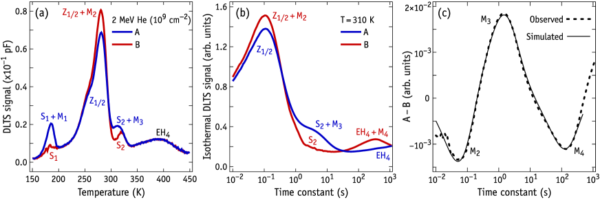
It is only when we compare spectrum B with A that the presence of the bistable center becomes evident. The prominent peak at about 280 K in spectrum B is actually a superposition of Z1/2 with M2, the latter being converted to M1 and M3 in spectrum A (overlapping S1 and S2, respectively). As in Ref. (Nielsen et al., 2005) we find that above room temperature spectra A and B become identical as a result of the transformation. This means that we do not have access to center related transitions deeper than M3 (as it is expected for the location of M4) by means of conventional DLTS.
Figure 2(b) depicts two isothermal DLTS spectra acquired sequentially at K. Spectrum B was acquired first, after pre-annealing the sample at 450 K with no bias applied. During the 20-min recording time at K, a large fraction of centers was converted from configuration B to A. This could be confirmed from the loss of intensity of M2 during subsequent identical measurements. Spectrum A was then recorded after warming up the sample at K under reverse bias ( V ) in order to reset all centers to the A form. The isothermal signals have contributions from three groups of transients: A fast group with time constant s (Z1/2 and M2), an intermediate group with decay time of a few seconds (S2 and M3), and a slow group in the range s (EH4 and a new peak labeled M4). The M4 peak is clearly shown in the differential spectrum of Fig. 2(c). It has the same behavior of M2 on annealing/biasing, and corresponds to a trap concentration identical to that of M1, M2, and M3 ().
From a fit of a -corrected Arrhenius function to the M4 data, we obtain an activation energy for electron emission of eV and an extrapolated capture cross-section which is coherent with a first acceptor transition. Although we could not directly measure the capture cross-section of M4, the agreement with the calculated transition energy of 0.92 eV is striking. Also notable is the agreement shown in Fig. 2(c) between the isothermal data (dotted line) and its theoretical counterpart (solid line) (Tokuda et al., 1979), obtained via non-linear fitting constrained by the measured emission rates of M2, M3 and M4.
Unfortunately, the measurements cannot discern whether M4 is an evidence of (i) followed by or (ii) immediately followed by . The second and first steps of (i) and (ii), respectively, are necessary to explain the gradual conversion of B into A during the isothermal transients. The calculations account for in (i) if we consider the spin-flipping transition shown as a dashed line in the CCD. On the other hand, the first step of route (ii) has a measured activation energy of 0.9 eV, very close to the M4 emission energy, and this could reflect the rate-limiting process toward . Regarding the C model, although being consistent with both alternatives, this issue certainly calls for further clarification.
Another aspect that deserves a closer look, concerns the annealing mechanism of the M center. The observed first order kinetics suggests an annealing rate that depends on its own concentration only. A possible explanation stems from the indication that C defects are most likely negatively charged during annealing, thus being Coulomb-attracted by abundant nitrogen donors. The products of such reaction could be the EB centers reported by Beyer et al. (Beyer et al., 2011).
The list of alternative defects, other than C, that could be related to the center is not long. A Si displacement is unlikely, given that M was observed in material irradiated with electrons whose energy was below the necessary displacement threshold (Beyer et al., 2011). Further, we know that the Si self-interstitial is not an acceptor and has levels considerably deeper than those of M (Coutinho, 2021).
A stronger contender is a carbon Frenkel pair. Carbon vacancies and self-interstitials have electron traps deeper than eV. In n-type material they are both negatively charged, and Coulomb interactions between pairs with varying distances should lead to a strong dispersion of their respective trap depths. This effect is observed in DLTS spectra of as irradiated samples, but does not conform with the relatively clean M peaks, which are only visible after a gentle () annealing (Doyle et al., 1998; David et al., 2004). We investigated the stability of close Frenkel pairs and found a family of markedly low-energy structures. Their formation energy is in the range 5.5-6.5 eV but the annihilation barrier is about 0.1-0.2 eV and therefore could not survive even at room temperature.
Based on first-principles calculations and junction spectroscopy, we provide substantial and credible arguments that allow us to conclude that the center in -SiC is a carbon self-interstitial. The observation of a new peak, labeled M4 and possibly connected to a previously anticipated acceptor transition, provides an important piece of evidence in the connection between M and the interstitial. The model developed is summarized in Fig 1(a) in the form of a CCD. It incorporates the observed features of M, including charge states, bistability, annealing, reconfiguration kinetics and electronic transition levels. The center peaks are either “hidden” by the prominent Z1/2 signal (carbon vacancy) or by S1/2 (silicon vacancy) and EH1/3 (unidentified). While this may explain the difficulty in the identification of C in n-type -SiC, it certainly has undermined the interpretation of defect evolution by means of DLTS, in particular during annealing. The identification of the center in -SiC as the C defect will contribute to a better understanding of defect-related processes, ranging from self-diffusion to the activation and migration of dopants and impurities introduced by ion-implantation.
Acknowledgments
This work was supported by the NATO SPS Programme through Project G5674. J.C. thanks the FCT in Portugal for support through Projects UIDB/50025/2020, UIDP/50025/2020, and CPCA/A0/7277/2020 (Advanced Computing Project using the Oblivion supercomputer). J.D.G. acknowledges the support of I3N through Grant BPD-11(5017/2018). T.O. thanks Dr. Hidekazu Tsuchida and Dr. Norihiro Hoshino at CRIEPI for growing the -SiC epitaxial layers. Z.P. acknowledges the financial support of the Australian Government to the CAS of ANSTO through the NCRIS.
References
- Kimoto and Cooper (2014) T. Kimoto and J. A. Cooper, Fundamentals of silicon carbide technology: growth, characterization, devices and applications (John Wiley & Sons, Singapore, 2014).
- She et al. (2017) X. She, A. Q. Huang, O. Lucia, and B. Ozpineci, IEEE Transactions on Industrial Electronics 64, 8193 (2017).
- Weber et al. (2010) J. R. Weber, W. F. Koehl, J. B. Varley, A. Janotti, B. B. Buckley, C. G. V. de Walle, and D. D. Awschalom, Proceedings of the National Academy of Sciences 107, 8513 (2010).
- Koehl et al. (2011) W. F. Koehl, B. B. Buckley, F. J. Heremans, G. Calusine, and D. D. Awschalom, Nature 479, 84 (2011).
- Ivády et al. (2019) V. Ivády, J. Davidsson, N. Delegan, A. L. Falk, P. V. Klimov, S. J. Whiteley, S. O. Hruszkewycz, M. V. Holt, F. J. Heremans, N. T. Son, D. D. Awschalom, I. A. Abrikosov, and A. Gali, Nature Communications 10, 5607 (2019).
- Castelletto and Boretti (2020) S. Castelletto and A. Boretti, Journal of Physics: Photonics 2, 022001 (2020).
- Son et al. (2012) N. T. Son, X. T. Trinh, L. S. Løvlie, B. G. Svensson, K. Kawahara, J. Suda, T. Kimoto, T. Umeda, J. Isoya, T. Makino, T. Ohshima, and E. Janzén, Physical Review Letters 109, 187603 (2012).
- Trinh et al. (2013) X. T. Trinh, K. Szász, T. Hornos, K. Kawahara, J. Suda, T. Kimoto, A. Gali, E. Janzén, and N. T. Son, Physical Review B 88, 235209 (2013).
- Capan et al. (2018) I. Capan, T. Brodar, Z. Pastuović, R. Siegele, T. Ohshima, S.-i. Sato, T. Makino, L. Snoj, V. Radulović, J. Coutinho, V. J. B. Torres, and K. Demmouche, Journal of Applied Physics 123, 161597 (2018).
- Son et al. (2019) N. T. Son, P. Stenberg, V. Jokubavicius, T. Ohshima, J. U. Hassan, and I. G. Ivanov, Journal of Physics: Condensed Matter 31, 195501 (2019).
- Defo et al. (2018) R. K. Defo, X. Zhang, D. Bracher, G. Kim, E. Hu, and E. Kaxiras, Physical Review B 98, 104103 (2018).
- Udvarhelyi et al. (2020) P. Udvarhelyi, G. Thiering, N. Morioka, C. Babin, F. Kaiser, D. Lukin, T. Ohshima, J. Ul-Hassan, N. T. Son, J. Vučković, J. Wrachtrup, and A. Gali, Physical Review Applied 13, 054017 (2020).
- Bathen et al. (2019a) M. E. Bathen, A. Galeckas, J. Müting, H. M. Ayedh, U. Grossner, J. Coutinho, Y. K. Frodason, and L. Vines, npj Quantum Information 5, 111 (2019a).
- Hiyoshi and Kimoto (2009) T. Hiyoshi and T. Kimoto, Applied Physics Express 2, 041101 (2009).
- Løvlie and Svensson (2011) L. S. Løvlie and B. G. Svensson, Applied Physics Letters 98, 052108 (2011).
- Hemmingsson et al. (1997) C. Hemmingsson, N. T. Son, O. Kordina, J. P. Bergman, E. Janzén, J. L. Lindström, S. Savage, and N. Nordell, Journal of Applied Physics 81, 6155 (1997).
- Alfieri and Mihaila (2020) G. Alfieri and A. Mihaila, Journal of Physics: Condensed Matter 32, 465703 (2020).
- Martin et al. (2004) D. M. Martin, H. Kortegaard Nielsen, P. Lévêque, A. Hallén, G. Alfieri, and B. G. Svensson, Applied Physics Letters 84, 1704 (2004).
- Nielsen et al. (2005) H. K. Nielsen, A. Hallén, and B. G. Svensson, Physical Review B 72, 085208 (2005).
- Beyer et al. (2011) F. C. Beyer, C. Hemmingsson, H. Pedersen, A. Henry, E. Janzén, J. Isoya, N. Morishita, and T. Ohshima, Journal of Applied Physics 109, 103703 (2011).
- Bockstedte et al. (2003) M. Bockstedte, A. Mattausch, and O. Pankratov, Physical Review B 68, 205201 (2003).
- Gali et al. (2003) A. Gali, P. Deák, P. Ordejón, N. T. Son, E. Janzén, and W. J. Choyke, Physical Review B 68, 125201 (2003).
- Kobayashi et al. (2019) T. Kobayashi, K. Harada, Y. Kumagai, F. Oba, and Y. ichiro Matsushita, Journal of Applied Physics 125, 125701 (2019).
- Itoh et al. (1997) H. Itoh, A. Kawasuso, T. Ohshima, M. Yoshikawa, I. Nashiyama, S. Tanigawa, S. Misawa, H. Okumura, and S. Yoshida, physica status solidi (a) 162, 173 (1997).
- Son et al. (2001) N. T. Son, P. Hai, and E. Janzén, Materials Science Forum 353-356, 499 (2001).
- Petrenko et al. (2002) T. T. Petrenko, T. L. Petrenko, and V. Y. Bratus, Journal of Physics: Condensed Matter 14, 12433 (2002).
- Gerstmann et al. (2010) U. Gerstmann, A. P. Seitsonen, D. Ceresoli, F. Mauri, H. J. von Bardeleben, J. L. Cantin, and J. G. Lopez, Physical Review B 81, 195208 (2010).
- Lefèvre et al. (2009) J. Lefèvre, J.-M. Costantini, S. Esnouf, and G. Petite, Journal of Applied Physics 105, 023520 (2009).
- Hemmingsson et al. (1998) C. G. Hemmingsson, N. T. Son, A. Ellison, J. Zhang, and E. Janzén, Physical Review B 58, R10119 (1998).
- David et al. (2004) M. L. David, G. Alfieri, E. M. Monakhov, A. Hallén, C. Blanchard, B. G. Svensson, and J. F. Barbot, Journal of Applied Physics 95, 4728 (2004).
- Blöchl (1994) P. E. Blöchl, Physical Review B 50, 17953 (1994).
- Kresse and Furthmüller (1996a) G. Kresse and J. Furthmüller, Computational Materials Science 6, 15 (1996a).
- Kresse and Furthmüller (1996b) G. Kresse and J. Furthmüller, Physical Review B 54, 11169 (1996b).
- Heyd et al. (2003) J. Heyd, G. E. Scuseria, and M. Ernzerhof, The Journal of Chemical Physics 118, 8207 (2003).
- Perdew et al. (1996) J. P. Perdew, K. Burke, and M. Ernzerhof, Physical Review Letters 77, 3865 (1996).
- Henkelman et al. (2000) G. Henkelman, B. P. Uberuaga, and H. Jónsson, The Journal of Chemical Physics 113, 9901 (2000).
- Freysoldt et al. (2014) C. Freysoldt, B. Grabowski, T. Hickel, J. Neugebauer, G. Kresse, A. Janotti, and C. G. V. de Walle, Reviews of Modern Physics 86, 253 (2014).
- Freysoldt et al. (2009) C. Freysoldt, J. Neugebauer, and C. G. Van de Walle, Physical Review Letters 102, 016402 (2009).
- Bathen et al. (2019b) M. E. Bathen, J. Coutinho, H. M. Ayedh, J. U. Hassan, I. Farkas, S. Öberg, Y. K. Frodason, B. G. Svensson, and L. Vines, Physical Review B 100, 014103 (2019b).
- Coutinho (2021) J. Coutinho, Crystals 11, 167 (2021).
- Tokuda et al. (1979) Y. Tokuda, N. Shimizu, and A. Usami, Japanese Journal of Applied Physics 18, 309 (1979).
- Tokuda (2006) Y. Tokuda, Journal of Applied Physics 100, 023704 (2006).
- Hunt et al. (2000) D. C. Hunt, D. J. Twitchen, M. E. Newton, J. M. Baker, T. R. Anthony, W. F. Banholzer, and S. S. Vagarali, Physical Review B 61, 3863 (2000).
- Karsthof et al. (2020) R. Karsthof, M. E. Bathen, A. Galeckas, and L. Vines, Physical Review B 102, 184111 (2020).
- Doyle et al. (1998) J. P. Doyle, M. K. Linnarsson, P. Pellegrino, N. Keskitalo, B. G. Svensson, A. Schöner, N. Nordell, and J. L. Lindström, Journal of Applied Physics 84, 1354 (1998).