Identifying the mechanism of single-domain single-layer MoS2 growth on Au(111)
Abstract
The nucleation and growth of single-layer molybdenum disulfide single domain islands is investigated by in situ low-energy electron microscopy. We study the growth of micron-sized flakes and the correlated flattening process of the gold surface for three different elevated temperatures. Furthermore, the influence of surface step edges on the molybdenum disulfide growth process is revealed. We show that both island and underlying terrace grow simultaneously by pushing the surface step in the expansion process. Our findings point to an optimized growth procedure allowing for step-free single-domain single-layer islands of several micrometers in size, which is likely transferable to other transition metal dichalcogenides.
Keywords: LEEM, low-energy electron microscope, molybdenumdisulfide, monolayer, 2D material, epitaxial growth, Au(111)
1 Introduction
Since the first studies illustrating the extraordinary electronic properties of graphene [1], similar characteristics were predicted for other 2D materials, such as single-layer (SL) transition metal dichalcogenides (TMDs)[2]. A promising example in terms of applications and probably the most prototypical one is SL molybdenum disulfide (MoS2) as the band structure has been predicted to exhibit a direct band gap [3]. Indeed, this transition from an indirect semiconductor in its bulk form to a direct semiconductor as a 2D SL has also been demonstrated experimentally [4, 5], resulting in attractive optoelectronic properties[6] and an interesting valley/spin valley structure[7, 8]. First functioning MoS2 transistor devices have been reported[9] as well as optoelectronic devices[10]. Furthermore, from a chemical point of view, MoS2 has since long been known to be an excellent catalyst for sulfurization and desulfurization processes [11, 12, 13], rendering MoS2 a versatile material for various applications in heterogeneous catalysis and chemical sensing.
Most studies have used mechanical exfoliation to produce SL MoS2 [4, 5, 8, 7, 9, 10] whereas the research employing more industrially suitable growth methods such as chemical vapor deposition (CVD)[14, 15, 16, 17, 18] are gaining increasing interest due to its scalability for large-scale fabrication. Even though remarkable first results have been reported using CVD, a deeper understanding of the growth mechanism would further improve the growth control and hence the structural quality of the films, i.e., its single-crystalline nature. To achieve this ambitious goal, key ingredients are the suppression of defects as well as the manipulation of the island expansion to ensure the desired quality and size of the SL MoS2. This knowledge is usually best obtained in dedicated epitaxial growth studies using in situ experimental methodology for a model system, here MoS2 on Au(111).
So far, epitaxial growth studies of this MoS2/Au(111) model system have focused on investigating the electronic structure and catalytic properties, mostly addressing individual SL nanoclusters and islands found at low coverage[19, 20] as well as monolayer-like coverages of many SL MoS2 islands [21, 22, 23]. Whereas bulk MoS2 may occur in various polymorphs, SL MoS2 has been found to exist in its thermodynamically most stable form, the three-fold symmetric 1H-structure, where the islands are terminated by S-edges and Mo-edges at high and low values of the sulfur chemical potential, respectively[24]. The six-fold symmetry of the first layer of the Au substrate facilitates the growth of MoS2 mirror domains, i. e., of islands azimuthally rotated by 60∘ [20, 25]. Recently, Bana et al[26] presented a growth study where they were able to suppress one of the mirror domains and get large single-domain SL MoS2, whereas a study by Bignardi et al[27] reported similar results of mostly single-domain SL WS2, demonstrating the feasibility of modifying the epitaxial growth process by a suitable choice of parameters. This single-domain coverage enabled revealing the spin structure of WS2 by Eickholt et al[28], suggesting that a precise control of the growth process is highly desirable for large-scale integration of SL TMD and the exploitation of their superior materials properties in applications. The origin of the observed asymmetry, however, remained ambiguous, leaving a knowledge gap in our understanding of the growth process of MoS2, and especially the transition from nanoclusters to large single-domain SL.
Here, we present the first in situ study in which we finally unravel the mechanism that is fostering the growth of a single orientation of MoS2 islands on the Au surface. Following the nucleation and growth process in real-time allows us, for the first time, to reveal and explicitly focus on the dynamic interplay between the substrate and the occurring islands leading to this distinct domain distribution. Furthermore, our results strongly indicate that the proposed mechanism very likely is a key feature promoting single-domain growth of TMDs on Au(111).
2 Experimental
Au(111) single crystal substrates were cleaned by Ar+ ion sputtering at 0.5 kV for 1 h followed by thermal annealing at 700 ∘C for 30 min. This procedure was repeated several times before the cleaning process was finalized by annealing at 950 ∘C for 5 min. The deposition experiments started with the surface showing a well defined herringbone reconstruction in low-energy electron diffraction (LEED) as reported by Barth et al. [29] for a clean Au(111) surface.
The in-situ characterization of MoS2 growth on Au(111) was performed using a commercial ELMITEC LEEM III microscope under ultra-high vacuum (UHV) conditions with a base pressure of 110-10 torr. Low-energy electron microscopy (LEEM) allows to directly monitor the sample surface at video rate with a spatial resolution of about or even below 10 nm. Being based on diffraction, LEEM enables recording either real space (imaging mode) or reciprocal space images (diffraction mode).
LEEM also allows for choosing among different contrast modes. A contrast aperture placed into the back focal plane of the objective lens (where the diffraction pattern is generated) can be used to select an imaging beam and suppress the others. The (00) specular beam is used for bright-field imaging, which is applied here for observing MoS2 growth in time-resolved imaging sequences. In addition, by selecting a particular non-specular beam in so-called dark-field imaging, the resulting diffraction contrast can be used to discriminate between different phases (here rotational domains of MoS2/Au(111)) since only areas on the sample surface will appear bright in the image if they contribute to the intensity of the particular diffracted beam in reciprocal space.
Inserting an illumination aperture into the incident beam, the illuminated area of the sample can be constrained down to 250 nm, facilitating the recording of diffraction patterns of local origin. This diffraction mode is called µLEED. Micro-spectroscopy and spectro-microscopy can be performed with LEEM by spatially resolved recording of the electron reflectivity as a function of electron energy. Due to its analogy to the well-established method of I(V)-LEED[30], this mode is called I(V)-LEEM. The corresponding experimental procedure is based on measuring the electron reflectivity in bright-field LEEM imaging mode for a range of electron energies, typically from the vacuum level up to a few tens of electronvolts. The corresponding energy-dependent reflectivity curve can be extracted with pixel resolution, yielding a lateral spatial resolution near or even below 10 nm in favorable circumstances. The shape of the curve is derived from the band structure of the unoccupied states of the sample near-surface region, resulting in a material-specific and chemically sensitive structural fingerprint [31]. Further information on LEEM methodology can be found in the literature[32, 33].
For MoS2 growth, sulfur was supplied from a dimethyldisulfide (DMDS) vapor source backfilling the UHV chamber to 110-6 torr when dosing. DMDS is a suitable and safe sulfiding agent since it was previously shown to lead to facile formation of single-layer MoS2 on Au(111) in the temperature range of interest here [34]. The DMDS vapor background pressure was upheld during the entire growth process reported here. Molybdenum (purity 99.95%) was evaporated from a home-built electron beam evaporator similar to existing commercial designs. MoS2 growth was performed in an experiment series employing three different substrate temperatures, i. e., 650 ∘C, 700 ∘C, and 750 ∘C. To ensure sufficiently stable imaging conditions, the sample was heated to the desired temperature by electron beam heating 10 min prior to the growth process. Thereafter, molybdenum was deposited at a very low rate of 0.108ML/h onto the sulfur-terminated sample surface. The growth rate has been determined from the overall coverage of MoS2 islands on the Au(111) surface extracted from large-scale LEEM survey images and set into relation to the total evaporation time of Mo.
3 Results and Discussion
All deposition experiments started with exposing the Au(111) surface at growth temperature to DMDS (no Mo flux) for 10 min. For the lower growth temperatures of 650 ∘C and 700 ∘C, this procedure resulted in lifting the herringbone reconstruction of the clean Au(111) surface and forming a (11) LEED pattern. This is attributed to sulfur deposition on the Au(111) surface [35]. For the highest growth temperature of 750 ∘C, however, the herringbone reconstruction was visible in diffraction mode after the deposition, pointing towards a desorption of sulfur atoms at this temperature.
MoS2 nucleation is initiated by reactive deposition of Mo on the sample surface in the DMDS background pressure. Throughout the deposition, the sample is held at the desired growth temperature, i. e., 650 ∘C, 700 ∘C or 750 ∘C. After deposition of the first few mML (0.001 monolayers), island nucleation was observed in the LEEM image, reflecting that the critical nucleus size had been reached under these conditions. In all observed cases, the nucleation centers of the islands are found on the Au terraces; no tendency for preferential nucleation at steps was observed.
In fig. 1a) a newly nucleated MoS2 island (growth temperature: 650 ∘C) is shown. The corresponding µLEED diffraction pattern (fig. 1b)) of a single MoS2 island has been recorded from a MoS2 covered area of 1 µm in diameter after the growth. It is clearly dominated by the moiré structure of MoS2/Au(111), which will be analyzed below. The diffraction pattern is threefold symmetric, as expected for a single domain of SL MoS2(0001). Furthermore, spectromicroscopy, as shown in fig. 1c), clearly confirms the island to consist of a single layer of MoS2.
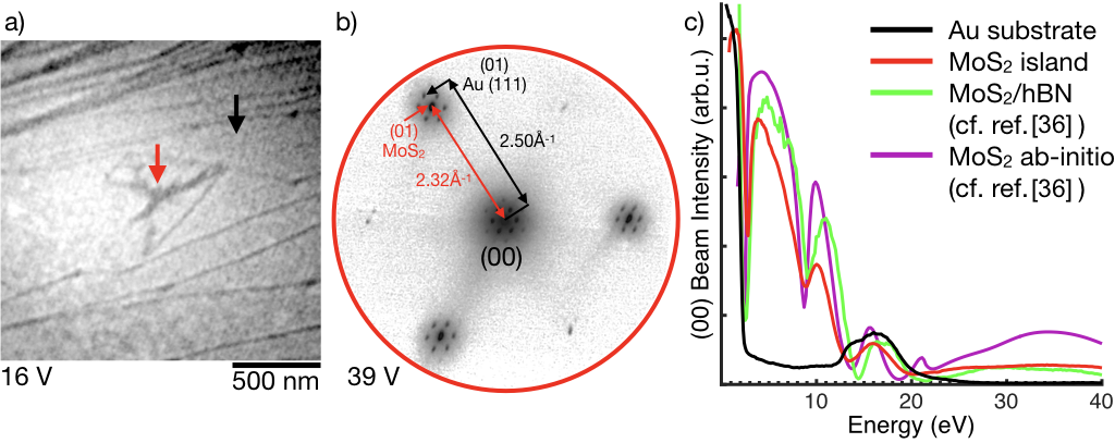
From the exact position of the moiré spots relative to the three integer reflections, the lattice mismatch between MoS2 and Au(111) and thus the MoS2 lattice parameter is determined to 3.14 Å, in excellent agreement with the in-plane lattice constant of the bulk crystal [37]. Together with the threefold symmetry of the diffraction pattern, our findings suggest the formation of unstrained single-layer islands of 1H-MoS2 on Au(111), consistent with previous reports [22, 23].
Generally, the crystalline and electronic structure of any material determine the specular electron reflectivity depending on kinetic electron energy, the so-called curve, allowing to locally identify a material and its structure by comparing the recorded curves to calculated spectra or experimental reference data [31]. Here, after the growth we have identified only two distinct types of curves representing the substrate and the islands as shown in fig. 1c). The fingerprint of the island (fig. 1c)) is in good agreement with the reference curve of exfoliated single-layer MoS2 on hBN presented by DeJong et al[36] and clearly differs from the corresponding bi- and trilayer curves (not shown). Strikingly, an even better match is observed when comparing our curve of MoS2/Au(111) to the calculated spectra for SL MoS2 as presented in [36] based on ab initio scattering theory [38]. This finding implies that the orbitals facilitating the bonding to the substrate do neither significantly affect the bandstructure above the vacuum level nor do they facilitate an efficient coupling to the incident plane wave in the scattering process. It is, however, noted that angle-resolved photoemission (ARPES) and density functional theory calculations have shown that substrate bonding and modification of the out-of-plane orbitals associated with the -point is relevant for MoS2 bonded to Au(111) [20, 21]. Taken together, these observations suggest that the bonding orbitals at the interface are indeed too strongly localized to effectively couple to the incident plane wave, rendering them invisible to microspectroscopy.
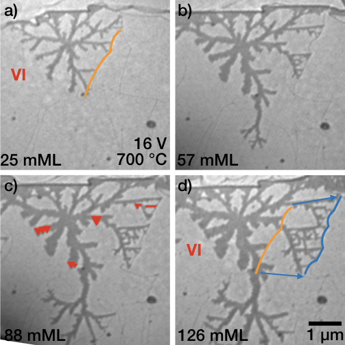
At a later stage of the deposition at all selected temperatures, the islands growth proceeds by ramification as depicted in the LEEM time-lapse sequence in fig. 2 for growth of MoS2 at 700 ∘C. At this electron energy (16 eV) the bare Au substrate appears bright and the MoS2 islands are dark. Furthermore, the step edges of the Au(111) surface appear dark in the LEEM images due to phase contrast.
In the growth regime of strong excess sulfur supply as applied here, literature suggests that MoS2 islands are fully sulfided and that preferentially single-layer MoS2 islands with a triangular morphology are formed.[24, 20, 25]. The predominant triangular morphology results from a higher stability of one type of zig-zag edge termination of a single layer MoS2 sheet, the so-called (100) Mo-edge, as compared to the other, i. e., the (010) S-edge. Most isolated islands therefore assume either a perfect triangular shape or a shape of a slightly truncated triangle with long Mo-edges and short S-edges. This is also the case for the MoS2 structure in fig. 2, where the expanding island keeps its three-fold symmetry as it grows in substructures of the typical triangular shape out of the extending branches (see red triangles in fig. 2c)). As pointed out by Grønborg et al[23], there are two rotational domains of epitaxially grown MoS2 on Au(111) due to the six-fold symmetry of the first substrate layer and the three-fold symmetry of MoS2. In fig. 2, all the triangular substructures point in the same direction, reflecting that the ramified island consists of a coherent single rotational domain of MoS2.
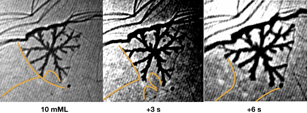
From the analysis of an expanding growth front, it is also observed that whenever the island reaches a substrate step edge, the island either stops expanding in this direction, or makes the step edge move itself, thereby expanding the Au terrace beneath the island. The latter case is illustrated in fig. 2. At growth stage a) (i.e. 25 mML) a downward step bunch on Au(111) is present at the position identified by an orange line. During growth the step bunch moves in front of the growing island, as seen at growth stages b) and c) (i.e. 57 and 88 mML). This process is ongoing over the entire growth sequence analyzed here. The progression of the step bunch from 25 to 126 mML is indicated by the orange and blue lines as well as the arrows in fig. 2(d).
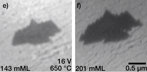
Interestingly, such step movement (referred to as step-pushing in the following) can only be observed for growth of the MoS2 majority domain. For the MoS2 minority domain, no indication of step-pushing is found as exemplarily shown for an island during growth at 650 ∘C (figs. 3 a) and b)). Distinct from the strongly ramified shape of the majority islands, this minority island exhibits a dense, compact triangular shape without any visible branches. Obviously, the inability to push the step edge seems to limit the growth to the existing terrace on the Au surface only, in stark contrast to the previous finding of continuing growth of islands of the majority domain.
To explain the observation of majority-domain ramification growth by Au step-edge displacement in specific directions only, we note that a single domain orientation of MoS2 implies two possible orientations of the triangular MoS2 island relative to a [111]-oriented Au step edge. These two scenarios are schematically shown in fig. 4.
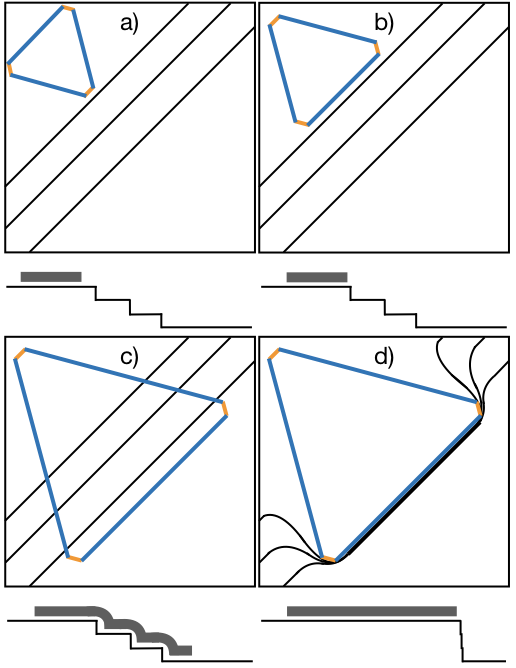
In scenario a), the () S-edge (indicated as orange lines in fig. 4) is parallel to the Au step edge, so the apex of the triangular island contacts the step edge upon growth. Oppositely, in scenario b), the () a long side of the MoS22 island touches the step edge forming a long contact line with it. As mentioned above, this side ist the Mo-edge of the MoS22 structure (indicated as blue lines in fig. 4).
Our LEEM observations exclusively find a termination of growth if the apex of the island collides wit a step. , whereas the approach of a long side of an island, i.e. its Mo-edge terminated side) initiates two scenarios of progressive growth in two different ways, c.f. scenario overgrowth of the step or step pushing as displayed in fig. 4 c) and d).
Scenario c) shows the MoS2 island growing over several step edges without any movement of the step edges themselves. In this scenraio the island is bent similar to a carpet to cover the height differences of the underlying substrate. In scenario d) the movement of the step edge and consequently the growth of the terrace (step pushing) allows the island to expand further on the same terrace without any bending.
Step restructuring driven by the formation of Lander islands has already been reported for the Cu(110) [39]. For this system, the formation of Cu(110) nanostructures at step edges has been found to be energetically favored by the adsorption of a single Lander molecule fitting perectly onto the metal nanostructure. For the Cu(111) surface a process of step bunching has been found upon exfoliation and mild annealing of single layer graphene onto a foil of Cu(111) [40]. The argument for massive step rearrangement found here, is an energy gain for the adsorbed graphene by the reduction of graphene bending across step edges. A similar step-restructuring argument can be claimed here due a high mobility of surface Au atoms induced by the relatively high growth temperatures in our experiments. Here, however, step rearrangement occurs during growth as in the case of metal nanostructure formation on C(110). Applying this argument, the following factors influencing the growth mechanism can be derived. Firstly, a crossing of a step edge by the. expanding the MoS22 islands would lead to a sequential downward and upward bending of the MoS2 island (see fig. 4, lower part) the resulting stress in the island itself makes this growth step energetically unfavorable. This conclusion is supported by our extensive growth observations which did not reveal any crossing of a step edge by a MoS2 island. Secondly, the area of contact to the step edge determines whether or not the step edge will move. Again from an energetically point of view the diffusing Au atoms already on the step edge are more likely to remain longer at a step edge than a terrace site. Considering the additional influence of a near MoS2 island which has reached the end of the terrace and would have to bend itself to reach the next terrace this is expected to be even more favorable. If the islands reaches to step with its Mo-egde, as sketched in fig. 4 scenario d), the terrace can expand parallel to the step edge keeping the length of the step edge equally long. Therefore, the surface energy is not or only slightly influenced by the shape of the moving step edge. If, however, the islands reaches to step with its S-edge, i.e. its triangular tip, a terrace expansion would result in a triangular step line of an uncommon shape and additional step length. Consequently, this results in an energy burden and a higher formation energy.
The question if step pushing occurs in upward or downward direction of the substrate can be ansewered by LEEM using routines established by Bauer [41] and Kennedy et al[42, 43]. Tuning the objective lens focus accoridingly, we find step pushing occuring on downward steps exclusively for growth temperatures of 700 ∘C and lower.
For our highest growth temperature (i.e. 750 ∘C), however, also a very slow movement of an upward step edge fduring growth of a MoS2 island could be observed. The fact that this only was observed at 750 ∘C reflects that the Au atoms are thermally highly activated at this temperature and detach from the step edge. This growth scheme, however, is the result of a delicate balance between island growth speed and step edge mobility. Additional experiments with an increased growth rate (2.36 ML/h) show that step pushing is suppressed by the supply of additional material forcing the MoS2 island to grow over the step edges before the terrace has time to expand.
In oder to identify the dring force for island ramnification, a close inspection of the area in fig. 5 marked as VI is revealing. Up to a deposit of 10mML, the island has expanded by ramnification. The underlying growth scheme is step pushing as discussed above. At this point, the situation changes by the collision of two steps of identical height but opposite sign, i.e. step annihilation. This process occures at a much faster time scale than island expansion. The collision of the steps is highlighted by orange lines in fig. 5. Upon collsion, the remaining steps withdraw and leave the island branches ending on some inner part of a (newly formed) wide terrace. Immediately, the growth scheme for these branches switches from ramnification to broadening while the branches on the other island side still in contact to a step and further progress by ramnification. This concludes, that contact to a step edge is necessary for the ramification growth. Without step contact, the island is expanding two-dimensionally with no favored direction in the expected triangular shape. For a substrate with a sufficiently high step density, the domination growth scheme is ramification growth. This favors the growth of islands with the proper alignment towards the step edges and finally results in a high coverage for this type of islands.
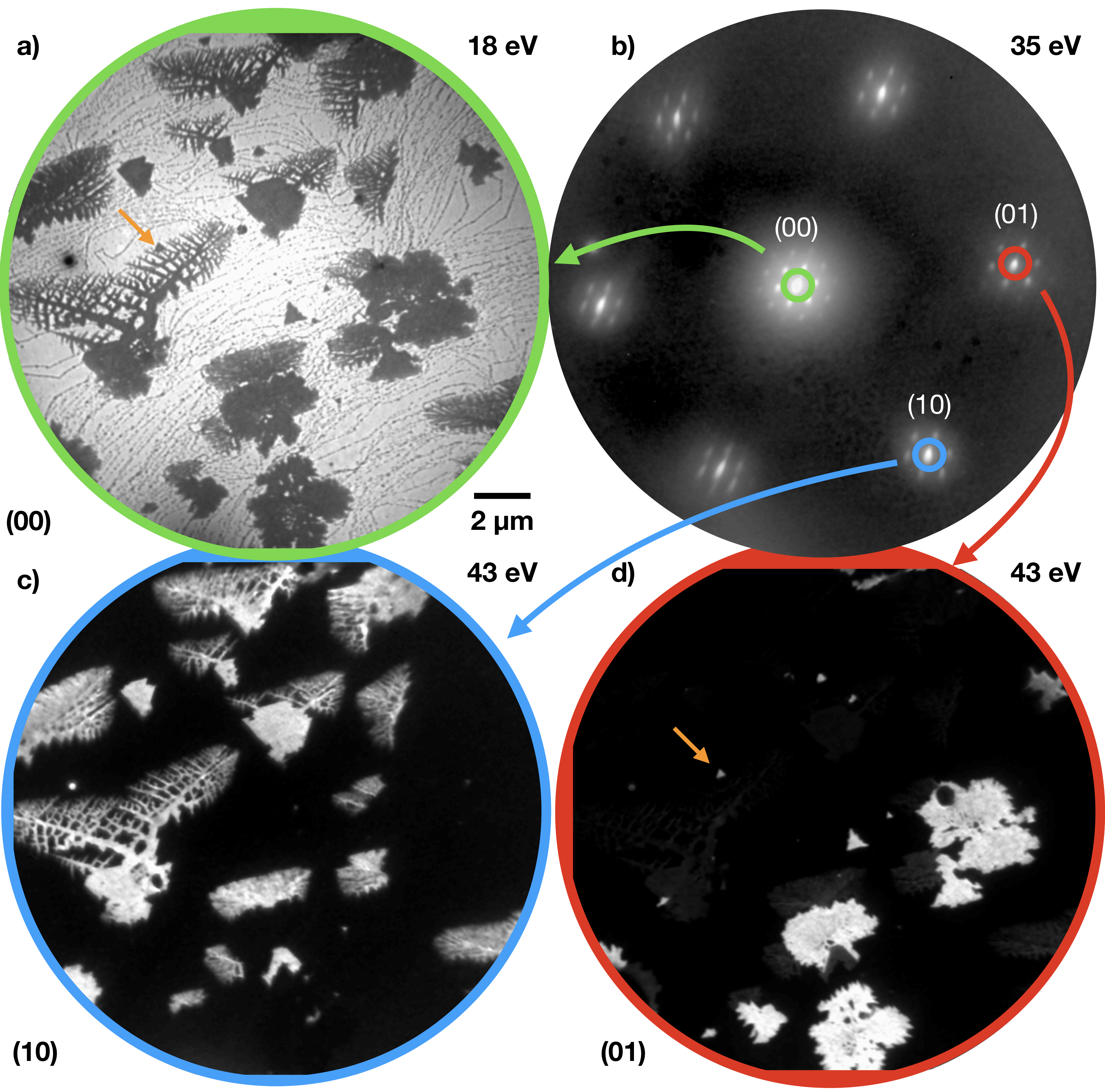
Depending on the miscut and its orientation, this mechanism leads to favoring growth of one of the to existing MoS2 domains over the other. The distribution of the two MoS2 domains can be measured in LEEM using dark field imaging as shown in fig. 6. While the two domains are indistinguishable in bright-field LEEM, the contribution of the two domains to the higher order diffraction spots varies differently with electron energy. At 43 e, the difference between the two is large, resulting in strong contrast between the MoS2 domains. Employing the (01) beam only one of the domains appears bright in the image of fig. 6 c) , while imaging with the (10) beam provides an image of the other domain in fig. 6 d) with no contribution of the first. The bright field image of fig. 6 a) shows both domains and is a composite of the images of fig. 6 c) and fig. 6 d). From these images is evident, that individual islands are either consiting of the one or the other domain, i.e. they are single crystalline.
Inspecting large surface areas over several ten-thousand square microns for each preparation in dark field LEEM, we can determine the domain ratio for the specific growth condition. With increassing growth temperature, we. find an increasing disbalance. For 650 ∘C the domain ratio is determined to be 80:20, for 700 ∘C we find 88:12, and for 750 ∘C the. result is 90:10. The distribution ratio between the two possible rotational domains of MoS2/Au(111) was determined by employing dark-field LEEM over several ten-thousand square microns for each preparation.
This mechanism is driven by a reduced Mo deposition rate and a high growth temperature strongly enhancing the step mobility due to surface diffusion of step atoms. There is however, an upper limit to this scheme, as with too high growth temperatures the mobility of Au atoms in the step edges gets so large that not only downward steps can be pushed aside by the growing MoS2 islands, but also upward steps gain mobility. At this point, the disbalance has passed its maximum. This effect can be observed to set in at a growth temperature of 750 ∘C, At this growth temperature, both up- and down-hill step edges can be pushed. In the experiment both domains are found to expand over step edges, i.e. in uphill and downhill direction. HERE WE NEED ANOTHER FIGURE: 750 C GROWTH. Crossing the step edges can also be triggerd by increasing the depostion rate for MoS2. Experiments with a growth rate of 2.36 ML/h exhibit an equal distribution of the MoS2 domains. We like to note, that our findings of single domain growth can be explained simply considering thermodynamic and kinetic arguments and do not depend on assumptions regarding the influence of the substrate registry as reported previously [27].
4 Conclusions
From early days on in expitaxial growth of SL MoS2 islands on Au(111) one of the main questions has been by what are the two rotational domain separated or are they equal. With our high temperature low flux growth experiments we presented here insights showing the island orientation with respect to the local miscut is directly linked to the expansion process. The presented mechanism of island growth of several micron size by step pushing gives a clear path on how to achieve a large single domain coverage, namely a low growth speed allowing the steps to move and enough step edges to limit the minority domain to a small initial terrace size.
This study showed at all three temperatures a dendritic growth of several micron size MoS2 islands each on a single terrace. A mechanism of step edge movement driven by optimization of free surface energy was introduced resulting in the single terrace growth. The expansion of MoS2 in single terrace growth in non-equal for the two rotational domains leading towards a single domain coverage with higher temperatures increasing the ratio of the majority domain.
This mechanism relies very much on the mobility of the surface steps. To transfer this results to other systems one can assume that this mechanism can take place for other TMDs (e.g. WS2) on the Au (111) surface. A transfer to other substrate materials could rely on the step movement at the formation temperature of MoS2 as well as the limiting temperature of the material stability. In any case the growth rate shall be calibrated to just allow the terraces to expand in the speed of the island growth in order to achieve step-edge free single domain growth, making it readily available for photoemission spectroscopy studies into the valley and spin degrees of freedom as reported on WS2/Au(111)[44].
References
References
- [1] Novoselov K S, Geim A K, Morozov S V, Jiang D, Zhang Y, Dubonos S V, Grigorieva I V and Firsov A A 2004 Science 306 666–669 ISSN 00368075 URL http://www.sciencemag.org/cgi/doi/10.1126/science.1102896
- [2] Novoselov K S, Jiang D, Schedin F, Booth T J, Khotkevich V V, Morozov S V and Geim A K 2005 Proc. Natl. Acad. Sci. 102 10451–10453 ISSN 0027-8424 URL http://www.pnas.org/cgi/doi/10.1073/pnas.0502848102
- [3] Lebègue S and Eriksson O 2009 Phys. Rev. B 79 4–7 ISSN 10980121
- [4] Mak K F, Lee C, Hone J, Shan J and Heinz T F 2010 Phys. Rev. Lett. 105 2–5 ISSN 00319007
- [5] Splendiani A, Sun L, Zhang Y, Li T, Kim J, Chim C Y, Galli G and Wang F 2010 Nano Lett. 10 1271–1275 ISSN 15306984
- [6] Ramasubramaniam A 2012 Phys. Rev. B 86 1–6 ISSN 10980121
- [7] Cao T, Wang G, Han W, Ye H, Zhu C, Shi J, Niu Q, Tan P, Wang E, Liu B and Feng J 2012 Nat. Commun. 3 885–887 ISSN 20411723 URL http://dx.doi.org/10.1038/ncomms1882
- [8] Zeng H, Dai J, Yao W, Xiao D and Cui X 2012 Nat. Nanotechnol. 7 490–493 ISSN 17483395
- [9] Radisavljevic B, Radenovic A, Brivio J, Giacometti V and Kis A 2011 Nat. Nanotechnol. 6 147–150 ISSN 1748-3387 URL http://www.nature.com/articles/nnano.2010.279
- [10] Lopez-Sanchez O, Lembke D, Kayci M, Radenovic A and Kis A 2013 Nat. Nanotechnol. 8 497–501 ISSN 17483395
- [11] Helveg S, Lauritsen J V, Lægsgaard E, Stensgaard I, Norskov J, Clausen B S, Topsøe H and Besenbacher F 2000 Phys. Rev. Lett. 84 951–4 ISSN 1079-7114 URL http://journals.aps.org/prl/abstract/10.1103/PhysRevLett.84.951 http://journals.aps.org/prl/pdf/10.1103/PhysRevLett.84.951
- [12] Lauritsen J V, Nyberg M, Nørskov J K, Clausen B S, Topsøe H, Lægsgaard E and Besenbacher F 2004 J. Catal. 224 94–106 ISSN 00219517
- [13] Bruix A, Füchtbauer H G, Tuxen A K, Walton A S, Andersen M, Porsgaard S, Besenbacher F, Hammer B and Lauritsen J V 2015 ACS Nano 9 9322–9330 ISSN 1936-0851 URL http://pubs.acs.org/doi/10.1021/acsnano.5b03199
- [14] Shi Y, Zhou W, Lu A Y, Fang W, Lee Y H, Hsu A L, Kim S M, Kim K K, Yang H Y, Li L J, Idrobo J C and Kong J 2012 Nano Lett. 12 2784–2791 ISSN 1530-6984 URL http://pubs.acs.org/doi/abs/10.1021/nl204562j
- [15] Lee Y H, Zhang X Q, Zhang W, Chang M T, Lin C T, Chang K D, Yu Y C, Wang J T W, Chang C S, Li L J and Lin T W 2012 Adv. Mater. 24 2320–2325 ISSN 09359648
- [16] Zhan Y, Liu Z, Najmaei S, Ajayan P M and Lou J 2012 Small 8 966–971 ISSN 16136810 URL http://doi.wiley.com/10.1002/smll.201102654
- [17] Liu K K, Zhang W, Lee Y H, Lin Y C, Chang M T, Su C Y, Chang C S, Li H, Shi Y, Zhang H, Lai C S and Li L J 2012 Nano Lett. 12 1538–1544 ISSN 15306984
- [18] Marzari N, Sanchez O L, Kung Y c, Krasnozhon D, Chen M w, Bertolazzi S, Gillet P, Fontcuberta A, Radenovic A and Kis A 2015 ACS Nano 4 4611–4620 URL http://pubs.acs.org/doi/pdf/10.1021/acsnano.5b01281
- [19] Lauritsen J V, Kibsgaard J, Helveg S, Topsøe H, Clausen B S, Lægsgaard E and Besenbacher F 2007 Nat. Nanotechnol. 2 53–58 ISSN 1748-3387 URL http://www.nature.com/doifinder/10.1038/nnano.2006.171
- [20] Bruix A, Lauritsen J V and Hammer B 2016 Faraday Discuss. 188 323–343 ISSN 13645498 URL http://xlink.rsc.org/?DOI=C5FD00203F http://pubs.rsc.org/en/content/articlepdf/2016/FD/C5FD00203F http://pubs.rsc.org/en/Content/ArticleLanding/2016/FD/C5FD00203F
- [21] Miwa J A, Ulstrup S, Sørensen S G, Dendzik M, Čabo A G, Bianchi M, Lauritsen J V and Hofmann P 2015 Phys. Rev. Lett. 114 1–5 ISSN 10797114 URL http://journals.aps.org/prl/abstract/10.1103/PhysRevLett.114.046802 http://arxiv.org/pdf/1601.00095v1.pdf
- [22] Sørensen S G, Füchtbauer H G, Tuxen A K, Walton A S and Lauritsen J V 2014 ACS Nano 8 6788–6796 ISSN 1936086X
- [23] Grønborg S S, Ulstrup S, Bianchi M, Dendzik M, Sanders C E, Lauritsen J V, Hofmann P and Miwa J A 2015 Langmuir 31 9700–9706 ISSN 15205827 URL http://pubs.acs.org/doi/10.1021/acs.langmuir.5b02533 http://pubs.acs.org/doi/pdf/10.1021/acs.langmuir.5b02533
- [24] Cao D, Shen T, Liang P, Chen X and Shu H 2015 J. Phys. Chem. C 119 4294–4301 ISSN 19327455
- [25] Grønborg S S, Salazar N, Bruix A, Rodríguez-Fernández J, Thomsen S D, Hammer B and Lauritsen J V 2018 Nat. Commun. 9 2211 ISSN 2041-1723 URL http://www.nature.com/articles/s41467-018-04615-9
- [26] Bana H, Travaglia E, Bignardi L, Lacovig P, Sanders C E, Dendzik M, Michiardi M, Bianchi M, Lizzit D, Presel F, De Angelis D, Apostol N, Das P K, Fujii J, Vobornik I, Larciprete R, Baraldi A, Hofmann P and Lizzit S 2018 2D Mater. 5 35012 ISSN 2053-1583 URL http://arxiv.org/abs/1802.02220
- [27] Bignardi L, Lizzit D, Bana H, Travaglia E, Lacovig P, Sanders C E, Dendzik M, Michiardi M, Bianchi M, Ewert M, Buß L, Falta J, Flege J I, Baraldi A, Larciprete R, Hofmann P and Lizzit S 2019 Phys. Rev. Mater. 3 014003
- [28] Eickholt P, Sanders C, Dendzik M, Bignardi L, Lizzit D, Lizzit S, Bruix A, Hofmann P and Donath M 2018 Phys. Rev. Lett. 121 136402 ISSN 1079-7114 URL https://doi.org/10.1103/PhysRevLett.121.136402
- [29] Barth J V, Brune H, Ertl G and Behm R J 1990 Phys. Rev. B 42 9307–9318 ISSN 01631829
- [30] Pendry J B 1974 Low Energy Electron Diffraction: The Theory and Its Application to Determination of Surface Structure (London: Academic Press)
- [31] Flege J I and Krasovskii E E 2014 Phys. Status Solidi - Rapid Res. Lett. 8 463–477 ISSN 18626270
- [32] Bauer E 2014 Surface Microscopy with Low Energy Electrons vol 9781493909 (New York, NY: Springer New York) ISBN 978-1-4939-0934-6 URL http://link.springer.com/10.1007/978-1-4939-0935-3
- [33] Flege J I, Tang W X and Altman M S 2012 LOW-ENERGY ELECTRON MICROSCOPY Charact. Mater. ed Kaufmann E N (Hoboken, NJ, USA: John Wiley & Sons, Inc.) pp 1808–1827 ISBN 0471266965 URL http://doi.wiley.com/10.1002/0471266965
- [34] Tuxen A, Gøbel H, Hinnemann B, Li Z, Knudsen K G, Topsøe H, Lauritsen J V and Besenbacher F 2011 J. Catal. 281 345–351 ISSN 00219517 URL http://linkinghub.elsevier.com/retrieve/pii/S0021951711001679
- [35] Liu G, Rodriguez J A, Dvorak J, Hrbek J and Jirsak T 2002 Surf. Sci. 505 295–307 ISSN 00396028
- [36] de Jong T A, Jobst J, Yoo H, Krasovskii E E, Kim P and van der Molen S J 2018 Phys. status solidi b 1800191 1–5 ISSN 03701972 URL http://arxiv.org/abs/1806.05155 http://doi.wiley.com/10.1002/pssb.201800191
- [37] Young P A 1968 J. Phys. D. Appl. Phys. 1 936–938 ISSN 00223727
- [38] Krasovskii E E 2004 Phys. Rev. B 70(24) 245322 URL http://link.aps.org/doi/10.1103/PhysRevB.70.245322
- [39] Rosei F, Schunack M, Jiang P, Gourdon A, Lægsgaard E, Stensgaard I, Joachim C and Besenbacher F 2002 Science 296 328–331 ISSN 00368075
- [40] Yi D, Luo D, Wang Z J, Dong J, Zhang X, Willinger M G, Ruoff R S and Ding F 2018 Phys. Rev. Lett. 120 246101 ISSN 0031-9007 URL https://link.aps.org/doi/10.1103/PhysRevLett.120.246101
- [41] Bauer E 1998 Surf. Rev. Lett. 5 1275–1286
- [42] Kennedy S M, Zheng C X, Tang W X, Paganin D M and Jesson D E 2010 Proc. R. Soc. A 466 2857–2874
- [43] Kennedy S M, Zheng C X, Tang W X, Paganin D M and Jesson D E 2011 Ultramicroscopy 111 356–363 ISSN 0304-3991 URL http://dx.doi.org/10.1016/j.ultramic.2011.01.019
- [44] Beyer H, Rohde G, Čabo A G, Stange A, Jacobsen T, Bignardi L, Lizzit D, Lacovig P, Sanders C E, Lizzit S, Rossnagel K, Hofmann P and Bauer M 2019 Phys. Rev. Lett. 123 1–6 (Preprint 1907.10553) URL http://arxiv.org/abs/1907.10553