Electric-field control of a single-atom polar bond
Abstract
The polar covalent bond between a single Au atom terminating the apex of an atomic force microscope tip and a C atom of graphene on SiC(0001) is exposed to an external electric field. For one field orientation the Au–C bond is strong enough to sustain the mechanical load of partially detached graphene, whilst for the opposite orientation the bond breaks easily. Calculations based on density functional theory and nonequilibrium Green’s function methods support the experimental observations by unveiling bond forces that reflect the polar character of the bond. Field-induced charge transfer between the atomic orbitals modifies the polarity of the different electronegative reaction partners and the Au–C bond strength.
Exploring the impact of electric fields on the modification of chemical-bond strengths is important for, e. g., electron transport across contacts in miniaturized devices and circuits [1]. Previously, the bond strength was controlled by modifying the number of covalent bonds atom by atom with the tip of a scanning tunneling microscope (STM) giving rise to characteristic changes in the overall junction conductance [2, 3]. Electric-field effects and electrostatic forces have moreover been identified as notable ingredients for interpreting the contrast mechanism of an atomic force microscope (AFM) tip terminated by a single CO molecule [4, 5, 6, 7, 8, 9, 10].
Given the relevance of individual chemical bonds and electrostatic effects in junctions at the ultimate scale it is desirable to explore the response of a single bond to an external electric field. The combined experimental and theoretical work presented here provides direct evidence for the influence of an electric field on the strength of a polar covalent bond between two atoms. An AFM is used to form and break in a controllable manner a bond between the Au atom terminating the AFM tip and a C atom of graphene on SiC(0001). The electric field is supplied by applying a voltage across the atomic junction. An electric field pointing from the C to the Au atom (positive sample voltage ) yields a strong Au–C bond that enables the detachment of graphene from the surface in the course of tip retraction; the opposite field direction (negative ), in contrast, induces a weak and easily breakable Au–C bond. Density functional calculations including biased electrodes trace these observations to short-range bond forces that result from the polar covalent Au–C chemical bond whose strength is determined by the field-dependent charge allocation at the atoms.
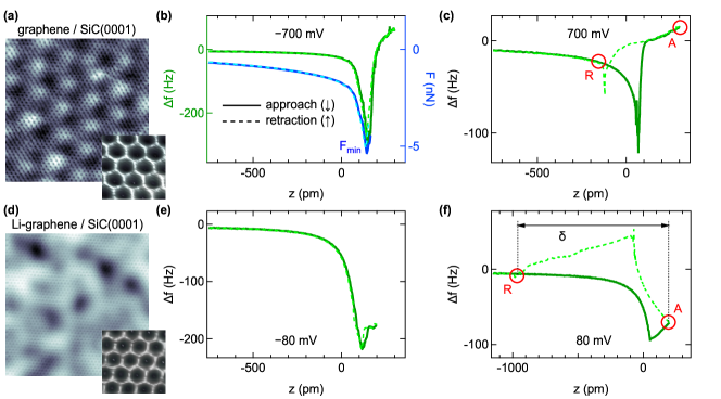
Figure 1 summarizes the first part of novel experimental results for clean [Fig. 1(a)–(c)] and Li-intercalated [Fig. 1(d)–(f)] graphene on SiC(0001) [11]. Clean graphene [Fig. 1(a)] yields STM images that are characterized by the previously reported superlattice with a spatial period of [12, 13] and the graphene lattice where the honeycomb cells are separated by , in agreement with expectations () [14]. For Li-intercalated graphene the superstructure is absent [Fig. 1(d)], signaling the efficient migration of Li through the Bernal-stacked graphene and C buffer layer on SiC(0001) [15, 16, 17].
Approaching the AFM tip towards the graphene lattice with and simultaneously recording the resonance frequency change, , of the oscillating tuning fork leads to the distance-dependent data set referred to as (: tip displacement) in the following and depicted as the upper solid line in Fig. 1(b). The associated vertical force [18, 19], , appears as the lower solid line. Care has been taken to show well-posed force data by appropriately adjusting the maximum probed distance range with respect to the position of inflection points in the extracted force [20]. The minimum signals the point of maximum attraction. Beyond contact the evolution of deviates from the expected Lennard-Jones behavior, which would exhibit a steep increase due to Pauli repulsion. Most likely, atomic relaxations of the junction geometry are the cause for the deviations. Retraction of the AFM tip gives rise to and data that are depicted as dashed lines in Fig. 1(b). Obviously, approach and retraction data virtually coincide, that is, and . Using the opposite polarity of [Fig. 1(c)] leads to a significantly different behavior of and . Rather than reaching a well defined minimum, abruptly changes its slope [21]. Commencing the tip retraction at point A, data do not reproduce in the contact region. The trace intersects at point R before coinciding with for further retraction giving rise to a loop.
A similar trend of and was observed for Li-intercalated graphene [Fig. 1(d)], i. e., and are essentially identical for [Fig. 1(e)] and strongly deviate from each other for [Fig. 1(f)]. The loop width spanned by the distance between A and R, , is, however, larger for Li-intercalated graphene than for its pristine counterpart.
The presented contact experiments are reproducible. Subsequent approach-retraction cycles using the same tip, and contact site yield virtually identical data and leave the structural integrity of tip and sample invariant [22]. Therefore, forming and breaking the covalent tip–graphene bond is reversible. Moreover, the current evolution across the junction exhibits a consistent loop behavior [21].
Before discussing the dependence of the loop, a tentative interpretation of the experimental observations shall be offered here and corroborated below by the simulations. It seems that the chemical bond formed upon tip approach at is strong enough to locally detach the graphene sheet upon tip retraction. Therefore, the data necessarily differ from for those distances where the graphene sheet is partially attached to the tip. The point where the loop closes [R in Fig. 1(c),(f)] would then correspond to the release of the lifted graphene. At , in contrast, and nearly coincide, i. e., the chemical bond formed between the tip and graphene is weak and easily broken by tip retraction – the graphene sheet remains on the surface and impedes the evolution of a loop.
To further characterize the behavior upon tip approach and retraction and its dependence on the polarity, several other aspects were explored and are presented as the second part of novel experimental results in Fig. 2. Figure 2(a),(b) compares for clean [Fig. 2(a)] and Li-intercalated [Fig. 2(b)] graphene for a variety of tips. The different tips are characterized by the magnitude of . Repeatedly performed field emission on and indentations into a Au substrate presumably cover the PtIr tip apex with Au and lead to different macroscopic tip shapes. Therefore, the long-range van der Waals interaction between tip and surface is altered, which is reflected by . Both samples exhibit an asymmetric evolution of with the sign of . Whilst vanishes for it starts to increase monotonically for . Moreover, stays comparably low for clean graphene. At , is still lower than [Fig. 2(a)]. For Li-intercalated graphene and a tip with similar force minimum as in the case of clean graphene, adopts nearly already at [Fig. 2(b)]. This effect is most likely caused by graphene being in its quasi-free state, which facilitates its detachment from the surface.
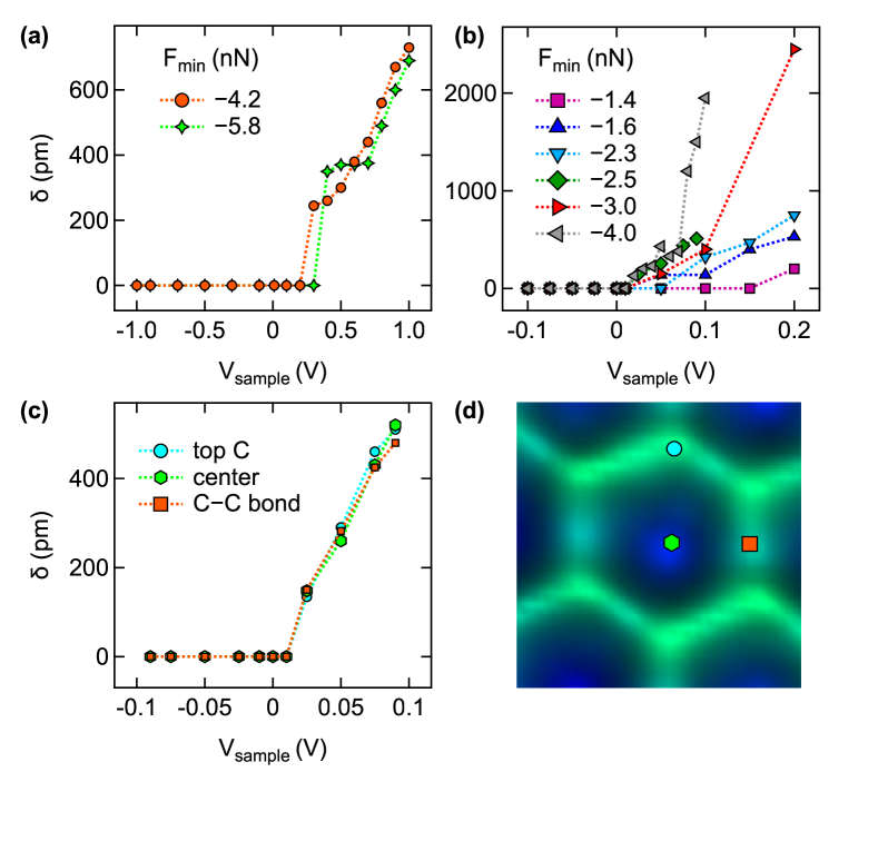
For the Li-intercalated sample, data obtained are collected in Fig. 2(b). A clear trend is visible. An increase of entails a larger slope of for , i. e., adopts large values already at low . This observation is plausible because the long-range van der Waals force acts as an additional background attraction and assists in lifting the graphene sheet [23, 24, 25]. The strength of the covalent tip–graphene bond, however, is determined by the short-range bond force, as clarified by the calculations below.
In a different set of experiments the graphene lattice site dependence of the characteristic behavior was explored. To this end, the high symmetry points of the honeycomb cell [a C atom, a C–C bond and a honeycomb center, Fig. 2(d)] were scrutinized. Despite the different lattice sites probed, is similar [Fig. 2(c)]. This observation indicates a preferred bond configuration that is achieved by relaxations of atom positions both at the tip apex and the graphene lattice and that is, therefore, a configuration adopted independent of the approach position. Selectively enhanced chemical reactivity of graphene C atoms on a metal surface were inferred previously from tunneling-to-contact transitions in STM junctions [26].
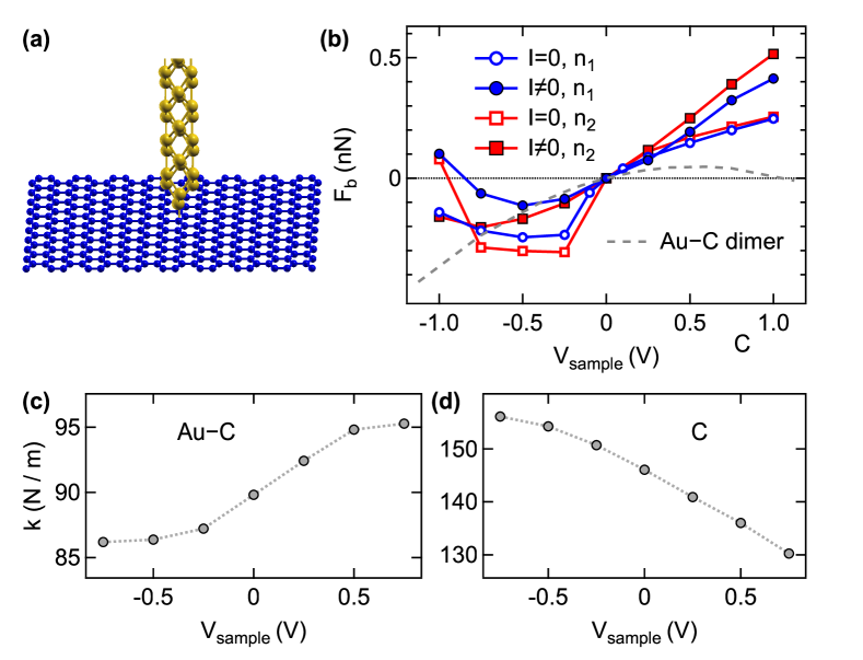
The density functional and transport calculations [27] were carried out for a simplified quasi-one-dimensional Au tip on top of a free finite graphene sheet [Fig. 3(a)] [28, 29]. They showed that the relaxation of the junction geometry prefers the top-C position to the hollow (by ) and bridge (by ) site of the graphene honeycomb cell. Consequently, independent of the tip position atop the graphene honeycomb cell a bond configuration in which the tip-terminating Au atom is positioned atop a C atom is preferred. This result is consistent with the experimental finding of a site-independent variation of with [Fig. 2(c)].
The atomic force induced by the applied field and the flowing current is calculated in the Born-Oppenheimer approximation and referred to as the bond force, , in the following. It is defined as the projection of onto , i. e., , with () the total force acting on the Au (C) atom and the vector from Au to C. The sign of is thus defined positive (negative) for attraction (repulsion).
In addition to the model setup [Fig. 3(a)] a Au–C dimer was considered in the calculations. Both configurations reveal an unambiguous asymmetry of with [Fig. 3(b)] – it is repulsive for and attractive for . This behavior applies to different electron doping levels as well as to the presence or absence of a current across the junction. In particular, all models reveal similar magnitudes and a bond strengthening for positive , while deviations arise mainly due to the different system sizes. For the calculated data reveal a slightly larger for than for . The higher -doping yields a stronger screening in graphene which tends to increase the voltage drop and local electric field at the Au–C contact. This calculated result is compatible with the experimental observation of a more pronounced loop for Li-intercalated graphene.
The sample voltage asymmetry of entails a corresponding asymmetry of the Au–C bond strength, which is plotted as the Au–C spring constant, , in Fig. 3(c). To obtain , the tip was displaced at constant and the change in evaluated. The increased at supports the idea of graphene detachment upon tip retraction. The detachment scenario is further corroborated by the evolution of the spring constant of a graphene C atom, , with [Fig. 3(d)], which was obtained by the finite displacement of the C atom along the surface normal. For increasing , becomes significantly smaller. Therefore, the C atom is more easily moved due to the attraction to the Au atom for than for .
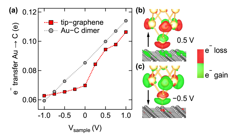
An important question to be answered concerns the origin of the asymmetry of . The charge transfer in the Au–C dimer [dots in Fig. 4(a)] as well as between the Au tip and graphene (squares) was calculated in a Hirshfeld charge analysis [30]. At , i. e., at zero electric field, electrons are transferred from (less electronegative) Au to (more electronegative) C of the dimer leading to an electric dipole [31]. For () electron transfer from Au to C is enhanced (reduced) compared to . For the tip–graphene model the electron transfer from the Au tip to graphene follows the same trend, with supporting the electron transfer from the Au tip to graphene, which accumulates positive charge at the tip apex and negative charge in the atomic environment of the contacted graphene C atom [Fig. 4(b)]. The zero-bias dipole is enhanced and the polar bond is strengthened for . For , in contrast, electron transfer from Au to C is hindered and accumulates the opposite charge at the atoms [Fig. 4(c)]. The polar bond is thus weakened. This field-driven – rather than current-induced – effect is consistent with the experimentally observed nearly point-symmetric current with respect to in a interval where the asymmetry of is already clearly visible [32]. Moreover, the calculated projected densities of states involving the relevant , , orbitals [33] clearly reveal the field-induced charge redistribution and show that positive (negative) tends to decrease (increase) the Au–C bond length [34]. This mechanism differs from the current-induced forces reported for homonuclear bonds [35, 36, 37, 38] where changes in bond strength were attributed to modifications in the overlap population caused by the nonequilibrium filling of scattering states, rather than to charge transfer and dipole field interaction between the components.
In conclusion, the combination of atomic force microscopy, density functional and nonequilibrium Green’s function calculations unveils that the archteypical polar bond between two atoms can individually be influenced by the magnitude and orientation of an external electric field. The control of a single polar chemical two-atom bond proceeds via the field-induced charge transfer between the atoms with different electronegativity. Tailoring chemical bond strengths at the single-atom level together with the possibility of applying and releasing mechanical load open the path to locally distort matter and explore its response. From a chemical point of view, reactivity and catalytic activity may be accessed at the atomic scale with the presented methods.
Acknowledgements.
Funding by the Deutsche Forschungsgemeinschaft (Grant No. KR 2912/10-3) and Villum Fonden (Grant No. 00013340) is acknowledged. The Center for Nanostructured Graphene (CNG) is sponsored by the Danish Research Foundation (Grant No. DNRF103).References
- Xin et al. [2019] N. Xin, J. Guan, C. Zhou, X. Chen, C. Gu, Y. Li, M. A. Ratner, A. Nitzan, J. F. Stoddart, and X. Guo, Nature Reviews Physics 1, 211 (2019).
- Wang et al. [2010] Y. F. Wang, J. Kröger, R. Berndt, H. Vázquez, M. Brandbyge, and M. Paulsson, Phys. Rev. Lett. 104, 176802 (2010).
- Schull et al. [2011] G. Schull, T. Frederiksen, A. Arnau, D. Sanchez-Portal, and R. Berndt, Nat. Nanotechnol. 6, 23 (2011).
- Gross et al. [2009] L. Gross, F. Mohn, N. Moll, P. Liljeroth, and G. Meyer, Science 325, 1110 (2009).
- de Oteyza et al. [2013] D. G. de Oteyza, P. Gorman, Y.-C. Chen, S. Wickenburg, A. Riss, D. J. Mowbray, G. Etkin, Z. Pedramrazi, H.-Z. Tsai, A. Rubio, M. F. Crommie, and F. R. Fischer, Science 340, 1434 (2013).
- Emmrich et al. [2015] M. Emmrich, F. Huber, F. Pielmeier, J. Welker, T. Hofmann, M. Schneiderbauer, D. Meuer, S. Polesya, S. Mankovsky, D. Ködderitzsch, H. Ebert, and F. J. Giessibl, Science 348, 308 (2015).
- Albrecht et al. [2015a] F. Albrecht, N. Pavliček, C. Herranz-Lancho, M. Ruben, and J. Repp, Journal of the American Chemical Society 137, 7424 (2015a).
- Hapala et al. [2014] P. Hapala, R. Temirov, F. S. Tautz, and P. Jelínek, Phys. Rev. Lett. 113, 226101 (2014).
- Albrecht et al. [2015b] F. Albrecht, J. Repp, M. Fleischmann, M. Scheer, M. Ondráček, and P. Jelínek, Phys. Rev. Lett. 115, 076101 (2015b).
- Ellner et al. [2016] M. Ellner, N. Pavliček, P. Pou, B. Schuler, N. Moll, G. Meyer, L. Gross, and R. Peréz, Nano Letters 16, 1974 (2016).
- pol [a] See Supplemental Material at [URL will be inserted by publisher], which includes Refs. [39, 40, 41, 42, 43], for experimental details on sample and tip preparation as well as data anlysis tools.
- Chang et al. [1991] C. Chang, I. Tsong, Y. Wang, and R. Davis, Surface Science 256, 354 (1991).
- Kim et al. [2008] S. Kim, J. Ihm, H. J. Choi, and Y.-W. Son, Phys. Rev. Lett. 100, 176802 (2008).
- N’Diaye et al. [2008] A. T. N’Diaye, J. Coraux, T. N. Plasa, C. Busse, and T. Michely, New J. Phys. 10, 043033 (2008).
- Virojanadara et al. [2010] C. Virojanadara, S. Watcharinyanon, A. A. Zakharov, and L. I. Johansson, Phys. Rev. B 82, 205402 (2010).
- Fiori et al. [2017] S. Fiori, Y. Murata, S. Veronesi, A. Rossi, C. Coletti, and S. Heun, Phys. Rev. B 96, 125429 (2017).
- Omidian et al. [2020] M. Omidian, N. Néel, E. Manske, J. Pezoldt, Y. Lei, and J. Kröger, Surface Science 699, 121638 (2020).
- Giessibl [2001] F. J. Giessibl, Appl. Phys. Lett. 78, 123 (2001).
- Sader and Jarvis [2004] J. E. Sader and S. P. Jarvis, Appl. Phys. Lett. 84, 1801 (2004).
- Sader et al. [2018] J. E. Sader, B. D. Hughes, F. Huber, and F. J. Giessibl, Nature Nanotechnology 13, 1088 (2018).
- pol [b] See Supplemental Material at [URL will be inserted by publisher], which includes Refs. [40, 41, 44, 42, 45], for the vertical-distance evolution of the current (Fig. S1, Fig. S2).
- pol [c] See Supplemental Material at [URL will be inserted by publisher] for the reversibility of chemical-bond formation (Fig. S3).
- Mashoff et al. [2010] T. Mashoff, M. Pratzer, V. Geringer, T. J. Echtermeyer, M. C. Lemme, M. Liebmann, and M. Morgenstern, Nano Letters 10, 461 (2010).
- Klimov et al. [2012] N. N. Klimov, S. Jung, S. Zhu, T. Li, C. A. Wright, S. D. Solares, D. B. Newell, N. B. Zhitenev, and J. A. Stroscio, Science 336, 1557 (2012).
- Wolloch et al. [2015] M. Wolloch, G. Feldbauer, P. Mohn, J. Redinger, and A. Vernes, Phys. Rev. B 91, 195436 (2015).
- Altenburg et al. [2010] S. J. Altenburg, J. Kröger, B. Wang, M.-L. Bocquet, N. Lorente, and R. Berndt, Phys. Rev. Lett. 105, 236101 (2010).
- pol [d] See Supplemental Material at [URL will be inserted by publisher], which includes Refs. [46, 47, 48, 49, 50, 51, 38, 28, 29, 52, 36, 17, 53], for theoretical details.
- Calogero et al. [2019] G. Calogero, N. Papior, M. Koleini, M. H. L. Larsen, and M. Brandbyge, Nanoscale 11, 6153 (2019).
- Papior et al. [2019] N. Papior, G. Calogero, S. Leitherer, and M. Brandbyge, Phys. Rev. B 100, 195417 (2019).
- Hirshfeld [1977] F. L. Hirshfeld, Theoretica chimica acta 44, 129 (1977).
- Rahm et al. [2019] M. Rahm, T. Zeng, and R. Hoffmann, Journal of the American Chemical Society 141, 342 (2019).
- pol [e] See Supplemental Material at [URL will be inserted by publisher] for current-voltage characteristics (Fig. S4).
- pol [f] See Supplemental Material at [URL will be inserted by publisher] for calculated projected densities of states (Fig. S5).
- pol [g] See Supplemental Material at [URL will be inserted by publisher] for calculated total energies (Fig. S6).
- Brandbyge et al. [2003] M. Brandbyge, K. Stokbro, J. Taylor, J.-L. Mozos, and P. Ordejón, Phys. Rev. B 67, 193104 (2003).
- Leitherer et al. [2019] S. Leitherer, N. Papior, and M. Brandbyge, Phys. Rev. B 100, 035415 (2019).
- Brand et al. [2019] J. Brand, S. Leitherer, N. R. Papior, N. Néel, Y. Lei, M. Brandbyge, and J. Kröger, Nano Letters 19, 7845 (2019).
- Kröger et al. [2020] J. Kröger, N. Néel, T. O. Wehling, and M. Brandbyge, Small Methods 4, 1900817 (2020).
- Giessibl [1998] F. J. Giessibl, Applied Physics Letters 73, 3956 (1998).
- Limot et al. [2005] L. Limot, J. Kröger, R. Berndt, A. Garcia-Lekue, and W. A. Hofer, Phys. Rev. Lett. 94, 126102 (2005).
- Kröger et al. [2008] J. Kröger, N. Néel, and L. Limot, J. Phys.: Condens. Matter 20, 223001 (2008).
- Berndt et al. [2010] R. Berndt, J. Kröger, N. Néel, and G. Schull, Phys. Chem. Chem. Phys. 12, 1022 (2010).
- Horcas et al. [2007] I. Horcas, R. Fernández, J. M. Gómez-Rodríguez, J. Colchero, J. Gómez-Herrero, and A. M. Baro, Rev. Sci. Instrum. 78, 013705 (2007).
- Néel et al. [2009] N. Néel, J. Kröger, and R. Berndt, Phys. Rev. Lett. 102, 086805 (2009).
- Néel et al. [2011] N. Néel, J. Kröger, and R. Berndt, Nano Letters 11, 3593 (2011).
- Soler et al. [2002] J. M. Soler, E. Artacho, J. D. Gale, A. García, J. Junquera, P. Ordejón, and D. Sánchez-Portal, J. Phys.: Condens. Matter 14, 2745 (2002).
- Brandbyge et al. [2002] M. Brandbyge, J.-L. Mozos, P. Ordejón, J. Taylor, and K. Stokbro, Phys. Rev. B 65, 165401 (2002).
- Papior et al. [2017] N. Papior, N. Lorente, T. Frederiksen, A. García, and M. Brandbyge, Comput. Phys. Commun. 212, 8 (2017).
- Papior [2018] N. Papior, sisl: v0.9.4 (2018).
- Perdew et al. [1996] J. P. Perdew, K. Burke, and M. Ernzerhof, Phys. Rev. Lett. 77, 3865 (1996).
- Halle et al. [2018] J. Halle, N. Néel, M. Fonin, M. Brandbyge, and J. Kröger, Nano Letters 18, 5697 (2018).
- Papior et al. [2016] N. Papior, T. Gunst, D. Stradi, and M. Brandbyge, Phys. Chem. Chem. Phys. 18, 1025 (2016).
- Caffrey et al. [2016] N. M. Caffrey, L. I. Johansson, C. Xia, R. Armiento, I. A. Abrikosov, and C. Jacobi, Phys. Rev. B 93, 195421 (2016).