Optical induced Spin Current in Monolayer NbSe2
Abstract
Monolayer NbSe2 is a metallic two-dimensional (2D) transition-metal dichalcogenide material. Owing to the lattice structure and the strong atomic spin-orbit coupling (SOC) field, monolayer NbSe2 possesses Ising-type SOC which acts as effective Zeeman field, leading to the unconventional topological spin properties. In this paper, we numerically calculate spin-dependent optical conductivity of monolayer NbSe2 using Kubo formula based on an effective tight-binding model which includes , and orbitals of Nb atom. Numerical calculation indicates that the up- and down-spin have opposite sign of Hall current, so the pure spin Hall current can be generated in monolayer NbSe2 under light irradiation, owing to the topological nature of monolayer NbSe2, i.e., finite spin Berry curvature. The spin Hall angle is also evaluated. The optical induced spin Hall current can be enhanced by the electron doping and persists even at room temperature. Our results will serve to design opt-spintronics devices such as spin current harvesting by light irradiation on the basis of 2D materials.
Transition-metal dichalcogenide (TMDC) is a new class of two-dimensional (2D) electronic systems and provides a platform to design new functional opt-electronic devices. Mak et al. (2010); Splendiani et al. (2010); Tongay et al. (2012); Gutiérrez et al. (2013); Zhao et al. (2013) In TMDC, electronic properties crucially depend on the combination of metal and chalcogen atoms. Wang et al. (2012); Chhowalla et al. (2013) Because of weak van der Waals forces between layers, monolayer of TMDC can be easily exfoliated and exhibit many fascinating properties such as valley-dependent optical selection rule Zeng et al. (2012); Mak et al. (2012); Cao et al. (2012); Yu et al. (2015) and spin Hall effect (SHE). Sinova et al. (2015); Hai (2020); Kato et al. (2004); Wunderlich et al. (2005) In particular, monolayer NbSe2 belongs to monolayer of group- TMDC MX2 (M=Nb, Ta; X=S, Se), and is known to show metallic behavior with superconducting phase transition at low temperature. Kim and Son (2017); He et al. (2018); Xi et al. (2016); Sohn et al. (2018) Monolayer NbSe2 has a hexagonal lattice structure but with no spatial inversion symmetry and possesses out-of-plane mirror symmetry. Owing to the lattice structure and strong atomic spin-orbit coupling (SOC) field, monolayer NbSe2 possesses Ising-type SOC, He et al. (2018); Xi et al. (2016); Sohn et al. (2018); Lu et al. (2015); Saito et al. (2016); Zhou et al. (2016); Bawden et al. (2016) i.e., effective Zeeman field that locks electron spin to out-of-plane directions by in-plane momentum and provides the unconventional topological spin properties.
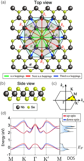
In this paper, we show that pure spin Hall current can be generated in monolayer NbSe2 by light irradiation, owing to the topological nature of monolayer NbSe2, i.e., finite spin Berry curvature. Figures 1 (a) and (b) show the top and side views of monolayer NbSe2, respectively, where a layer of Nb atoms is sandwiched by two layers of Se atoms. From top view, monolayer NbSe2 has a hexagonal lattice structure but with no spatial inversion symmetry. Also, from the side view, it respects out-of-plane mirror symmetry. Figure 1 (c) shows the corresponding first Brillouin Zone (BZ). We employ a multi-orbitals tight-binding model (TBM) which includes , and orbitals of Nb atom to describe the electronic states of NbSe2. He et al. (2018); Liu et al. (2013) The eigenvalue equation for TBM is where is the wavenumber vector, is the eigenvalue and is the band index. The eigenvector is defined as , where indicates the transpose of vector and means the amplitude at atomic orbital with spin for the th energy band at . The Hamiltonian with the SOC can be written as
| (1) |
with
| (2) |
and
| (3) |
Here, and are Pauli matrices, and is the Ising-type SOC parameter. In monolayer NbSe2, eV. includes the electron hoppings only among three -orbitals of Nb atoms, which are assumed up to third-nearest neighbor sites as shown in Fig. 1 (a). Here, green, red and blue arrows indicate hopping vectors pointing to nearest-neighbor (n.n) sites, the vectors pointing to next n.n sites and the vectors pointing to third n.n sites, respectively. The details of matrix elements , , , , and can be found in Supplementary material. sup Figure 1 (d) shows the energy band structure of monolayer NbSe2 along the line passing through the high-symmetric points of 1st BZ and the corresponding density of states (DOS). Here, red and blue lines indicate spin-up and spin-down states. Monolayer NbSe2 is metallic, but a large energy band gap between the partially filled valence bands and empty conduction bands. Also, the Ising-type SOC provides the opposite spin splitting at the valence band edges in K and K′ points, and time-reversal symmetry protection.
We numerically calculate spin-dependent optical conductivity of NbSe2 using Kubo formula Qiao et al. (2018); Guo et al. (2005); Sengupta et al. (2015); Vargiamidis et al. (2014); Tanaka et al. (2008); Ferreira et al. (2011); Morimoto et al. (2009); Yao et al. (2004); Li and Carbotte (2012); Akita et al. (2020) based on an effective TBM, and find the photo-induced generation of pure spin Hall current. Huang et al. (2020); Lin and Chien (2018); Shan et al. (2015) The spin-dependent optical Hall conductivity can be given as
| (4) |
where () indicates the band index including spin degree of freedom, is the eigen function with the eigen energy and is Fermi-Dirac distribution function. is infinitesimally small real number, and is the area of system. Also, is the spin current operator, and written as , where is the identity matrix and is the group velocity operator. We add the superscript for the spin-dependent optical Hall conductivity in order to distinguish its conductivity from ordinary optical Hall conductivity without SOC. When we consider for direct current (DC) limit (), zero-temperature ( K) and clean limit ( eV), Equation (14) becomes
| (5) |
with
| (6) |
Here, is spin Berry curvature of Bloch state, Qiao et al. (2018); Sławińska et al. (2019); Yao and Fang (2005); Da et al. (2020); Gradhand et al. (2012); Qu et al. (2019); Kim et al. (2019); Guo et al. (2008); Yao et al. (2004); Zhou et al. (2019) and drives an anomalous transverse velocity Feng et al. (2012); Xiao et al. (2010) written as
| (7) |
under the presence of an electric field .
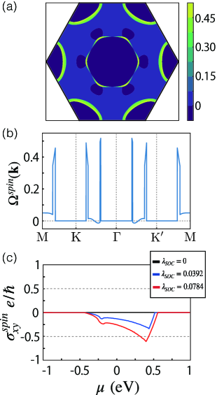
Figure 2 (a) shows the 2D contour plot of spin Berry curvature in 1st BZ. It clearly shows the six-fold symmetry. However, for each spin state, its symmetry around point reduces to three-fold symmetry because the energy band of monolayer NbSe2 has opposite spin splitting around K and K′ points [see Figs. S2 (a) and (b)]. sup In Fig. 2 (b), the spin Berry curvature is plotted along the path passing through high-symmetric points of 1st BZ. Owing to the Fermi-Dirac distribution function in Eq. (6), the spin Berry curvature is vanished at valleys. This is very contrast from semiconducting MX2 such as MoS2, where valley current is induced owing to the finite Berry curvature at the valleys. In monolayer NbSe2, valley current can be induced by the electron doping [see Figs. S4 (a) and (b)]. sup As can be seen in Fig. 2 (b), the spin Berry curvature has sharp peaks with the same sign, because the energy differences between up and down spin states become very small at the Fermi energy as can be confirmed in Fig. 1 (d). Figure 2 (c) shows Fermi energy dependence of spin-dependent Hall conductivity for several different SOC parameters. Since spin Hall conductivity is the summation of the spin Berry curvature over the momentum in DC limit, and can be calculated by using Eq. (5). It is noted that the spin Hall conductivity is enhanced by electron-doping. Thus, finite Berry curvature manifests the intrinsic SHE Zhou et al. (2019); Guo et al. (2008); Feng et al. (2012), i.e., the generation of transverse spin current by the application of electric field.
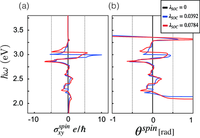
Figure 3 (a) shows the numerically calculated angular frequency dependence of spin-dependent optical Hall conductivity for several different SOC parameters. It is clearly seen that the large peak around eV, i.e., the generation of spin Hall current in NbSe2 ( eV) by light irradiation. The cases for and eV are also plotted for the comparison. It should be noted that the optical charge Hall conductivity is identically zero for arbitrary energy, because the charge Berry curvature has the anti-symmetric with the wave number, i.e., [see Figs. S2 (c) and (d)]. sup Thus, the pure spin current can be induced by light irradiation in monolayer NbSe2. Since the intensive peaks of appear in the range of eV, i.e., visible and ultraviolet range, monolayer NbSe2 can be used for the application of spin current harvesting by light irradiation. The effect of optical induced spin Hall current is also robust to temperature, and is expected to be observed even in room temperature [see Fig. S5 (a)]. sup
Figure 3 (b) shows the angular frequency dependence of spin Hall angle (SHA), Qiao et al. (2018); Zhou et al. (2019); Huang et al. (2020); Wang et al. (2014); Zhang et al. (2016) which measures conversion efficiency from charge current to spin current. SHA is given as
| (8) |
where is optical longitudinal conductivity Kubo (1957); Ferreira et al. (2011); Saberi-Pouya et al. (2017) which is found in Fig. S5 (b). sup SHA has divergence below about eV and above about eV, because becomes zero, where SHA becomes ill-defined. When the Hall conductivity has peak, the SHA also has larger value and then indicates that we can generate the pure spin current efficiently. Moreover, the observed optical induced pure Hall spin current is robust against the carrier doping. In particular, the pure spin current can be enhanced by electron-doping [see Fig. S6]. sup These results indicate that we can generate the spin Hall current efficiently by light irradiation using visible light of violet and enhance its magnitude by electron doping.
In conclusion, we have theoretically proposed that pure spin Hall current can be induced efficiently in monolayer NbSe2 by irradiating the visible light. The origin of spin Hall current can be attributed by the finite spin Berry curvature owing to the Ising-type SOC in monolayer NbSe2. It is also found that the optical induced spin Hall current can be enhanced by the electron doping and persists even in the room temperature[see Supplementary material]. sup Thus, monolayer NbSe2 can be used for the source of pure spin current by using light irradiation. Our results will serve to design opt-spintronics devices such as spin current harvesting by light irradiation on the basis of 2D materials.
This work was supported by JSPS KAKENHI (Nos. JP21H01019, JP18H01154) and JST CREST (No. JPMJCR19T1).
References
- Mak et al. (2010) K. F. Mak, C. Lee, J. Hone, J. Shan, and T. F. Heinz, Phys. Rev. Lett. 105, 136805 (2010).
- Splendiani et al. (2010) A. Splendiani, L. Sun, Y. Zhang, T. Li, J. Kim, C.-Y. Chim, G. Galli, and F. Wang, Nano Lett. 10, 1271 (2010).
- Tongay et al. (2012) S. Tongay, J. Zhou, C. Ataca, K. Lo, T. S. Matthews, J. Li, J. C. Grossman, and J. Wu, Nano Lett. 12, 5576 (2012).
- Gutiérrez et al. (2013) H. R. Gutiérrez, N. Perea-López, A. L. Elías, A. Berkdemir, B. Wang, R. Lv, F. López-Urías, V. H. Crespi, H. Terrones, and M. Terrones, Nano Lett. 13, 3447 (2013).
- Zhao et al. (2013) W. Zhao, Z. Ghorannevis, L. Chu, M. Toh, C. Kloc, P.-H. Tan, and G. Eda, ACS Nano 7, 791 (2013).
- Wang et al. (2012) Q. H. Wang, K. Kalantar-Zadeh, A. Kis, J. N. Coleman, and M. S. Strano, Nat. Nanotechnol. 7, 699 (2012).
- Chhowalla et al. (2013) M. Chhowalla, H. S. Shin, G. Eda, L.-J. Li, K. P. Loh, and H. Zhang, Nat. Chem. 5, 263 (2013).
- Zeng et al. (2012) H. Zeng, J. Dai, W. Yao, D. Xiao, and X. Cui, Nat. Nanotechnol. 7, 490 (2012).
- Mak et al. (2012) K. F. Mak, K. He, J. Shan, and T. F. Heinz, Nat. Nanotechnol. 7, 494 (2012).
- Cao et al. (2012) T. Cao, G. Wang, W. Han, H. Ye, C. Zhu, J. Shi, Q. Niu, P. Tan, E. Wang, B. Liu, and J. Feng, Nat. Commun. 3, 887 (2012).
- Yu et al. (2015) H. Yu, X. Cui, X. Xu, and W. Yao, Natl. Sci. Rev. 2, 57 (2015).
- Sinova et al. (2015) J. Sinova, S. O. Valenzuela, J. Wunderlich, C. H. Back, and T. Jungwirth, Rev. Mod. Phys. 87, 1213 (2015).
- Hai (2020) P. N. Hai, J. Magn. Soc. Jpn. 44, 137 (2020).
- Kato et al. (2004) Y. K. Kato, R. C. Myers, A. C. Gossard, and D. D. Awschalom, Science 306, 1910 (2004).
- Wunderlich et al. (2005) J. Wunderlich, B. Kaestner, J. Sinova, and T. Jungwirth, Phys. Rev. Lett. 94, 047204 (2005).
- Kim and Son (2017) S. Kim and Y.-W. Son, Phys. Rev. B 96, 155439 (2017).
- He et al. (2018) W.-Y. He, B. T. Zhou, J. J. He, N. F. Q. Yuan, T. Zhang, and K. T. Law, Commun. Phys. 1, 40 (2018).
- Xi et al. (2016) X. Xi, Z. Wang, W. Zhao, J.-H. Park, K. T. Law, H. Berger, L. Forró, J. Shan, and K. F. Mak, Nat. Phys. 12, 139 (2016).
- Sohn et al. (2018) E. Sohn, X. Xi, W.-Y. He, S. Jiang, Z. Wang, K. Kang, J.-H. Park, H. Berger, L. Forró, K. T. Law, J. Shan, and K. F. Mak, Nat. Mater. 17, 504 (2018).
- Lu et al. (2015) J. M. Lu, O. Zheliuk, I. Leermakers, N. F. Q. Yuan, U. Zeitler, K. T. Law, and J. T. Ye, Science 350, 1353 (2015).
- Saito et al. (2016) Y. Saito, Y. Nakamura, M. S. Bahramy, Y. Kohama, J. Ye, Y. Kasahara, Y. Nakagawa, M. Onga, M. Tokunaga, T. Nojima, Y. Yanase, and Y. Iwasa, Nat. Phys. 12, 144 (2016).
- Zhou et al. (2016) B. T. Zhou, N. F. Q. Yuan, H.-L. Jiang, and K. T. Law, Phys. Rev. B 93, 180501(R) (2016).
- Bawden et al. (2016) L. Bawden, S. P. Cooil, F. Mazzola, J. M. Riley, L. J. Collins-McIntyre, V. Sunko, K. W. B. Hunvik, M. Leandersson, C. M. Polley, T. Balasubramanian, T. K. Kim, M. Hoesch, J. W. Wells, G. Balakrishnan, M. S. Bahramy, and P. D. C. King, Nat. Commun. 7, 11711 (2016).
- Liu et al. (2013) G.-B. Liu, W.-Y. Shan, Y. Yao, W. Yao, and D. Xiao, Phys. Rev. B 88, 085433 (2013).
- (25) See Supplemetary Material at [URL will be inserted by publisher] for details of matrix elements in an effective Hamiltonian. It is also presented the doping and temperature effects on optical spin Hall conductivity.
- Qiao et al. (2018) J. Qiao, J. Zhou, Z. Yuan, and W. Zhao, Phys. Rev. B 98, 214402 (2018).
- Guo et al. (2005) G. Y. Guo, Y. Yao, and Q. Niu, Phys. Rev. Lett. 94, 226601 (2005).
- Sengupta et al. (2015) P. Sengupta, S. Rakheja, and E. Bellotti, arXiv:1512.06734 (2015).
- Vargiamidis et al. (2014) V. Vargiamidis, P. Vasilopoulos, and G.-Q. Hai, J. Phys. Condens. Matter 26, 345303 (2014).
- Tanaka et al. (2008) T. Tanaka, H. Kontani, M. Naito, T. Naito, D. S. Hirashima, K. Yamada, and J. Inoue, Phys. Rev. B 77, 165117 (2008).
- Ferreira et al. (2011) A. Ferreira, J. Viana-Gomes, Y. V. Bludov, V. Pereira, N. M. R. Peres, and A. H. Castro Neto, Phys. Rev. B 84, 235410 (2011).
- Morimoto et al. (2009) T. Morimoto, Y. Hatsugai, and H. Aoki, Phys. Rev. Lett. 103, 116803 (2009).
- Yao et al. (2004) Y. Yao, L. Kleinman, A. H. MacDonald, J. Sinova, T. Jungwirth, D.-s. Wang, E. Wang, and Q. Niu, Phys. Rev. Lett. 92, 037204 (2004).
- Li and Carbotte (2012) Z. Li and J. P. Carbotte, Phys. Rev. B 86, 205425 (2012).
- Akita et al. (2020) M. Akita, Y. Fujii, M. Maruyama, S. Okada, and K. Wakabayashi, Phys. Rev. B 101, 085418 (2020).
- Huang et al. (2020) S. Y. Huang, D. Qu, T. C. Chuang, C. C. Chiang, W. Lin, and C. L. Chien, Appl. Phys. Lett. 117, 190501 (2020).
- Lin and Chien (2018) W. Lin and C. L. Chien, arXiv:1804.01392 (2018).
- Shan et al. (2015) W.-Y. Shan, J. Zhou, and D. Xiao, Phys. Rev. B 91, 035402 (2015).
- Sławińska et al. (2019) J. Sławińska, F. T. Cerasoli, H. Wang, S. Postorino, A. Supka, S. Curtarolo, M. Fornari, and M. B. Nardelli, 2D Mater. 6, 025012 (2019).
- Yao and Fang (2005) Y. Yao and Z. Fang, Phys. Rev. Lett. 95, 156601 (2005).
- Da et al. (2020) H. Da, Q. Song, P. Dong, H. Ye, and X. Yan, J. Appl. Phys. 127, 023903 (2020).
- Gradhand et al. (2012) M. Gradhand, D. V. Fedorov, F. Pientka, P. Zahn, I. Mertig, and B. L. Györffy, J. Phys. Condens. Matter 24, 213202 (2012).
- Qu et al. (2019) G. Qu, K. Nakamura, and M. Hayashi, arXiv:1901.05651 (2019).
- Kim et al. (2019) J. Kim, K.-W. Kim, D. Shin, S.-H. Lee, J. Sinova, N. Park, and H. Jin, Nat. Commun. 10, 3965 (2019).
- Guo et al. (2008) G. Y. Guo, S. Murakami, T.-W. Chen, and N. Nagaosa, Phys. Rev. Lett. 100, 096401 (2008).
- Zhou et al. (2019) J. Zhou, J. Qiao, A. Bournel, and W. Zhao, Phys. Rev. B 99, 060408(R) (2019).
- Feng et al. (2012) W. Feng, Y. Yao, W. Zhu, J. Zhou, W. Yao, and D. Xiao, Phys. Rev. B 86, 165108 (2012).
- Xiao et al. (2010) D. Xiao, M.-C. Chang, and Q. Niu, Rev. Mod. Phys. 82, 1959 (2010).
- Wang et al. (2014) Y. Wang, P. Deorani, X. Qiu, J. H. Kwon, and H. Yang, Appl. Phys. Lett. 105, 152412 (2014).
- Zhang et al. (2016) W. Zhang, W. Han, S.-H. Yang, Y. Sun, Y. Zhang, B. Yan, and S. S. P. Parkin, Sci. Adv. 2, e1600759 (2016).
- Kubo (1957) R. Kubo, J. Phys. Soc. Japan 12, 570 (1957).
- Saberi-Pouya et al. (2017) S. Saberi-Pouya, T. Vazifehshenas, T. Salavati-fard, M. Farmanbar, and F. M. Peeters, Phys. Rev. B 96, 075411 (2017).