Local and non-local quantum transport due to Andreev bound states
in finite Rashba nanowires with superconducting and normal sections
Abstract
We analyze Andreev bound states (ABSs) that form in normal sections of a Rashba nanowire that is only partially covered by a superconducting layer. These ABSs are localized close to the ends of the superconducting section and can be pinned to zero energy over a wide range of magnetic field strengths even if the nanowire is in the non-topological regime. For finite-size nanowires (typically m in current experiments), the ABS localization length is comparable to the length of the nanowire. The probability density of an ABS is therefore non-zero throughout the nanowire and differential-conductance calculations reveal a correlated zero-bias peak (ZBP) at both ends of the nanowire. When a second normal section hosts an additional ABS at the opposite end of the superconducting section, the combination of the two ABSs can mimic the closing and reopening of the bulk gap in local and non-local conductances accompanied by the appearance of the ZBP. These signatures are reminiscent of those expected for Majorana bound states (MBSs) but occur here in the non-topological regime. Our results demonstrate that conductance measurements of correlated ZBPs at the ends of a typical superconducting nanowire or an apparent closing and reopening of the bulk gap in the local and non-local conductance are not conclusive indicators for the presence of MBSs.
I Introduction
Majorana bound states (MBSs) have been of significant interest in condensed matter physics for over two decades, largely due to their potential application as topological qubits [1, 2, 3, 4, 5, 6, 7]. The prospective utilization of MBSs in quantum computation stems from their non-Abelian braiding statistics [8, 9, 10, 11, 12, 13, 14, 15]. Despite this intense interest there has been no conclusive experimental observation of these exotic properties to date.
The most mature experimental platform expected to host MBSs are Rashba nanowires (see Fig. 1), where the key differential-conductance signature associated with MBSs is a zero-bias peak (ZBP) that is stable for a wide range of magnetic field strengths. A ZBP is, however, by itself not a unique fingerprint of MBSs. Previously it was suggested that additional local conductance features can clarify the origin of such a ZBP, namely the quantization of the peak height at [16, 17, 18, 19, 20] and oscillations around zero energy that originate from the overlap of the two MBS wavefunctions at either end of the nanowire [21, 22, 23, 24, 25]. The ZBPs and their oscillations have been observed in past experiments [26, 27, 28, 29, 30, 31, 32], while quantization of the ZBP has not been observed. Recently it has been suggested [33, 34] that the next generation of Rashba nanowire systems, three-terminal devices, could elucidate whether a given ZBP stems from the presence of MBSs by observing additional auxiliary features in the local and non-local differential conductances. For example, such devices could observe correlations between ZBPs at both ends of the nanowire and the closing and reopening of the bulk-gap that should accompany the transition to topological superconductivity.
l-0.03int-0.in(a)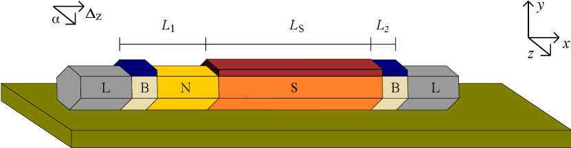
l-0.03int0.in(b)
Additional signatures of MBSs beyond a simple ZBP are necessary because topologically trivial states such as Andreev bound states (ABSs) [35, 36, 37, 38, 39, 40, 41, 42] can generate conductance features similar to those expected from MBSs and therefore strongly challenge the interpretation of experimental observations [43, 44, 45, 46, 47, 48, 49, 50, 51, 52, 53, 54, 55, 42, 56, 57]. For instance, it has been shown that the energy of an ABS in a non-topological system can be pinned close to zero over a wide range of magnetic field strengths when a resonance condition for the strength of the spin-orbit interaction (SOI) is fulfilled [48]. In transport experiments, this resonance is broadened by finite temperature and the coupling to external leads. Such ABSs can therefore produce ZBP features in the conductance even in systems that are topologically trivial at all magnetic field strengths. The pinning of trivial ABSs close to zero energy can also originate from smooth parameter profiles of the chemical potential and the superconducting gap [50, 49, 51], such that a short section of the nanowire is nominally in the topological regime. Such zero-energy states, observed in the trivial phase of the bulk of the nanowire, are known as quasi-Majorana bound states (quasi-MBSs) and their zero-bias pinning is in fact also stable against changes of SOI strength or tunnel barrier gate voltage.
Previous devices focussed on local measurements on a single end of a nanowire. Such measurements can already provide additional indicators that could clarify the origin of a ZBP. One example is the oscillations around zero energy expected due to the hybridization of MBSs at either end of a finite nanowire [21, 22, 23, 24]. Such oscillations should have an increasing amplitude when magnetic field strength is increased or nanowire length decreased. In contrast to this expectation, several experiments observed oscillations with an amplitude which decays as the magnetic field is increased [31, 58, 59]. Although there are proposed explanations for this behaviour such as orbital effects [24] or a step-like profile of the Rashba SOI strength [60], even in such scenarios the parameter window for a decay in the amplitude of oscillations is rather small and therefore the experimentally observed behaviour is likely the result of trivial states. In addition, recent theoretical works have shown that even the quantization of a ZBP at one end of the nanowire is not an exclusive property of MBSs [51, 61]. As such, while conductance oscillations and even quantization can provide limited additional evidence for the potential presence of MBSs, they are not sufficient for an unambiguous identification of topologically protected states.
Given the ambiguous origins of previous experimental observations from the single end of a nanowire, in the absence of braiding experiments, further signatures in conductance are necessary to improve the classification of ZBPs in the next generation of Rashba nanowire systems. For instance, this can be achieved by considering non-local correlation properties of MBSs in three-terminal devices [62, 63, 64, 33, 65, 66, 67, 68, 34]. MBSs should be localized at the opposite ends of a superconducting Rashba nanowire and therefore conductance measurements on both ends should reveal ZBPs. Furthermore, three-terminal experiments enable the measurement of non-local conductances which can indicate the bulk-gap closing and reopening and therefore go beyond local properties. Recently, it was highlighted in Ref. [33] that the exponential decay of sub-gap states into the bulk of the nanowire makes the non-local conductance an ideal tool for distinguishing between trivial and topological phases in nanowires which are much longer than the localization length of such sub-gap states. Recent experiments have been performed on three-terminal devices [69, 70, 71] but so far did not find clear signatures of MBSs.
In this paper we focus mainly on non-topological three-terminal junctions consisting of a partially proximitized Rashba nanowire where the normal sections can host an ABS. We consider normal-superconducting (NS) and normal-superconducting-normal (NSN) junction setups. In contrast to previous works, we examine the case where the ratio between the length of the superconducting section and the localization length of ABSs is small. This regime is of present experimental relevance and the nanowire lengths as well as the superconducting gaps we consider will be comparable to current setups where typical lengths are between m [71] and m [70]. The nanowire length is limited by the requirement of working in the ballistic regime to avoid disorder effects, which were shown to be harmful for the observation of topological phases. In the short-nanowire regime the wavefunction of a trivial ABS leaks from one end of the nanowire to the opposite end. When the parameters of the ABS are close to the resonance condition from Ref. [48], the energy of the ABS is pinned close to zero over a wide range of magnetic field strengths. Our calculation of the differential conductance confirms that in such a scenario correlated ZBPs of a trivial origin appear at both ends of the nanowire. We find that the same effect can occur for quasi-MBSs in topological nanowires.
We also examine the consequences of the presence of a second normal section hosting an additional ABS on the other side of the superconducting section. Such NSN junctions with two normal sections are expected to naturally occur in three-terminal devices available experimentally. We find that the appearance of the second ABS can further complicate the interpretation of experimental signatures. Not only is the second ABS also visible in the non-local conductance but the combination of the two ABSs at either end of the nanowire can generate a conductance feature that is reminiscent of the bulk-gap edge undergoing a closing and reopening process that should accompany a topological phase transition.
Our findings show that, while three-terminal devices can potentially provide additional insights into the origins of ZBPs, correlated zero-bias peaks at both ends of superconducting sections of Rashba nanowires and the apparent observation of the closing and reopening of the bulk band gap with increasing magnetic field strength do not suffice as unambiguous additional indicators for the presence of MBSs in nanowires of the lengths used in current experimental devices.
The paper is organized as follows. In Sec. II we define the model to describe a non-topological and a topological nanowire containing trivial zero-energy ABSs or quasi-MBSs, respectively. In Sec. III, we discuss features in the differential conductance arising due to the presence of a single ABS hosted in the, say, left normal section of a non-topological nanowire. Here we show that as the ratio between the length of the superconducting section and the localization length of the ABS is decreased, the probability density of the ABS on the right side of the nanowire increases and, as a result, the ABS also becomes visible in the local conductance measured at the right end of the nanowire. Moreover, we examine the case of an NSN junction with two normal sections, one at each end of the non-topological proximitized nanowire, and show that this setup can mimic the signatures of a topological phase transition in transport measurements, despite the trivial nature of the ABSs. Section IV focuses on the topological nanowire and addresses features arising due to the presence of quasi-MBSs in the left and right local conductance. It is shown again that if the ratio between the superconducting section and the localization length of the quasi-MBS is small, then correlated zero-bias peaks appear at both ends. Furthermore, we examine the non-local differential conductance via the bulk states undergoing the bulk-gap closing and reopening process when two normal sections at each end of the topological nanowire both host quasi-MBSs. Finally, we discuss the impact of our results on the interpretation of present-day three-terminal experiments in Sec. V. In App. A we describe numerical approaches used to model transport experiments. We compare the conductance pattern of the non-topological nanowire with the conductance pattern of a uniform topological nanowire in App. B. The effect of strong broadening of finite-energy peaks is discussed in App. C. In App. D we study the bulk wavefunctions of a topological nanowire with quasi-MBSs on both ends. Finally, App. E deals with the conductance pattern of a nanowire hosting quasi-MBSs on the left end and an ABS on the right end.
II Model of the nanowire
We consider a one-dimensional (1D) semiconducting nanowire aligned along the -direction. The system is subjected to a magnetic field, which is applied parallel to the nanowire axis. This magnetic field results in a Zeeman energy of strength . The nanowire is partially covered by an -wave superconductor, resulting in a proximity-induced superconducting gap in a section of length . This grounded superconducting section is centered between a left and a right normal section of length and , respectively. The Rashba SOI of strength is position-dependent and the corresponding SOI vector points in -direction. The effective 1D lattice Hamiltonian is given by
| (1) |
where and creates and annihilates an electron of spin at the lattice site , respectively. The total number of sites is given by , where , , and , where is an effective lattice constant. In addition, and denote the nearest neighbor tunneling matrix element and the chemical potential, respectively. Furthermore, denotes the Kronecker delta. Normal leads are attached on the left and right ends of the nanowire. The leads are modeled by the same Hamiltonian as the normal sections. The chemical potentials and of the left and right normal lead are adjusted to account for a possible difference between lead and nanowire. Additionally, we introduce tunnel barriers between the leads and the nanowire, these barriers of length and are constituent parts of the normal sections of length and , see Fig. 1b. The height of the tunnel barrier at site is used to control the coupling between the system and the leads, it therefore controls the conductance value. We will focus on two setups, which we refer to as the ‘non-topological’ and ‘topological’ nanowire. Both of these systems can host ABSs that are pinned to zero energy, however, the mechanism fixing the ABS energy to zero is different for the two nanowire types. These specific parameter configurations for the non-topological and topological cases are described in the following subsections II.1 and II.2.
l-0.03int-0.03in(a)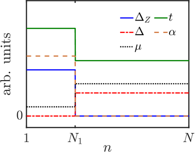
l-0.03int-0.03in(b)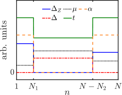
l-0.03int-0.03in(c)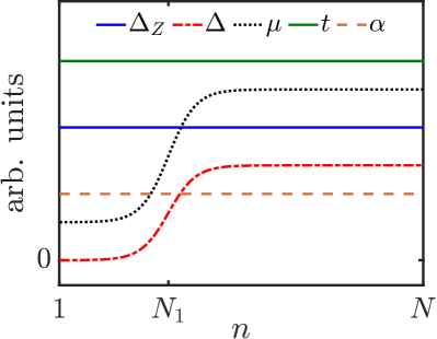
l-0.03int-0.03in(d)
II.1 Non-topological nanowire
In this section we specify the profiles of the parameters that enter the Hamiltonian, , given in Eq. (1) for the non-topological nanowire. We define the boundary between the left normal section () and the superconducting section (S) as and similarly the boundary between S and the right normal section () as . The non-uniform system parameters entering the Hamiltonian have the following structures: The tunneling matrix element is defined as
| (2) |
and is constructed out of the tunneling matrix elements in and and the tunneling matrix element in S. We define the Heaviside function with throughout. The difference between the tunneling matrix elements of the superconducting and the normal sections arises due to the mass renormalization inside the superconducting section caused by metallization effects induced by the thin superconducting shell [72, 73, 74, 75, 76, 77]. The chemical potential has a similar structure
| (3) |
where and denote the chemical potential in the normal sections and the chemical potential in the superconducting section. Since the magnetic field suppresses the bulk-gap of the parent superconductor, the superconducting gap decreases with increasing Zeeman energy and vanishes at the critical field strength :
| (4) |
where the maximal value is given by . Therefore, the superconducting gap has the following profile
| (5) |
The superconducting gap is zero in and . In contrast, the Zeeman energy and Rashba SOI are non-zero only in the normal sections and are defined as
| (6) | |||
| (7) |
Here, the SOI strengths and could be different [78]. The SOI energy is given by . In Fig. 2 we show examples of the profiles of the superconducting gap, the Zeeman energy, the chemical potential, the tunneling matrix element, and the Rashba SOI strength for an NS and an NSN junction. Tunnel barriers are described by
| (8) |
where and denote the height of the left and right tunnel barriers and and are the positions at which the left tunnel barrier ends and the right tunnel barrier starts, respectively. Here we defined via . We note that the topological phase cannot be achieved in this setup because the Zeeman energy and the Rashba SOI vanish in the superconducting section. We therefore refer to this system as non-topological nanowire.
II.2 Topological nanowire
The second system under consideration is a nanowire in which the chemical potential and the superconducting gap change smoothly. These smooth parameter variations can generate an ABS which, as in the non-topological nanowire, sticks to zero energy over a wide range of Zeeman energies in the trivial regime inside the superconducting section [43, 50, 49, 51]. In this case, nominally, the system enters the topological phase locally at the short segment between the normal and superconducting sections. However, the length of this segment is much shorter than the localization length of potential MBSs, such that only quasi-MBSs can appear in the spectrum if certain conditions are satisfied. The spatial dependence of parameters is modelled by the function
| (9) |
where parametrizes the smoothness (see Fig. 2c-d). The exact form of the function is not relevant for the appearance of quasi-MBSs rather it is the smoothness itself that determines the presence of quasi-MBSs. The superconducting gap (chemical potential) profile is characterized by the parameter (), which can take different values on the left and the right side of the nanowire:
| (10) | |||
| (11) |
In contrast to the previous section, here, we use a superconducting gap that is independent of the Zeeman energy. For the case of a single normal section on the left and a tunnel barrier only on the right, we choose the profiles:
| (12) | |||
| (13) |
The tunnel barriers are modeled in the same manner as in the non-topological system, see Eq. (8). The remaining parameters are chosen to be uniform:
| (14) |
In Figs. 2c and 2d, we show examples of profiles for the superconducting gap, the Zeeman energy, the chemical potential, the tunneling matrix element, and the Rashba SOI strength in an NS and an NSN junction. This system can enter a topological phase hosting MBSs, however, we will mainly focus on the trivial regime which can host only quasi-MBSs.
III ABS in Non-topological nanowires
III.1 ABS in the left normal section
In this section we study ABSs in non-topological nanowires as defined in Sec. II.1. We start our investigation with the setup shown in Fig. 1a but without tunnel barriers or leads. The left (right) normal section can host ABSs localized close to (). The ratio determines the ABS level spacing and therefore the number of ABSs in the left () and right () normal sections. If this ratio is large in comparison to as is in our case, then the system hosts only a few or a single ABS. The energy of the ABS is pinned to zero if the parameters approximately fulfill the resonance condition
| (15) |
where denotes the SOI momentum and denotes the effective electron mass inside the normal section [48]. The resonance condition is derived for a chemical potential equal to zero in the normal section, where it is calculated from the SOI energy. The ABS energy, however, can also be pinned to zero in the case of a non-zero chemical potential inside the normal section as we will demonstrate below numerically. In particular, we discuss both the energy spectrum as well as wavefunctions of the ABS. The wavefunction contains information about the spatial distribution of the ABS, which is important for understanding the local and non-local differential conductance of ABSs in three-terminal devices. The parameter profiles for the NS junction are shown in Fig. 2a. We examine the case of small ratios between the length of the superconducting section and the localization length of the ABSs,
| (16) |
Here, the renormalized Fermi velocity is defined as with being the effective mass in the superconducting section and the dependence of on is defined in Eq. (4). The value of is small for a short superconducting section or for a small superconducting gap . The latter is associated with a large localization length since is inverse proportional to .
l-0.02int0.0in(a)\stackinsetl1.7int0.0in(b)\stackinsetl-0.02int1.35in(c)\stackinsetl1.7int1.35in(d)
l0.0int0.02in(a)\stackinsetl1.8int0.02in(b)\stackinsetl-0.00int1.17in(c)\stackinsetl1.8int1.17in(d)\stackinsetl0int2.34in(e)\stackinsetl1.8int2.34in(f)\stackinsetl0int3.51in(g)\stackinsetl1.8int3.51in(h)
In Figs. 3a and 3b we plot the energy of the lowest ABS as a function of the SOI momentum and of the chemical potential with the Zeeman energy being fixed close to . For the ABS energy exhibits an oscillatory behavior that approximately matches the resonance condition from Eq. (15). The oscillatory behavior is preserved for and there are still recurring points at which the energy is close to zero (blue). Tuning the system to one of these resonance points also for finite values of the chemical potential (e.g. the orange or red square), we find a zero-energy pinning (see Figs. 3c and 4a). If the resonance points do not coincide for the different Zeeman energies (see the black square), then the energy is not strictly pinned to zero, see Fig. 3d. In a transport experiment, however, such small deviations from zero energy could be masked by, for example, finite temperature, resulting in a broadened ZBP (see App. C).
When the ratio between the length of the superconducting section and the localization length is large (), the exponential decay of the ABS wavefunction in the superconducting section means that the ABS is essentially entirely localized on the left side of the nanowire, see Fig. 4b. We extract the localization length of the ABS from the numerically calculated probability density, see Fig. 4b, and find that the numerical value of agrees well with the prediction of the analytic expression from Eq. (16). A smaller can be achieved by choosing a smaller superconducting gap (see Figs. 4c and 4d) or decreasing the length of the superconducting section (see Figs. 4e and 4f). TAs the parameter approaches one, the exponential suppression becomes less pronounced. his results in a small but finite probability density on the right end of the nanowire. We note that the probability density of the ABS on the right side is always non-zero for large values of the Zeeman energy when the superconducting gap is suppressed, see Fig. 4h. This behavior is explained by the dependence of the localization length on the Zeeman energy. The localization length increases for large Zeeman energies and therefore the parameter approaches the value . In addition, we note that the extended wavefunction of the ABS in nanowires with small values of can be expected to generate a signature in the local conductance measurements on both ends of the nanowire. These local signals on the left and right end would be correlated since they correspond to the same ABS. Experiments may therefore not be able to distinguish between this correlated ABS signatures and MBS signatures, when the parameter is small.
l-0.02int0.02in(a)\stackinsetl1.75int0.02in(b)\stackinsetl-0.02int1.07in(c)\stackinsetl1.75int1.07in(d)\stackinsetl-0.02int2.1in(e)\stackinsetl1.75int2.1in(f)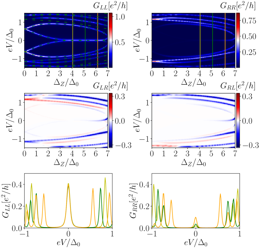
Next, we calculate numerically the differential-conductance matrix elements , which are the derivative of the current α in lead into the nanowire with respect to the voltage bias at lead (we follow the notation of Ref. [66], see App. A). To account for tunnel barriers and leads at both ends, see Fig. 1a, we choose a slightly longer normal section than before. The local conductance on the left end exhibits very similar features as the energy spectrum, which we plot for comparison as dark green dashed lines, see Fig. 5a. The ABS is visible for all Zeeman energies and is pinned close to zero for a wide range of but the conductance is not quantized to at zero bias and depends on the tunnel barrier properties such as its strength and length, which would be also a case for MBSs. Current experiments do not observe the quantized value, , of the ZBP expected for an MBS, thus, experiments cannot easily distinguish between this trivial feature and an MBS signature. A weaker ZBP also appears in for and stays stable until the superconducting gap is suppressed at , see also the line-cuts in Fig. 5f. This ZBP only appears for large Zeeman energies when the wavefunction starts to leak through the superconducting section. An equivalent signature could also be expected for the MBS case, for instance, when the two tunnel barriers are of different strength.
The non-local conductances and are similar to each other and exhibit the bulk-gap closing at as well as the ZBP, see Fig. 5. This ZBP in the non-local conductance is not present in long nanowires but it is visible in short wires due to the extension of the ABS over the entire superconducting section. We note that non-zero non-local conductances indicate that the local conductances and are not symmetric with respect to the bias, since electrons might tunnel directly between the normal leads, see Refs. [66, 67]. The sum of all differential-conductance matrix elements, however, is symmetric with respect to the bias. The antisymmetric part of the local conductance () corresponds to the negative value of the antisymmetric part of the non-local conductance (), see Ref. [66].
The ZBP in our setup is robust against changes of the Zeeman energy but not against fluctuations of the tunnel barrier strength . Indeed, tuning to slightly different values removes the perfect zero-energy pinning. Parenthetically we note that in short topological nanowires, the MBS wavefunctions overlap, and so, similar to the behavior of our ABSs, it is anyway expected that MBSs are not fixed to zero energy in short wires. Furthermore, broadening effects, for example due to temperature, affect the differential conductance. If the energy is not perfectly pinned to zero and the broadening is large enough then a conductance measurement can not resolve a small finite energy splitting and will reveal only a single peak, which actually consists of two single merged peaks around zero bias, see App. C. Although our system is not designed to explain the data from any specific experiment, we note that our results are similar to the experimental data from Ref. [71]. In particular, a ZBP appears in the left conductance for a specific value of the tunnel barrier gate voltage whereas a ZBP appears in the right conductance at larger Zeeman energies.
We conclude that such an ABS mimics certain key properties of an MBS, which, in turn, presents a challenge for an unambiguous interpretation of experimental observations. If the ratio between the length of the superconducting section and the localization length is small, then the ABS-ZBPs can even be correlated at the left and right ends of the nanowire. The ABS requires some tuning and is not universally stable against fluctuations in the SOI strength or the tunnel barrier strength. We again note that, by construction, the system considered in this section cannot enter the topological phase and so all features we have found here are due to trivial ABSs.
III.2 ABS in the left and right normal sections
In this section, we examine the non-topological nanowire with two normal sections hosting two ABSs: one on the left and another one on the right side of the nanowire, see Fig. 1b. As before we begin without tunnel barriers and without the leads. If the resonance condition is fulfilled simultaneously in the left and the right normal sections of the long nanowire, then the two ABSs become degenerate. The probability density shows peaks at both ends of the nanowire, see Fig. 6b. For long wires there is no correlation between the ABS on the left end and the ABS on the right end: both are independent of each other and the overlap of their wavefunctions is approximately zero. As can be expected from the previous section, this is not the case for shorter wires and correlations can occur when the ratio is small.
l0.0int0.02in(a)\stackinsetl1.7int0.02in(b)\stackinsetl-0.00int1.17in(c)\stackinsetl1.7int1.17in(d)\stackinsetl0int2.34in(e)\stackinsetl1.7int2.34in(f)\stackinsetl0int3.51in(g)\stackinsetl1.7int3.51in(h)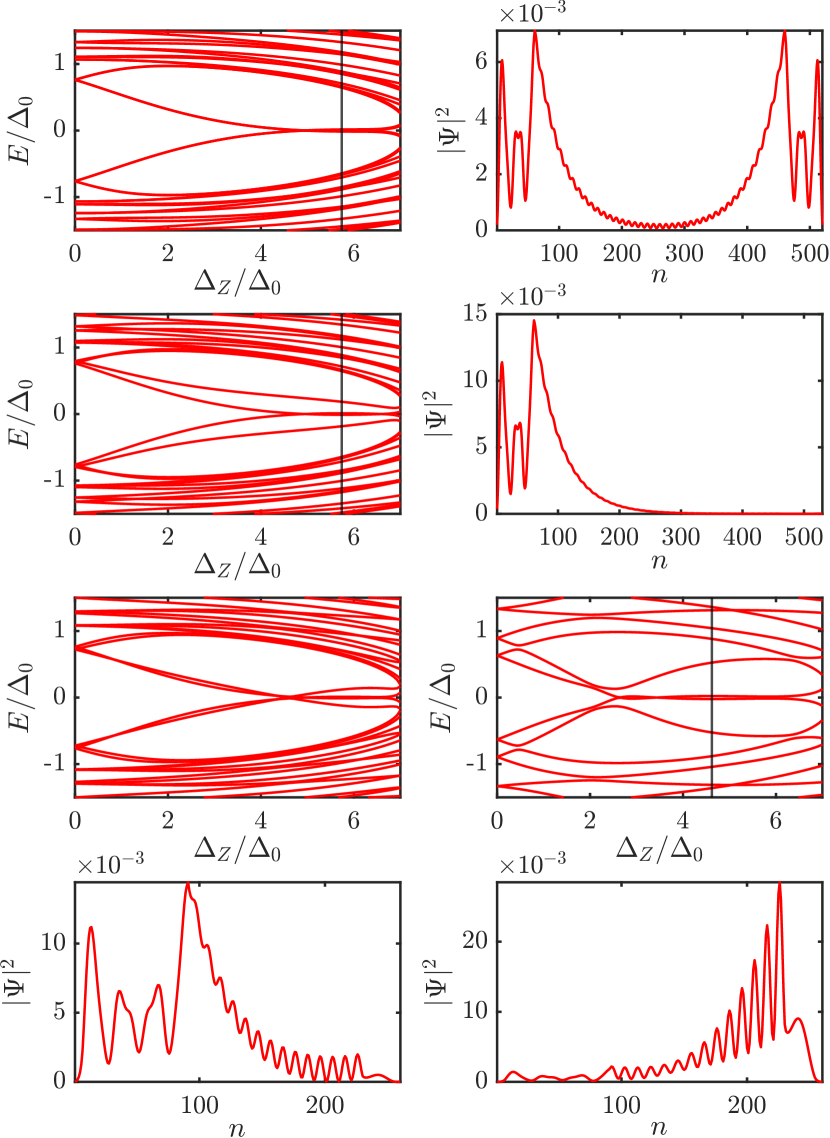
In general, a topological phase transition is accompanied by a bulk-gap closing and reopening. Here, we show that such a gap behavior can also be mimicked by two ABSs in non-topological nanowires. We tune the parameters of the right normal section away from the resonance condition by changing the length of . The degeneracy is lifted and the energy of the right ABS is different from that of the left ABS, see Fig. 6c. The parameters and do not affect the zero-energy pinning of the left ABS and can be chosen independently to control the behavior of the right ABS in dependence of the Zeeman energy. We then tune the right ABS such that it crosses the zero energy at the same value of the magnetic field at which the zero-energy pinning of the left ABS starts to take place. The resulting energy spectrum is shown in Fig. 6e and is reminiscent of what one might expect close to the topological phase transition, however, we stress that here all these features occur due to the presence of trivial ABSs in non-topological nanowires.
The nanowire examined in Fig. 6e is relatively long with a large value of the parameter , it is therefore not expected that the left ABS is visible in the local conductance on the right end of the nanowire. If instead we choose a similar parameter set as in Fig. 5, corresponding to a short nanowire and, in addition, account for a tunnel barrier (see Fig. 1b), we find the energy spectrum shown in Fig. 6f. The energy spectrum in Fig. 6f strongly resembles the gap closing and reopening one expects from a topological phase transition, but is again entirely due to ABSs. Additionally, the wavefunction of the left ABS now spreads from the left to the right end and vice versa for the wavefunction of the right ABS, see Figs. 6g and 6h.
l-0.02int0.02in(a)\stackinsetl1.7int0.02in(b)\stackinsetl-0.02int1.17in(c)\stackinsetl1.7int1.17in(d)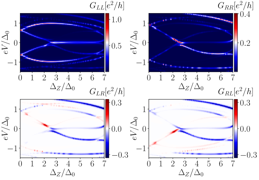
The local conductances and reveal that the ABS localized more on the left (right) is still visible at the opposite right (left) end, see Fig. 7. The left (right) ABS has a smaller conductance value on the right (left) end and the conductance is not quantized. In the absence of quantized conductances, however, this behavior significantly complicates the interpretation of future experimental data: The local conductance on the left and right end exhibits a correlated ZBP and this is accompanied by a signature reminiscent of a bulk-gap closing and reopening. In addition, the non-local conductance also exhibits the correlated left and right ABS-ZBP as well as a signature similar to a bulk-gap closing and reopening during a topological phase transition. All these features could be misinterpreted as signatures of MBSs but appear here in a nanowire that is, by design, topologically trivial at all magnetic field strengths. The complimentary scenario in short topological nanowires is discussed in App. B.
l-0.03int0.05in(a)\stackinsetl1.55int0.05in(b)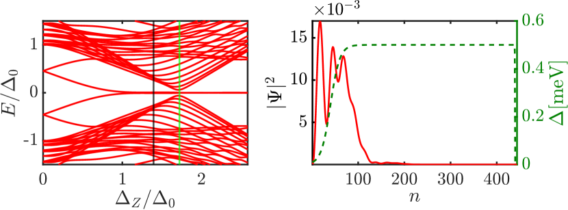
l-0.03int0.05in(c)\stackinsetl1.55int0.05in(d)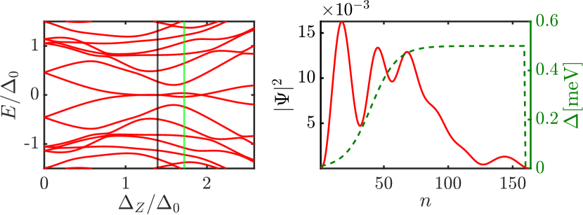
IV quasi-MBS in topological nanowires
IV.1 Quasi-MBS in the left normal section
In this section, we consider topological nanowires in configurations shown in Fig. 1a with parameter profiles shown in Fig. 2c. Such nanowires host quasi-MBSs even if the superconducting section is in the trivial phase as discussed in Sec. II.2. In Fig. 8, we compare the energy spectrum and probability density of systems with long and short superconducting sections. Quasi-MBSs at approximately zero energy exist in the trivial phase and evolve into MBSs at stronger magnetic fields. The phase transition takes place approximately at the critical value , indicated by the green line, and is accompanied by a bulk-gap closing and reopening. Changing the shape of and to step-like functions shifts quasi-MBSs to higher energies, whereas MBSs in the topological phase are not affected. The wavefunctions of the quasi-MBSs only have support on the left end of the nanowire and decay inside the superconducting section. Therefore, the probability density is only non-zero also on the right end of the nanowire when MBSs appear. The quasi-MBSs still exist in short nanowires with a small ratio and, in this case, the wavefunction spreads through the superconducting section to the right end, see Fig. 8d. In contrast to ABSs in the non-topological nanowire system considered above [see Sec. III], quasi-MBSs in a nanowire with smooth parameter profiles are more stable against fluctuations of the tunnel-barrier strength. For long wires quasi-MBSs can appear over a wide range of SOI strengths. In short nanowires, however, the quasi-MBSs are only pinned to zero for a narrow interval of the SOI strength.
l-0.00int-0.0in(a)\stackinsetl1.67int-0.0in(b)\stackinsetl-0.0int1.08in(c)\stackinsetl1.67int1.08in(d)\stackinsetl-0.0int2.16in(e)\stackinsetl1.67int2.16in(f)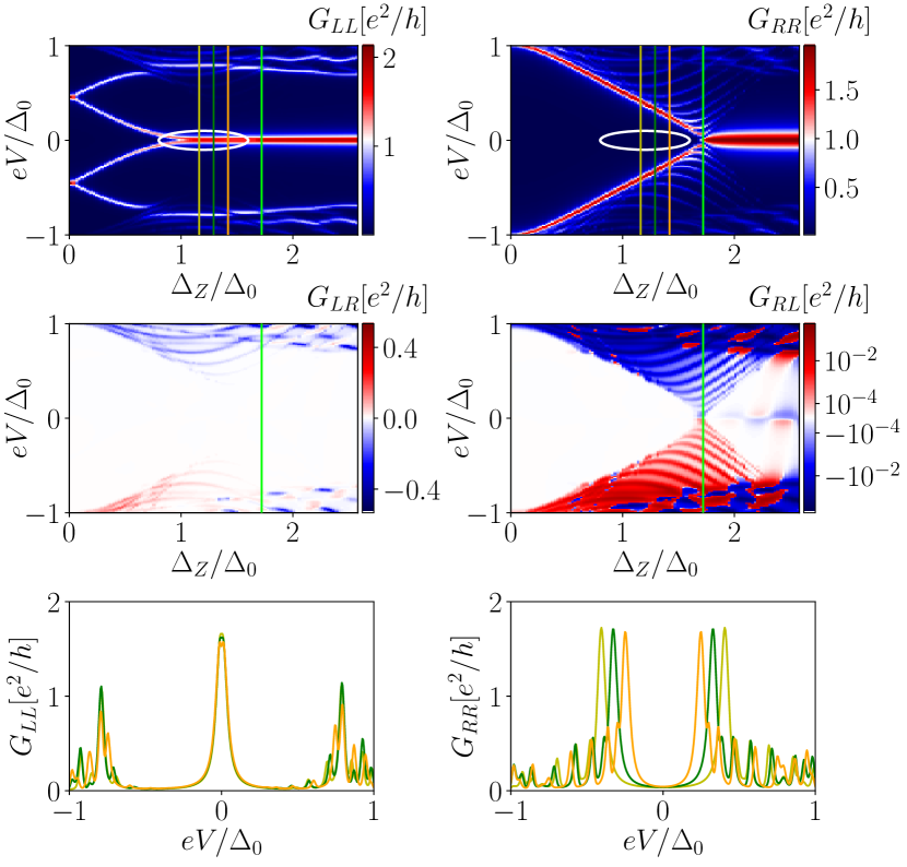
l-0.00int-0.0in(a)\stackinsetl1.67int-0.0in(b)\stackinsetl-0.0int1.08in(c)\stackinsetl1.67int1.08in(d)\stackinsetl-0.0int2.16in(e)\stackinsetl1.67int2.16in(f)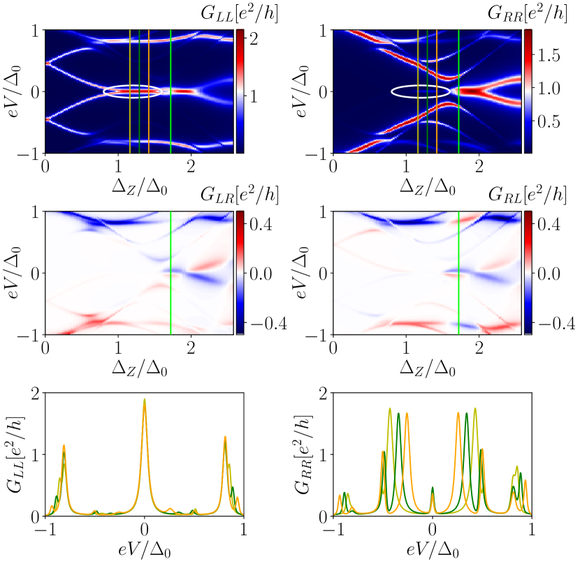
Within this setup we first study the transport properties of long topological nanowires that host quasi-MBSs, see Fig. 9. As is expected for MBSs, the conductance of these quasi-MBSs is nearly quantized to for some set of parameters, as discussed in earlier works [49]. Deviations from this value are due to line broadening effects. In long nanowires quasi-MBSs are only visible in the local conductance on the left end, , the corresponding region is encircled by an ellipse in Figs. 9a and 9b; see also Figs. 9e and 9f for line-cuts of the local conductances and at certain Zeeman energies. This behavior can be understood from the fact that the quasi-MBS wavefunction is localized on the left end of the nanowire. The bulk-gap closing and reopening is only weakly pronounced in because the bulk states are mainly localized within the superconducting section and the left lead is relative far away from this region. As a result, primarily probes the quasi-MBS (which is localized in ) but not the bulk states. It should be noted that the bulk states can become more visible using a logarithmic color scale (see Fig. 9d). The normal section on the right end is shorter and so the right local conductance is a better probe of the bulk states. The bulk-gap closing and reopening in the non-local conductances and , shown in Figs. 9c and 9d, respectively, is less clear compared to nanowires with uniform parameters as well as the quasi-MBSs and the MBSs are not visible in the non-local conductances. The right local conductance, , takes larger values close to the bulk-gap edge in the trivial regime (see Fig. 9b) since there is an ‘intrinsic’ ABS just at the gap edge, see Refs. [79, 80].
Next, we consider short superconducting sections. The conductance value of the quasi-MBS and its zero-bias pinning is essentially unaffected by the change of length, see Fig. 10. In contrast, the MBSs that occur in the topological phase are pushed away from zero energy. In short nanowires quasi-MBSs are visible in : this region is indicated by the white ellipse in Figs. 10a and 10b. The quasi-MBS-ZBP appearing in is not quantized and much smaller than that in , see also Figs. 10e and 10f for a line cut of the conductance. The right local conductance, however, exhibits a small ZBP and this peak is correlated to the one on the left end. Furthermore, while the quasi-MBSs and the MBSs generate a signal in the non-local conductances, and , the bulk-gap closing and reopening is not as clear as in the case of the long superconducting section.
IV.2 Quasi-MBSs in the left and right normal sections
l-0.00int-0.0in(a)\stackinsetl1.67int-0.0in(b)\stackinsetl-0.0int1.08in(c)\stackinsetl1.67int1.08in(d)
The final setup we consider is a topological nanowire with normal sections on both ends, see Fig. 1b, with parameter profiles specified in Fig. 2d. Such a system can host zero-energy quasi-MBSs at both ends of the nanowire in the topologically trivial regime. In App. D, we discuss the energy spectrum and the wavefunctions of bulk states, the latter is important for the understanding of the non-local conductances. The conductance patterns of the nanowire, depicted in Fig. 11, exhibit features coming from the left and right localized quasi-MBSs. As found previously, their conductance value is quantized close to . The bulk-gap closing and reopening is only weakly pronounced in the non-local conductance , although a logarithmic color scale can reveal this process, see Fig. 11d. We note that even on the logarithmic scale the bulk states are poorly visible compared to Fig. 9d, whereas the energy spectrum (dark green dashed lines) clearly shows the bulk-gap closing and reopening. This reduction of the non-local conductance signature of the bulk-gap closing and reopening by normal sections has been noted but not explained in Ref. [68]. The reason for this reduction is that the bulk states have no support in the normal sections and especially the low energy states are confined to the middle of the superconducting section and therefore these bulk states have only very weak features in the local and non-local conductances. Other states are extended throughout the whole nanowire and thus contribute more strongly to the non-local conductances, see App. B.
This suppression of the visibility of the bulk-gap closing in the non-local conductance can be somewhat offset by decreasing the step height of the chemical potential at the interface between normal and superconducting section. Nonetheless, three-terminal experiments will require a very high resolution to measure the bulk-gap closing and reopening in superconducting nanowires with normal sections on both ends. If this gap behavior cannot be resolved experimentally, then it will also not be possible to distinguish MBSs from quasi-MBSs, even in long nanowires.
V Conclusions
We analyzed transport properties of non-topological Rashba nanowires with normal sections that host ABSs. When the parameters of a normal section are close to a resonance condition and the ratio between the length of the superconductor and the ABS localization length is small, an ABS is pinned to zero energy over a wide range of Zeeman energies and has a finite probability density on both ends of the nanowire. The same effect occurs for the case of smooth spatial variation of system parameters such as chemical potential and superconducting gap. As such, even though their origin is topologically trivial, calculations of local and non-local conductances reveal correlated ZBPs on the left and the right ends of the nanowire due to the ABSs. We conclude therefore that the measurement of correlated ZBPs on both ends of a superconducting nanowire is not an unambiguous indicator for the presence of MBSs.
The observation of the closing and reopening of the bulk-gap in the local and non-local conductances that should accompany a topological phase transition has also been considered in previous works as an additional indicator for the topological phase. However, we find here that a second ABS at the other end of the nanowire can mimic the edge of the bulk-gap, when the ratio between the length of superconducting section and the localization length of the ABS is small. Therefore, local and non-local conductance measurements of ZBPs on each end with an apparent closing and reopening of the bulk-gap is also not an unambiguous indicator for the presence of MBSs.
We conclude that, while next generation three-terminal experimental devices will have access to additional auxiliary features that can help clarify the origins of ZBPs, trivial ABSs can also generate conductance features similar to those expected from MBSs when such devices do not have long superconducting sections. In particular, we find that ABSs can produce correlated ZBPs and a feature reminiscent of a bulk-gap closing and reopening in local and non-local conductances. Our results therefore suggest that it is essential to perform measurements in systems with long superconducting sections and over a large region of parameter space if one wishes to gain confidence in a purported MBS signature. That said, ballistic transport experiments favor short nanowires since presently the production of devices with long mean free paths is challenging. It is therefore questionable whether current state-of-the-art or near-term Rashba nanowire devices will be able to conclusively rule out the effects of extended ABSs. Alternatively, these three-terminal detection methods should be supplemented by additional signatures observable in the bulk [81, 82, 83, 84, 85, 86] and related to the topological phase transition, such as the inversion of spin polarization in the lowest energy bulk states [87, 88].
VI Acknowledgements
This project has received funding from the European Union’s Horizon 2020 research and innovation programme under Grant Agreement No 862046 and under Grant Agreement No 757725 (the ERC Starting Grant). This work was supported by the Georg H. Endress Foundation and the Swiss National Science Foundation.
Appendix A Energy and Transport calculation
To obtain the energy spectrum and wavefunctions, we diagonalize numerically the Hamiltonian . In addition to this we compute the differential conductance of the three-terminal device consisting of a nanowire with a grounded superconducting section and two normal leads at the left and right end using the Python package Kwant [89], which is based on the Blonder Tinkham Klapwijk (BTK) formalism [90]. In particular, we use Kwant to numerically calculate the -matrix and extract the transmission and reflection coefficients that determine the Andreev conductance matrix at zero temperature
| (17) |
where () and denote the number of channels and the gate voltage on the left (right) lead, respectively, and are the probabilities of an electron in lead to be reflected as an electron or hole, respectively, and similarly, the coefficients and are the probabilities of an electron from lead to transmit as an electron or hole to lead , respectively. The differential-conductance matrix elements [66, 91, 63] at finite temperature are given by
| (18a) | ||||
| (18b) | ||||
| (18c) | ||||
| (18d) | ||||
where denotes the Fermi distribution function , with being the Boltzmann constant. The temperature broadens peaks in the differential conductance. In this work, we perform the calculations using the temperature mK throughout, unless stated otherwise.
l-0.02int0.02in(a)\stackinsetl1.7int0.02in(b)\stackinsetl-0.02int1.17in(c)\stackinsetl1.7int1.17in(d)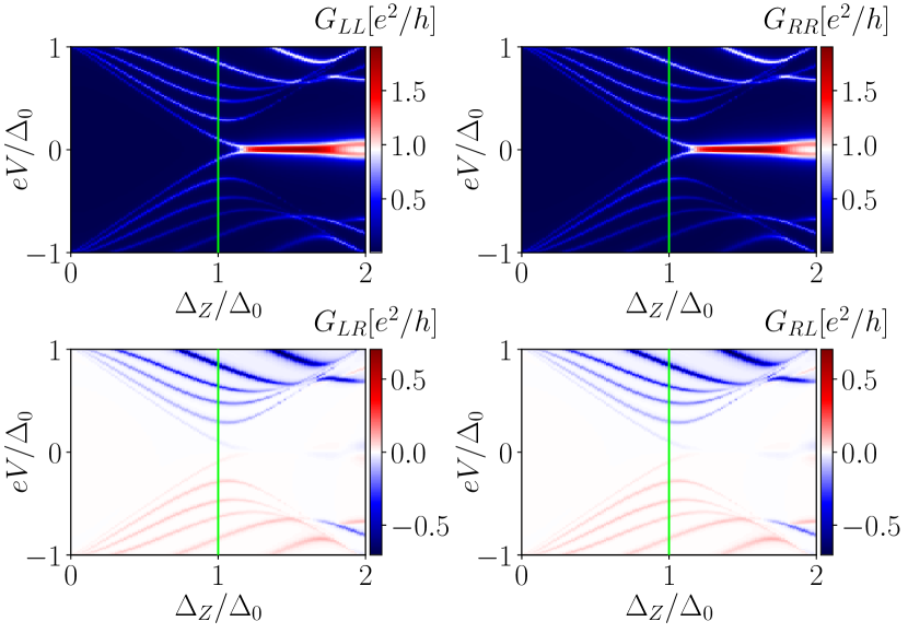
Appendix B Short uniform topological nanowire
In this section, we compute the differential conductance of a short uniform nanowire, which enters a topological phase at , see Fig. 12. This conductance behaviour is well known and is presented here in order to compare with that of a short non-topological nanowire which can exhibit similar signatures, see Fig. 7. The left and right conductance patterns exhibit features coming from the MBSs after the topological phase transition. The MBSs overlap since their localization length is comparable to the system length and therefore the non-local conductance also contains a weak MBS signature in this regime, see Figs. 12c and 12d. A logarithmic scale can, however, reveal these weak MBS signatures in the non-local conductance, for example see also Fig. 11d.
In short nanowires only a few states contribute to conductance at low biases close to the bulk-gap closing and reopening point. For instance, in the example shown in Fig. 12 only three states contribute. This should be compared to the conductance of the non-topological nanowire shown in Fig. 7, which hosts one state that mimics the bulk states undergoing a topological phase transition and is very similar to the behavior found in topological nanowires. In longer nanowires the energy level spacing between the bulk states decreases. As such, many states contribute to the conductance close to the bulk-gap closing and reopening point and therefore it is easier to distinguish between the bulk and bound states.
We note that the ZBP of the MBSs in the short topological nanowire is not quantized, which is also the case for the ZBP in the trivial nanowire. Experimentally, the robust quantization has not been observed so far. All in all, a distinction between topological and trivial states in short nanowires via a local and non-local conductance measurement is therefore challenging.
Appendix C Broadening of ZBP
We note that the calculated conductance peaks are relatively sharp. In contrast, experiments usually show broadened conductance patterns. Different mechanisms such as the strong coupling between leads and nanowire, external perturbations due to environment effects, and high temperatures lead to a broadening of the conductance peaks. In this section we consider long topological and non-topological nanowires, hosting nearly zero-energy ABSs in the left normal section, and calculate the local conductance , see Fig. 13. All broadening mechanisms are taken into account effectively via thermal effects, i.e. by choosing a relatively high temperature of mK. The resulting conductance is less sharp and is therefore in better agreement with the broader conductance features found in experiments. Furthermore, broadening prevents a high resolution mapping of the energy spectrum. The left local conductance cannot resolve the fact that the ABS has a finite energy (in Fig. 13 energies are shown as green dashed lines for comparison). The conductance peaks of the finite-energy ABS and its particle-hole partner are merged together into a single conductance peak at zero energy. As such, even in systems where ABSs are not perfectly tuned to zero energy, for example, if the resonance condition is fulfilled only approximately, an apparent ZBP in the conductance can still emerge.
l-0.02int0.02in(a)\stackinsetl1.75int0.02in(b)
Appendix D Absence of the signature of the bulk-gap closing in conductance
l0.0int0.in(a)\stackinsetl1.73int0.0in(b)\stackinsetl0.0int1.2in(c)\stackinsetl1.73int1.2in(d)
In this section we consider topological nanowires which host quasi-MBSs at both ends and analyze the suppression of signatures of the topological phase transition in the conductance. Our discussion focusses on long nanowires, for which elements of the corresponding conductance matrix is shown in Fig. 11. The non-local conductances, and , show only weak bulk-gap features at lower biases, despite the fact that the energy spectrum exhibits a clear bulk-gap closing and reopening consistent with the topological phase transition, see Fig. 14. The phase transition is indicated by the green vertical line. This puzzle can be resolved by looking at the bulk wavefunctions, see Fig. 14. The non-uniform chemical potential is responsible for confining the lowest energy bulk sub-gap states within the superconducting section. When the bulk gap closes in the superconducting section, the normal sections still nominally have a gap for states with nearly zero momentum originating from the interior branches of the spectrum. In the trivial phase (see Fig. 14b), the quasi-MBSs (blue, dark green) are well localized at the left and right ends of the nanowire. As a result, they couple strongly to the leads. In contrast, the energetically lowest bulk states (khaki green, yellow, orange and dark red) are mainly localized within the superconducting section. Thus, there is hardly any coupling to the leads and, as such, these bulk states only weakly contribute to the non-local conductance of the trivial phase.
Right after the topological phase transition (see Fig. 14c), the wavefunctions of the energetically lowest bulk states are also mainly localized within the superconducting section and not in the normal sections. This results in a similar absence of a corresponding non-local conductance signal as occurred in the trivial phase. In general, we find the lower the energy of the bulk state the more it is localized within the superconducting section. For example, the energetically lowest state (dark green) is more localized than the fifth bulk state (dark red). Furthermore, these bulk states are spatially separated from the left and right ends of the nanowire, so that a local conductance measurement also can not resolve such states. In contrast, the MBSs (dark blue) are mainly localized in the normal sections and decay into the superconductor making them highly visible in local conductance measurements.
l-0.00int-0.0in(a)\stackinsetl1.67int-0.0in(b)\stackinsetl-0.0int1.08in(c)\stackinsetl1.67int1.08in(d)\stackinsetl-0.0int2.16in(e)\stackinsetl1.67int2.16in(f)
Deep inside the topological phase (see Fig. 14d), the lowest bulk states (dark green and khaki green) originating from the exterior branches of the spectrum (from finite Fermi momentum) are extended over the entire nanowire. These delocalized states couple strongly to the leads and do contribute to the non-local conductance. In contrast, some of the energetically higher states (such as the yellow and dark red) originating from the interior branches of the spectrum (from nearly zero Fermi momentum), – which are related to the states discussed in Fig. 14c – remain confined in the superconducting section and therefore contribute less to the non-local conductance.
The absence of a clear bulk-gap closing and reopening signal in such a setup makes it essentially impossible to determine the location of the topological phase transition measuring local and non-local conductances and therefore it is also not possible to conclusively determine whether the system hosts MBSs or two quasi-MBSs. Although discussed here for long topological nanowires, this behavior also occurs in short topological nanowires.
Appendix E Interplay between quasi-MBSs at the left end and ABS at the right end of a short topological nanowire
Finally, we consider a short topological nanowire with quasi-MBSs on the left end and an ABS on the right end. The ABS is again tuned so that it mimics a bulk-gap undergoing a topological phase transition. The parameter profiles of superconducting gap and chemical potential are not identical in two normal sections. We choose a smooth parameter profile at the interface between and S, and a step-like profile at the interface between S and . The elements of the conductance matrix are shown in Fig. 15. The energy spectrum (dark green dashed lines) agrees well with features in the non-local conductance . The left quasi-MBSs leak through the superconducting section and generates a small ZBP in the right conductance , see Fig. 15b. This behavior is similar to the one of the setup shown in Fig. 10 and is again explained by the extended nature of wavefunctions. The ZBP originating from the left quasi-MBSs in the right local conductance is more pronounced in linecuts, see Fig. 15f. The energy of the right ABS decreases with increasing Zeeman energy until it is nearly zero at the same values of the magnetic field at which the quasi-MBSs begin to be pinned to zero energy (). At stronger magnetic fields (), the right ABS moves away from zero energy, mimicking the reopening of the bulk gap. The true topological phase transition, however, takes place only around . The right ABS is not only visible in but also in the non-local conductances, see Fig. 15c and 15d. Additionally this ABS generates a small feature in which is only visible in the linecut shown in Fig. 15e. We note that the height of this right ABS peak in is comparable with the one of the energetically lowest bulk state. We conclude that, in experiments, an ABS on the right end could easily mask a topological phase transition.
Appendix F Parameter values
In this section, we list all parameters used in each figure, see Table 1 and Table 2. The hyphen in the table indicates that the respective parameter was not included in the calculation: For example the nanowire considered in Fig. 4a does not include a second normal section to the right of the superconducting section. Furthermore, the asterisks indicates that the corresponding parameter runs over a finite interval which is indicated in the figure. The parameters from Figs. 4g and 4h are the same as the ones from Figs. 4a and 4e. We choose a temperature of mK in all plots except in Fig. 13, where we take mK. Furthermore, the effective lattice constant is nm in all plots. All energy values in the following tables are given in units of meV.
| Fig. | ||||||||||||||||||||||
|---|---|---|---|---|---|---|---|---|---|---|---|---|---|---|---|---|---|---|---|---|---|---|
| 3a | 60 | - | 400 | - | - | 100 | - | 20 | - | 2 | 0.25 | 1.58 | 1.75 | - | - | - | - | - | - | |||
| 3b | 60 | - | 400 | - | - | 100 | - | 20 | - | 2 | 0.25 | 1.31 | 1.75 | - | - | - | - | - | - | |||
| 3c | 60 | - | 400 | - | - | 100 | - | 20 | 0.44 | - | 2 | 0.25 | 1.75 | 13.35 | 1.78 | - | - | - | - | - | - | |
| 3d | 60 | - | 400 | - | - | 100 | - | 20 | 0.3 | - | 2 | 0.25 | 1.75 | 7.97 | 0.63 | - | - | - | - | - | - | |
| 4a | 60 | - | 400 | - | - | 100 | - | 20 | 0 | - | 2 | 0.25 | 1.75 | 14.35 | 2.06 | - | - | - | - | - | - | |
| 4c | 60 | - | 400 | - | - | 100 | - | 20 | 0 | - | 2 | 0.09 | 1.75 | 14.35 | 2.06 | - | - | - | - | - | - | |
| 4e | 60 | - | 175 | - | - | 100 | - | 20 | 0 | - | 2 | 0.25 | 1.75 | 14.35 | 2.06 | - | - | - | - | - | - | |
| 5 | 90 | 7 | 140 | 7 | 7 | 100 | 100 | 20 | 0 | 0 | 2 | 0.25 | 1.75 | 13.75 | 1.89 | 13.75 | 1.89 | 10 | 10 | 20 | 20 | |
| 6a | 60 | 60 | 400 | - | - | 100 | 100 | 20 | 0 | 0 | 2 | 0.25 | 1.75 | 14.35 | 2.06 | 14.35 | 2.06 | - | - | - | - | |
| 6c | 60 | 70 | 400 | - | - | 100 | 100 | 20 | 0 | 0 | 2 | 0.25 | 1.75 | 14.35 | 2.06 | 14.35 | 2.06 | - | - | - | - | |
| 6e | 60 | 40 | 400 | - | - | 100 | 100 | 20 | 0 | 0 | 2 | 0.25 | 1.75 | 14.35 | 2.06 | 10.33 | 1.07 | - | - | - | - | |
| 6f | 90 | 30 | 140 | 7 | 7 | 100 | 100 | 20 | 0 | 0 | 2 | 0.25 | 1.75 | 13.75 | 1.89 | 2.75 | 0.08 | 10 | 10 | - | - | |
| 7 | 90 | 30 | 140 | 7 | 7 | 100 | 100 | 20 | 0 | 0 | 2 | 0.25 | 1.75 | 13.75 | 1.89 | 2.75 | 0.08 | 10 | 10 | 20 | 20 | |
| 13b | 60 | 7 | 400 | 7 | 7 | 100 | 100 | 20 | 0.3 | 0 | 2 | 0.25 | 1.75 | 8.80 | 0.77 | 8.80 | 0.77 | 10 | 5 | 5 | 5 |
| Fig. | |||||||||||||||||||||
|---|---|---|---|---|---|---|---|---|---|---|---|---|---|---|---|---|---|---|---|---|---|
| 8a | 40 | 4 | 400 | 4 | 4 | 102 | 0.2 | 0.2 | 0.7 | 0.5 | - | 3.5 | 0.12 | 10 | 10 | - | - | 20 | - | 20 | - |
| 8c | 40 | 4 | 120 | 4 | 4 | 102 | 0.2 | 0.2 | 0.7 | 0.5 | - | 3.5 | 0.12 | 10 | 10 | - | - | 20 | - | 20 | - |
| 9 | 40 | 4 | 400 | 4 | 4 | 102 | 0.2 | 0.2 | 0.7 | 0.5 | - | 3.5 | 0.12 | 10 | 10 | 20 | 20 | 20 | - | 20 | - |
| 10 | 40 | 4 | 120 | 4 | 4 | 102 | 0.2 | 0.2 | 0.7 | 0.5 | - | 3.5 | 0.12 | 10 | 10 | 20 | 20 | 20 | - | 20 | - |
| 11 | 40 | 48 | 400 | 4 | 4 | 102 | 0.2 | 0.1 | 0.7 | 0.5 | - | 3.5 | 0.12 | 10 | 10 | 20 | 20 | 20 | 24 | 20 | 24 |
| 12 | 4 | 4 | 140 | 4 | 4 | 102 | 0 | 0 | 0 | 0.7 | - | 3.5 | 0.12 | 10 | 10 | 20 | 20 | - | - | - | - |
| 13a | 40 | 4 | 400 | 4 | 4 | 102 | 0.2 | 0.2 | 0.7 | 0.5 | - | 3.5 | 0.12 | 10 | 10 | 20 | 20 | 10 | - | 20 | - |
| 14 | 40 | 48 | 400 | 4 | 4 | 102 | 0.2 | 0.1 | 0.7 | 0.5 | - | 3.5 | 0.12 | 10 | 10 | - | - | 20 | 24 | 20 | 24 |
| 15 | 40 | 32 | 120 | 4 | 4 | 102 | 0.2 | 0.2 | 0.7 | 0.5 | - | 3.5 | 0.12 | 10 | 10 | 20 | 20 | 20 | - | 20 | - |
References
- Kitaev [2001] A. Y. Kitaev, Phys. Usp. 44, 131 (2001).
- Fujimoto [2008] S. Fujimoto, Phys. Rev. B 77, 220501 (2008).
- Sato et al. [2009] M. Sato, Y. Takahashi, and S. Fujimoto, Phys. Rev. Lett. 103, 020401 (2009).
- Volovik [2009] G. Volovik, JETP Lett. 90, 398 (2009).
- Oreg et al. [2010] Y. Oreg, G. Refael, and F. von Oppen, Phys. Rev. Lett. 105, 177002 (2010).
- Lutchyn et al. [2010] R. M. Lutchyn, J. D. Sau, and S. Das Sarma, Phys. Rev. Lett. 105, 077001 (2010).
- Sato et al. [2010] M. Sato, Y. Takahashi, and S. Fujimoto, Phys. Rev. B 82, 134521 (2010).
- Moore and Read [1991] G. Moore and N. Read, Nucl. Phys. B 360, 362 (1991).
- Volovik [1999] G. Volovik, JETP Lett. 70, 609 (1999).
- Read and Green [2000] N. Read and D. Green, Phys. Rev. B 61, 10267 (2000).
- Senthil and Fisher [2000] T. Senthil and M. P. A. Fisher, Phys. Rev. B 61, 9690 (2000).
- Ivanov [2001] D. A. Ivanov, Phys. Rev. Lett. 86, 268 (2001).
- Nayak et al. [2008] C. Nayak, S. H. Simon, A. Stern, M. Freedman, and S. Das Sarma, Rev. Mod. Phys. 80, 1083 (2008).
- Alicea [2012] J. Alicea, Rep. Prog. Phys. 75, 076501 (2012).
- Beenakker [2013] C. Beenakker, Annu. Rev. Condens. Matter Phys. 4, 113 (2013).
- Law et al. [2009] K. T. Law, P. A. Lee, and T. K. Ng, Phys. Rev. Lett. 103, 237001 (2009).
- Akhmerov et al. [2009] A. R. Akhmerov, J. Nilsson, and C. W. J. Beenakker, Phys. Rev. Lett. 102, 216404 (2009).
- Flensberg [2010] K. Flensberg, Phys. Rev. B 82, 180516 (2010).
- Wimmer et al. [2011] M. Wimmer, A. R. Akhmerov, J. P. Dahlhaus, and C. W. J. Beenakker, New J. Phys. 13, 053016 (2011).
- Chevallier and Klinovaja [2016] D. Chevallier and J. Klinovaja, Phys. Rev. B 94, 035417 (2016).
- Prada et al. [2012] E. Prada, P. San-Jose, and R. Aguado, Phys. Rev. B 86, 180503 (2012).
- Das Sarma et al. [2012] S. Das Sarma, J. D. Sau, and T. D. Stanescu, Phys. Rev. B 86, 220506 (2012).
- Rainis et al. [2013] D. Rainis, L. Trifunovic, J. Klinovaja, and D. Loss, Phys. Rev. B 87, 024515 (2013).
- Dmytruk and Klinovaja [2018] O. Dmytruk and J. Klinovaja, Phys. Rev. B 97, 155409 (2018).
- Fleckenstein et al. [2018] C. Fleckenstein, F. Domínguez, N. Traverso Ziani, and B. Trauzettel, Phys. Rev. B 97, 155425 (2018).
- Sasaki et al. [2011] S. Sasaki, M. Kriener, K. Segawa, K. Yada, Y. Tanaka, M. Sato, and Y. Ando, Phys. Rev. Lett. 107, 217001 (2011).
- Mourik et al. [2012] V. Mourik, K. Zuo, S. M. Frolov, S. R. Plissard, E. P. A. M. Bakkers, and L. P. Kouwenhoven, Science 336, 1003 (2012).
- Deng et al. [2012] M. T. Deng, C. L. Yu, G. Y. Huang, M. Larsson, P. Caroff, and H. Q. Xu, Nano Lett. 12, 6412 (2012).
- Das et al. [2012] A. Das, Y. Ronen, Y. Most, Y. Oreg, M. Heiblum, and H. Shtrikman, Nat. Phys. 8, 887 (2012).
- Churchill et al. [2013] H. O. H. Churchill, V. Fatemi, K. Grove-Rasmussen, M. T. Deng, P. Caroff, H. Q. Xu, and C. M. Marcus, Phys. Rev. B 87, 241401 (2013).
- Albrecht et al. [2016] S. M. Albrecht, A. P. Higginbotham, M. Madsen, F. Kuemmeth, T. S. Jespersen, J. Nygård, P. Krogstrup, and C. M. Marcus, Nature 531, 206 (2016).
- Schneider et al. [2021] L. Schneider, P. Beck, J. Neuhaus-Steinmetz, T. Posske, J. Wiebe, and R. Wiesendanger, (2021), arXiv:2104.11503 .
- Rosdahl et al. [2018] T. O. Rosdahl, A. Vuik, M. Kjaergaard, and A. R. Akhmerov, Phys. Rev. B 97, 045421 (2018).
- Pikulin et al. [2021] D. I. Pikulin, B. van Heck, T. Karzig, E. A. Martinez, B. Nijholt, T. Laeven, G. W. Winkler, J. D. Watson, S. Heedt, M. Temurhan, V. Svidenko, R. M. Lutchyn, M. Thomas, G. de Lange, L. Casparis, and C. Nayak, (2021), arXiv:2103.12217 .
- de Gennes and Saint-James [1963] P. de Gennes and D. Saint-James, Phys. Lett. 4, 151 (1963).
- Andreev [1964] A. F. Andreev, Sov. Phys. JETP 19, 1228 (1964).
- Caroli et al. [1964] C. Caroli, P. De Gennes, and J. Matricon, Phys. Lett. 9, 307 (1964).
- Andreev [1966] A. F. Andreev, Sov. Phys. JETP 22, 455 (1966).
- Shiba [1968] H. Shiba, Prog. Theor. Phys. 40, 435 (1968).
- A.I.Rusinov [1969] A.I.Rusinov, Sov. Phys. JETP 29, 1101 (1969).
- Sauls [2018] J. A. Sauls, Phil. Trans. R. Soc. 376 (2018).
- Prada et al. [2020] E. Prada, P. San-Jose, M. W. A. de Moor, A. Geresdi, E. J. H. Lee, J. Klinovaja, D. Loss, J. Nygård, R. Aguado, and L. P. Kouwenhoven, Nat. Rev. Phys. 2, 575 (2020).
- Kells et al. [2012] G. Kells, D. Meidan, and P. W. Brouwer, Phys. Rev. B 86, 100503 (2012).
- Lee et al. [2012] E. J. H. Lee, X. Jiang, R. Aguado, G. Katsaros, C. M. Lieber, and S. De Franceschi, Phys. Rev. Lett. 109, 186802 (2012).
- Cayao et al. [2015] J. Cayao, E. Prada, P. San-Jose, and R. Aguado, Phys. Rev. B 91, 024514 (2015).
- Ptok et al. [2017] A. Ptok, A. Kobiałka, and T. Domański, Phys. Rev. B 96, 195430 (2017).
- Liu et al. [2017] C.-X. Liu, J. D. Sau, T. D. Stanescu, and S. Das Sarma, Phys. Rev. B 96, 075161 (2017).
- Reeg et al. [2018a] C. Reeg, O. Dmytruk, D. Chevallier, D. Loss, and J. Klinovaja, Phys. Rev. B 98, 245407 (2018a).
- Peñaranda et al. [2018] F. Peñaranda, R. Aguado, P. San-Jose, and E. Prada, Phys. Rev. B 98, 235406 (2018).
- Moore et al. [2018] C. Moore, T. D. Stanescu, and S. Tewari, Phys. Rev. B 97, 165302 (2018).
- Vuik et al. [2019] A. Vuik, B. Nijholt, A. R. Akhmerov, and M. Wimmer, SciPost Phys. 7, 61 (2019).
- Woods et al. [2019a] B. D. Woods, J. Chen, S. M. Frolov, and T. D. Stanescu, Phys. Rev. B 100, 125407 (2019a).
- Liu et al. [2019] C.-X. Liu, J. D. Sau, T. D. Stanescu, and S. Das Sarma, Phys. Rev. B 99, 024510 (2019).
- Chen et al. [2019] J. Chen, B. D. Woods, P. Yu, M. Hocevar, D. Car, S. R. Plissard, E. P. A. M. Bakkers, T. D. Stanescu, and S. M. Frolov, Phys. Rev. Lett. 123, 107703 (2019).
- Alspaugh et al. [2020] D. J. Alspaugh, D. E. Sheehy, M. O. Goerbig, and P. Simon, Phys. Rev. Research 2, 023146 (2020).
- Jünger et al. [2020] C. Jünger, R. Delagrange, D. Chevallier, S. Lehmann, K. A. Dick, C. Thelander, J. Klinovaja, D. Loss, A. Baumgartner, and C. Schönenberger, Phys. Rev. Lett. 125, 017701 (2020).
- Valentini et al. [2020] M. Valentini, F. Peñaranda, A. Hofmann, M. Brauns, R. Hauschild, P. Krogstrup, P. San-Jose, E. Prada, R. Aguado, and G. Katsaros, (2020), arXiv:2008.02348 .
- O’Farrell et al. [2018] E. C. T. O’Farrell, A. C. C. Drachmann, M. Hell, A. Fornieri, A. M. Whiticar, E. B. Hansen, S. Gronin, G. C. Gardner, C. Thomas, M. J. Manfra, K. Flensberg, C. M. Marcus, and F. Nichele, Phys. Rev. Lett. 121, 256803 (2018).
- Shen et al. [2018] J. Shen, S. Heedt, F. Borsoi, B. van Heck, S. Gazibegovic, R. L. M. Op het Veld, D. Car, J. A. Logan, M. Pendharkar, S. J. J. Ramakers, G. Wang, D. Xu, D. Bouman, A. Geresdi, C. J. Palmstrøm, E. P. A. M. Bakkers, and L. P. Kouwenhoven, Nat. Com. 9, 4801 (2018).
- Cao et al. [2019] Z. Cao, H. Zhang, H.-F. Lü, W.-X. He, H.-Z. Lu, and X. C. Xie, Phys. Rev. Lett. 122, 147701 (2019).
- Pan et al. [2020] H. Pan, W. S. Cole, J. D. Sau, and S. Das Sarma, Phys. Rev. B 101, 024506 (2020).
- Entin-Wohlman et al. [2008] O. Entin-Wohlman, Y. Imry, and A. Aharony, Phys. Rev. B 78, 224510 (2008).
- Lobos and Sarma [2015] A. M. Lobos and S. D. Sarma, New J. Phys. 17, 065010 (2015).
- Gramich et al. [2017] J. Gramich, A. Baumgartner, and C. Schönenberger, Phys. Rev. B 96, 195418 (2017).
- Zhang et al. [2019] H. Zhang, D. E. Liu, M. Wimmer, and L. P. Kouwenhoven, Nat. Com. 10, 5128 (2019).
- Danon et al. [2020] J. Danon, A. B. Hellenes, E. B. Hansen, L. Casparis, A. P. Higginbotham, and K. Flensberg, Phys. Rev. Lett. 124, 036801 (2020).
- Melo et al. [2021] A. Melo, C.-X. Liu, P. Rożek, T. Örn Rosdahl, and M. Wimmer, SciPost Phys. 10, 37 (2021).
- Pan et al. [2021] H. Pan, J. D. Sau, and S. Das Sarma, Phys. Rev. B 103, 014513 (2021).
- Ménard et al. [2020] G. C. Ménard, G. L. R. Anselmetti, E. A. Martinez, D. Puglia, F. K. Malinowski, J. S. Lee, S. Choi, M. Pendharkar, C. J. Palmstrøm, K. Flensberg, C. M. Marcus, L. Casparis, and A. P. Higginbotham, Phys. Rev. Lett. 124, 036802 (2020).
- Puglia et al. [2020] D. Puglia, E. A. Martinez, G. C. Ménard, A. Pöschl, S. Gronin, G. C. Gardner, R. Kallaher, M. J. Manfra, C. M. Marcus, A. P. Higginbotham, and L. Casparis, (2020), arXiv:2006.01275 .
- Yu et al. [2021] P. Yu, J. Chen, M. Gomanko, G. Badawy, E. P. A. M. Bakkers, K. Zuo, V. Mourik, and S. M. Frolov, Nat. Phys. 17, 482 (2021).
- Reeg et al. [2017] C. Reeg, D. Loss, and J. Klinovaja, Phys. Rev. B 96, 125426 (2017).
- Reeg et al. [2018b] C. Reeg, D. Loss, and J. Klinovaja, Phys. Rev. B 97, 165425 (2018b).
- Reeg et al. [2018c] C. Reeg, D. Loss, and J. Klinovaja, Beilstein J. Nanotechnol 9, 1263 (2018c).
- Woods et al. [2019b] B. D. Woods, S. Das Sarma, and T. D. Stanescu, Phys. Rev. B 99, 161118 (2019b).
- Winkler et al. [2019] G. W. Winkler, A. E. Antipov, B. van Heck, A. A. Soluyanov, L. I. Glazman, M. Wimmer, and R. M. Lutchyn, Phys. Rev. B 99, 245408 (2019).
- Kiendl et al. [2019] T. Kiendl, F. von Oppen, and P. W. Brouwer, Phys. Rev. B 100, 035426 (2019).
- Klinovaja and Loss [2015] J. Klinovaja and D. Loss, Eur. Phys. J. B 88, 62 (2015).
- Huang et al. [2018] Y. Huang, H. Pan, C.-X. Liu, J. D. Sau, T. D. Stanescu, and S. Das Sarma, Phys. Rev. B 98, 144511 (2018).
- Aseev et al. [2018] P. P. Aseev, J. Klinovaja, and D. Loss, Phys. Rev. B 98, 155414 (2018).
- Gulden et al. [2016] T. Gulden, M. Janas, Y. Wang, and A. Kamenev, Phys. Rev. Lett. 116, 026402 (2016).
- Serina et al. [2018] M. Serina, D. Loss, and J. Klinovaja, Phys. Rev. B 98, 035419 (2018).
- Yang et al. [2019] F. Yang, S.-J. Jiang, and F. Zhou, Phys. Rev. B 100, 054508 (2019).
- Tamura et al. [2019] S. Tamura, S. Hoshino, and Y. Tanaka, Phys. Rev. B 99, 184512 (2019).
- Sticlet et al. [2020] D. Sticlet, C. P. Moca, and B. Dóra, Phys. Rev. B 102, 075437 (2020).
- Mashkoori et al. [2020] M. Mashkoori, S. Pradhan, K. Björnson, J. Fransson, and A. M. Black-Schaffer, Phys. Rev. B 102, 104501 (2020).
- Szumniak et al. [2017] P. Szumniak, D. Chevallier, D. Loss, and J. Klinovaja, Phys. Rev. B 96, 041401 (2017).
- Chevallier et al. [2018] D. Chevallier, P. Szumniak, S. Hoffman, D. Loss, and J. Klinovaja, Phys. Rev. B 97, 045404 (2018).
- Groth et al. [2014] C. W. Groth, M. Wimmer, A. R. Akhmerov, and X. Waintal, New J. Phys. 16, 063065 (2014).
- Blonder et al. [1982] G. E. Blonder, M. Tinkham, and T. M. Klapwijk, Phys. Rev. B 25, 4515 (1982).
- Fregoso et al. [2013] B. M. Fregoso, A. M. Lobos, and S. Das Sarma, Phys. Rev. B 88, 180507 (2013).