Broadband Focusing of Acoustic Plasmons in Graphene with an Applied Current
Abstract
Non-reciprocal plasmons in current-driven, isotropic, and homogenous graphene with proximal metallic gates is theoretically explored. Nearby metallic gates screen the Coulomb interactions, leading to linearly dispersive acoustic plasmons residing close to its particle-hole continuum counterpart. We show that the applied bias leads to spectral broadband focused plasmons whose resonance linewidth is dependent on the angular direction relative to the current flow due to Landau damping. We predict that forward focused non-reciprocal plasmons are possible with accessible experimental parameters and setup.
As optoelectronic technology advances, there is increasing demand for the development of strongly non-reciprocal light based devices. [1, 2, 3, 4] While magneto-optical systems are well known for exhibiting non-reciprocity, the need for an external magnetic bias makes it difficult to integrate these systems onto nanophotonic platforms. This has driven a shift of the focus in recent years to the use of an external current bias to induce non-reciprocity.[5, 6, 7, 8, 9, 10, 11, 12] Particular focus has been given to graphene surface plasmons, as their wide frequency range and gate tunability offer a wide variety of applications.[13, 14, 15, 16, 17, 18, 19]
The effect of a current bias on graphene surface plasmons is to induce a Doppler shift in the plasmonic spectrum. By this effect, plasmons that are moving in the same direction as the electron flow are blue-shifted, while plasmons moving against the electron flow are red-shifted.[9] It has been shown that when the drift velocity is a significant fraction of the Fermi velocity in graphene, there exists a band of frequencies in which the red-shifted plasmons are forbidden and the plasmon is effectively unidirectional.[9, 5, 6]
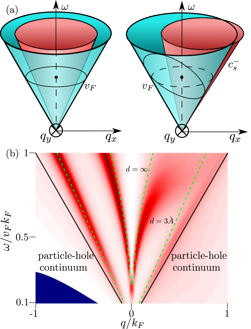
In this Letter, we show that a more versatile phenomenon can be found in graphene-dielectric-metal systems which exhibit acoustic plasmons.[20, 21, 22, 23] When the separation between the metal and graphene is small, the sound velocity of the acoustic plasmon is within a few percent of the Fermi velocity; and the plasmon branch lies in close proximity to the particle-hole continuum.[15, 24, 25, 26] If in addition an external bias is applied to the system, the plasmons moving against the electron flow can be brought into the particle-hole continuum and become damped. This focuses the acoustic plasmons in the direction of the electron flow. Below we provide analytical and numerical calculations which show how the focusing effect depends on the applied current, the electron density, and the dielectric environment. We emphasize that the major advantage in this system compared to the conventional plasmons is that the focusing effect occurs at all frequencies. Hence, it is more suitable for broadband applications.
Within the random phase approximation (RPA), the dynamical polarization of graphene is given by[14, 13]
| (1) | |||
| (2) |
where is the spin(valley) degeneracy, the prefactor is the band-overlap integral, and is the dispersion of the conduction and valence band . We assume that the graphene is isotropic and spatially homogenous. Within the Dirac-cone approximation, we have with cm s-1, and
| (3) |
where is the angle between the wave vector ( or ) and the -axis. The equilibrium electronic occupation is determined by the Fermi-Dirac distribution
| (4) |
where is the Fermi energy measured relative to the charge neutrality point, and is the temperature of the system. We assume for definiteness that .
In the presence of an applied current, the electrons reach a new quasi-equilibrium with a modified distribution function . The modified Dirac distribution can be modelled by shifting the Fermi surface of the biased electrons by an amount , where is the current density, is the conductivity in graphene, and is the transport scattering time.[8, 9] Assuming that the current is in the positive -direction, the Fermi wave number obtains an angular dependence described by
| (5) |
where we assume and . An illustration of the shifted Fermi surface is shown in Fig. 1(a). Assuming that the Fermi surface is shifted in the positive -direction, we see that the shifted Fermi surface depletes the electron concentration in the direction of the current and increases their concentration in the opposite direction. As we argue below, this shift of the Drude weight is responsible for the red-shift of the dispersion in the direction of the current.
The plasmon dispersion is determined by solving the equation
| (6) |
where
| (7) |
is the Coulomb interaction of the graphene-dielectric-metal system, is the dielectric constant of the system, and is the thickness of the dielectric layer, and we have used the approximation . In order to obtain analytical results, we consider the limit , and . In this limit, the band overlap integral simplifies to , allowing us to focus only on the intraband contribution. As we show in the Supplemental material, for along the -direction takes a surprisingly simple form,
| (8) | |||
| (9) | |||
| (10) | |||
| (11) |
where , and is the density of states in graphene. In Eq. (8) we have included terms up to second order in . Thus we find the acoustic plasmon dispersion by substituting Eqs. (8)-(11) into Eq. (6). Expanding we find
| (12) | |||
| (13) | |||
| (14) |
where , and we have used Eq. (7) in the limit of small .
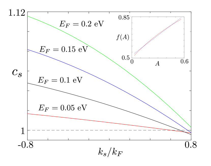
Let us discuss the dispersion defined by Eqs. (12)-(14), which is plotted in Fig. 2. As we see from Eq. (13), the dependence on creates a non-reciprocity between the and branches. As the current increases, the plasmon branch is red-shifted (blue-shifted) relative to the zero current value defined in Eq. (12). This effect creates a particularly interesting situation for acoustic plasmons in graphene, as it suggests that there is some above which . Under this condition, the plasmon branch lies entirely in the Landau damping region and is strongly damped, while the branch is very weakly attenuated (see Fig. 1 (a)). In this regime the plasmon is focused in the opposite direction of the applied bias. We can solve for using Eqs. (12)-(14) and define
| (15) |
where is a dimensionless function that monotonically increases with the parameter . This function is shown as the inset of Fig. (2) for and ranging from 0.01-0.2 eV.
Eq. (15) has some important experimental implications. The wave number defines a critical current
| (16) |
in which the acoustic plasmon focusing occurs. Here is the electron density. By consideration of , Eq. (16) suggests that can be tuned by either changing the density with an external gate, or changing the dielectric environment of the sample. As an example, let us consider what this means for hBN encapsulated graphene which has some of the highest saturation currents measured in graphene. For an electron density of cm-2 and the dielectric constant ,[27] the critical current density is approximately 800 A/m. This suggests that the focusing of the acoustic plasmon can be observed at these densities.[28]
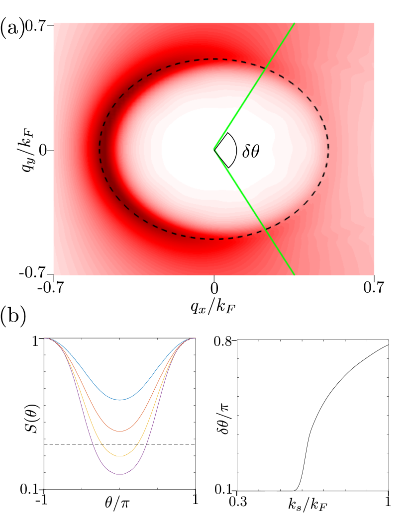
Let us now compare these results to those obtained by a numerical calculation of the polarization defined by Eq. (1). In Fig. 3(a) we present a slice of the loss function at a fixed frequency for meV and for . Here we use the polar coordinates and for describing features of , and drop from the argument for simplicity of notation. The particle-hole continuum is illustrated by the dashed black circle. There are several essential features to notice. First, let us define the isofrequency contour as the maximum of at a fixed . Unlike the zero bias case, it is clear that the isofrequency contour has shifted due to the bias, and is no longer circularly symmetric. More importantly, a range of angles around has crossed into the particle-hole continuum. The spectral intensity of this region has been nearly fully depleted. In order to investigate this more thoroughly, we plot the isofrequency contour in the left plot of Fig. 3(b) . The values are normalized to the maximum value of for each value of separately. We see that as the current bias is increased, the minimum of decreases and the size of the depleted region grows, suggesting that as the bias is increased the acoustic plasmon becomes more focused in the direction opposing the current. This allows us to define a measure of the focusing by the range of angles in which the loss function , where is Euler’s constant and is presented in the right plot of Fig. 3(b). By this criterion, the acoustic plasmon focusing does not occur until a minimum value of is applied at this Fermi energy.
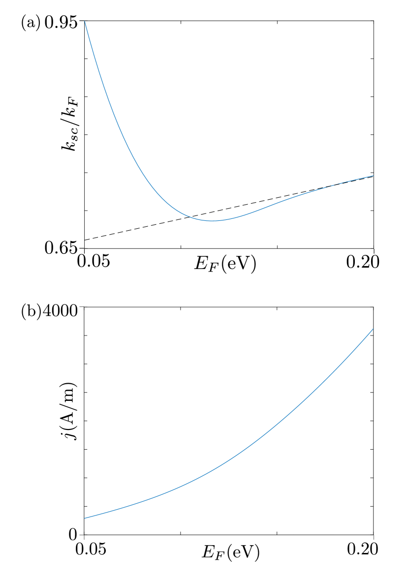
Let us discuss how these results can be tuned with the (unbiased) Fermi energy. From the angular dependence of the loss function, we can define a critical value above which the angle of depletion . In Fig. 4 we plot vs based on this criterion, along with the associated current obtained from Eq. (16). At larger , there is an approximately linear dependence of on the Fermi energy , with (eV)-1 and , as shown by the dashed line in Fig 4(a). This should be compared with our original analytical calculation in which (eV)-1 and . We note that our analytical expression dramatically overestimates the slope. This is likely due to the difference in definition of between the analytical and numerical calculations. The analytical calculation is determined by the plasmon dispersion along the -axis, which is most sensitive to the applied bias and thus more sensitive to changes in the Fermi energy and system parameters. At smaller Fermi energies, there is a sudden increase in the value of . This is likely due to the large intrinsic broadening of the plasmon peak of at smaller Fermi energies. As the Fermi energy is decreased, the plasmon peak at zero bias is pushed closer to the particle hole continuum, eventually having a partial overlap due to the finite width of the plasmon peak. As the focusing effect is caused by the red-shift of the plasmon dispersion into the particle-hole continuum with a finite bias, this partial overlap at zero bias weakens the effect.[29]
We briefly comment on the effects of disorder on these results. For hard scattering centers, the large momentum transfer makes it possible to couple opposing plasmon modes. It is reasonable to worry that this coupling would cause significant damping of the blue-shifted branch, destroying the focusing effect. However, it has been shown in previous studies that the main impact of disorder scattering on the plasmon damping factor is through the coupling of the plasmon to the particle hole continuum.[30, 31] For moderate disorder this increases the damping by roughly a factor of 2 and weakens the proposed effect. However, with the unprecedented advancement in high quality graphene heterostructure fabrication, experimental realization of our predictions in high quality factor plasmon in graphene should be within reach.
Before concluding, let us briefly dwell on the region of Fig. 1(b) in which there is gain, i.e. the region of negative loss. As we show in Fig. 1(a), the applied bias causes a population inversion in which there is a concentration of higher energy electrons in the direction opposing the current, and lower energy empty states in the direction of the current. The driving of the particles from the high energy occupied states into the lower energy states results in an energy gain in the system, and has been studied previously in optically pumped systems.[32] In the systems being studied here, this effect is limited to large wave numbers and low frequencies, limiting its potential use.[29]
To summarize, we have studied the effects of an applied current bias on acoustic plasmons in metal-dielectric-graphene systems. We have shown that for thin dielectric layers, the applied current bias focuses the acoustic plasmons in the direction opposite to the current bias. This focusing effect can be enhanced by depleting the electron concentration, or by using a material with a higher dielectric constant. We emphasize that due the linear dispersion of the acoustic plasmons, the focusing effect is spectrally broad, making it ideal for development of nonreciprocal light based devices.
Acknowledgment M.S, E.M. and T.L. acknowledge support from the National Science Foundation under Grant No. NSF/EFRI-1741660. D.M. acknowledges partial support by the ARO MURI Award No. W911NF-14-1-0247.
References
- Koenderink et al. [2015] A. F. Koenderink, A. Alu, and A. Polman, Science 348, 516 (2015).
- Lira et al. [2012] H. Lira, Z. Yu, S. Fan, and M. Lipson, Physical review letters 109, 033901 (2012).
- Fan et al. [2012] L. Fan, J. Wang, L. T. Varghese, H. Shen, B. Niu, Y. Xuan, A. M. Weiner, and M. Qi, Science 335, 447 (2012).
- Sounas et al. [2013] D. L. Sounas, C. Caloz, and A. Alu, Nature communications 4, 2407 (2013).
- Morgado and Silveirinha [2018] T. A. Morgado and M. G. Silveirinha, ACS Photonics 5, 4253 (2018), https://doi.org/10.1021/acsphotonics.8b00987 .
- Morgado and Silveirinha [2020] T. A. Morgado and M. G. Silveirinha, Physical Review B 102, 075102 (2020).
- Bliokh et al. [2018] K. Bliokh, F. J. Rodríguez-Fortuño, A. Bekshaev, Y. Kivshar, and F. Nori, Optics letters 43, 963 (2018).
- Sabbaghi et al. [2015] M. Sabbaghi, H.-W. Lee, T. Stauber, and K. S. Kim, Phys. Rev. B 92, 195429 (2015).
- Borgnia et al. [2015] D. S. Borgnia, T. V. Phan, and L. S. Levitov, arXiv preprint arXiv:1512.09044 (2015).
- Gao et al. [2019] H. Gao, Z. Dong, and L. Levitov, arXiv preprint arXiv:1912.13409 (2019).
- Dyakonov and Shur [1993] M. Dyakonov and M. Shur, Physical review letters 71, 2465 (1993).
- Van Duppen et al. [2016] B. Van Duppen, A. Tomadin, A. N. Grigorenko, and M. Polini, 2D Materials 3, 015011 (2016).
- Hwang and Das Sarma [2007] E. H. Hwang and S. Das Sarma, Phys. Rev. B 75, 205418 (2007).
- Stauber [2014] T. Stauber, Journal of Physics: Condensed Matter 26, 123201 (2014).
- Principi et al. [2011] A. Principi, R. Asgari, and M. Polini, Solid State Communications 151, 1627 (2011).
- Low and Avouris [2014] T. Low and P. Avouris, ACS nano 8, 1086 (2014).
- Wunsch et al. [2006] B. Wunsch, T. Stauber, F. Sols, and F. Guinea, New Journal of Physics 8, 318 (2006).
- Fei et al. [2012] Z. Fei, A. Rodin, G. O. Andreev, W. Bao, A. McLeod, M. Wagner, L. Zhang, Z. Zhao, M. Thiemens, G. Dominguez, et al., Nature 487, 82 (2012).
- Chen et al. [2012] J. Chen, M. Badioli, P. Alonso-González, S. Thongrattanasiri, F. Huth, J. Osmond, M. Spasenović, A. Centeno, A. Pesquera, P. Godignon, et al., Nature 487, 77 (2012).
- Lee et al. [2019] I.-H. Lee, D. Yoo, P. Avouris, T. Low, and S.-H. Oh, Nature nanotechnology 14, 313 (2019).
- Alonso-González et al. [2017] P. Alonso-González, A. Y. Nikitin, Y. Gao, A. Woessner, M. B. Lundeberg, A. Principi, N. Forcellini, W. Yan, S. Vélez, A. J. Huber, et al., Nature nanotechnology 12, 31 (2017).
- Lundeberg et al. [2017] M. B. Lundeberg, Y. Gao, R. Asgari, C. Tan, B. Van Duppen, M. Autore, P. Alonso-González, A. Woessner, K. Watanabe, T. Taniguchi, et al., Science 357, 187 (2017).
- Menabde et al. [2021] S. G. Menabde, I.-H. Lee, S. Lee, H. Ha, J. T. Heiden, D. Yoo, T.-T. Kim, T. Low, Y. H. Lee, S.-H. Oh, and M. S. Jang, Nature communications 12, 938 (2021).
- Stauber and Gómez-Santos [2012] T. Stauber and G. Gómez-Santos, New Journal of Physics 14, 105018 (2012).
- Hwang and Das Sarma [2009] E. H. Hwang and S. Das Sarma, Phys. Rev. B 80, 205405 (2009).
- Voronin et al. [2020] K. V. Voronin, U. A. Aguirreche, R. Hillenbrand, V. S. Volkov, P. Alonso-González, and A. Y. Nikitin, Nanophotonics 1 (2020).
- Laturia et al. [2018] A. Laturia, M. L. Van de Put, and W. G. Vandenberghe, npj 2D Materials and Applications 2, 1 (2018).
- Yamoah et al. [2017] M. A. Yamoah, W. Yang, E. Pop, and D. Goldhaber-Gordon, ACS Nano 11, 9914 (2017), pMID: 28880529, https://doi.org/10.1021/acsnano.7b03878 .
- Ni et al. [2018] G. Ni, d. A. McLeod, Z. Sun, L. Wang, L. Xiong, K. Post, S. Sunku, B.-Y. Jiang, J. Hone, C. R. Dean, et al., Nature 557, 530 (2018).
- Principi et al. [2013a] A. Principi, G. Vignale, M. Carrega, and M. Polini, Phys. Rev. B 88, 195405 (2013a).
- Principi et al. [2013b] A. Principi, G. Vignale, M. Carrega, and M. Polini, Phys. Rev. B 88, 121405 (2013b).
- Winzer et al. [2013] T. Winzer, E. Malić, and A. Knorr, Physical Review B 87, 165413 (2013).