Growth and Characterisation Studies of Eu3O4 Thin Films Grown on Si/SiO2 and Graphene
Abstract
We report the growth, structural and magnetic properties of the less studied Eu-oxide phase, Eu3O4, thin films grown on a Si/SiO2 substrate and Si/SiO2/graphene using molecular beam epitaxy. The X-ray diffraction scans show that highly-textured crystalline Eu3O4(001) films are grown on both substrates, whereas the film deposited on graphene has a better crystallinity than that grown on the Si/SiO2 substrate. The SQUID measurements show that both films have a Curie temperature of K, with a magnetic moment of 0.0032 emu/g at 2 K. The mixed-valency of the Eu cations has been confirmed by the qualitative analysis of the depth-profile X-ray photoelectron spectroscopy measurements with the ratio of . However, surprisingly, our films show no metamagnetic behaviour as reported for the bulk and powder form. Furthermore, the Raman spectroscopy scans show that the growth of the Eu3O4 thin films has no damaging effect on the underlayer graphene sheet. Therefore, the graphene layer is expected to retain its properties.
pacs:
I Introduction
Mixed-valence or fluctuating valence behaviour are usually found in lanthanide-based compounds due to the intermixing of the sd band with the localised f band near the Fermi level. Therefore, they exhibit unique magnetic, thermal and electrical properties [1]. Eu cations in Eu-based compounds mostly occur in the 2+ valence. However, in trieuropium tetroxide (Eu3O4) Eu ions exhibit a mixed-valence of Eu2+ and Eu3+.
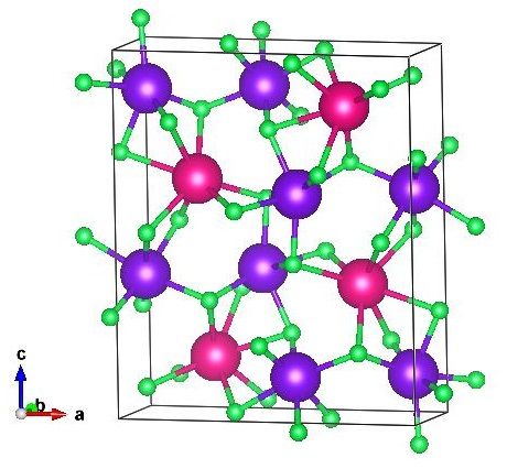
Eu3O4 crystallises into an orthorhombic structure (space group Pnma) similar to CaFe2O4 with the lattice parameters a Å, b Å and c Å [2, 3]. Figure 1 shows the Eu3O4 structure, where the Eu2+ and Eu3+ ions are occupying the Ca2+ and Fe3+ sites, respectively. The oxygen ions form a six- and eight-fold coordination around the Eu3+ and Eu2+ ions, respectively. The coordination is then completed with two oxygen ions lying at the corner of the crystal [2, 4]. Therefore, Eu3O4 has two Eu3+ and one Eu2+ ions per unit formula [4].
The compound Eu3O4 has an antiferromagnetic arrangement below 5 K. Its bulk and powder forms show a metamagnetic behaviour below the Néel temperature (TN), at a critical field of 2.4 kOe. Therefore, Eu3O4 is considered a potential material for magnetic refrigeration applications [3, 5, 4]. Although Eu3O4 is a mixed-valence compound, its magnetic ordering is mainly determined by the Eu2+ ions at low-temperature due to the high magnetic moment of Eu2+ (total angular momentum, J) in comparison to the Eu3+ ions (J) [5, 4, 3]. It has been proposed that the nearest neighbouring Eu2+ ions are strongly coupled by ferromagnetic interactions at low temperature, whereas the distant ions are coupled by weaker antiferromagnetic coupling, resulting in the overall antiferromagnetic state of Eu3O4 [5].
Graphene is a promising material for spintronics applications due to its desirable properties such as its long spin-diffusion length and high electron mobility. So far, no study on the graphene/Eu3O4 system has been reported. This may well be due to the difficulty of growing Eu3O4, which is the unstable high-temperature phase of Eu-oxides. Therefore, this study presents one of the first fundamental steps towards understanding the exchange coupling between a Eu3O4 and graphene.
In this study, 20 nm Eu3O4 thick films were grown on a Si/SiO2 substrate and graphene sheet supported on Si/SiO2 by molecular beam epitaxy (MBE) and capped with 5 nm of Au. Eu was deposited at high temperatures (300 - 600 ∘C) in an oxygen flux. The growth parameters such as the oxygen partial pressure, temperature and deposition rate were optimised to achieve a crystalline Eu3O4(001) phase. The structural characterisation of the films was studied by X-ray diffraction (XRD) and reflection (XRR), where a superconducting quantum interference device magnetometer (SQUID) was used to study their magnetic properties. The results show a successful growth of crystalline, highly-textured Eu3O4 (001) films with a Curie temperature (TC) of K, which is in agreement with the value reported in Ref. [3]. Depth-profile X-ray photon electron spectroscopy (XPS) scans were performed to prove the mixed-valence of Eu cations in Eu3O4. Furthermore, Raman spectroscopy measurements on the Si/SiO2/graphene/Eu3O4 sample showed that although the growth of Eu3O4 film induced defects in the graphene sheet, the graphene retains its hexagonal lattice structure.
II Sample Preparation
20 nm Eu3O4(001) films were deposited on cleaned Si/SiO2 and commercially purchased Si/SiO2/graphene substrates by MBE with a base pressure of 4 10-10 mbar. The substrates were heated to 400∘C, while the Eu was evaporated at a rate of 1.2 nm/min. Oxygen was then introduced into the growth chamber, resulting in a partial pressure of 1.1 10-8 mbar to deposit Eu3O4(001) at a rate of 1.11 nm/min. A 5 nm film of Au was grown subsequently on the Eu3O4(001) films to prevent them from oxidising to the most stable oxide phase of Eu (Eu2O3). The Au films were deposited at 45∘C, with a rate of 0.057 nm/min at a pressure of 1.9 10-10 mbar.
A quartz crystal microbalance was used during the deposition to monitor the growth rate and thus the thicknesses of the layers. Room temperature (RT) XRD scans were used to study the crystallinity of the grown films. The XRR measurements were then performed to confirm the results of the microbalance readings and deduce the density and roughness between the layers. These acquisitions were carried out using a Bruker D8 Discover HRXRD with a Cu K monochromatic beam with a voltage of 40 kV and a current of 40 mA. The magnetic properties of the Eu3O4 films were studied using a Quantum Design SQUID.
Depth-profile XPS scans using Al K X-ray source (1486.68 eV, beam width of 500 m) were performed on the Si/SiO2/Eu3O4/Au sample. This was done to study the homogeneity of the Eu3O4 film, determine the atomic ratio of Eu2+ and Eu3+ and confirm the mixed-valence character of the grown film. Furthermore, the effect of depositing Eu3O4 film on the graphene sheet was investigated by Raman spectroscopy measurements using a Renishaw InVia spectrometer (100 objective, 10% laser power, spot size of m, 0.5 s exposure time, a wavelength of 532 nm). However, the Au capping layer was selectively etched in KI/I2 solution before the measurements to eliminate the Au interference with the Raman measurements. The Si/SiO2/graphene/Eu3O4/Au sample was cleaved into mm square and placed in the etchant solution for 5 minutes at RT, rinsed with DI water twice, then with IPA and dried with dry N2. Raman scans were then taken at every m in a grid pattern over an area of m m for the region coated with Eu3O4, and every m over an area of m m for the bare graphene surface.
III Results and Discussion
III.1 X-ray Diffraction (XRD)
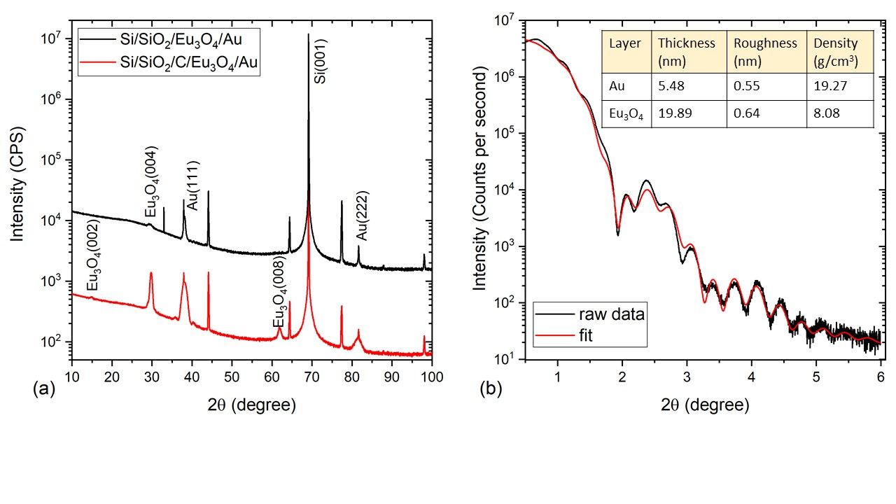
The RT XRD scans (from 20∘ - 100∘) of the Eu3O4(001) films grown on the Si/SiO2 substrate and on graphene are shown in Figure 2 (a). The XRD scans show highly textured Eu3O4(002) films with no sign of other oxide-phase of Eu or unreacted Eu within the detection limit of the set-up. Additional Eu3O4(004) and (008) peaks are observed in the scan of the Si/SiO2/graphene/Eu3O4/Au sample, indicating that the underlying graphene layer improves the crystallinity of the Eu3O4 film. This is also proven by the smaller full-width at half-maximum (FWHM) of the Eu3O4 peaks of the Si/SiO2/graphene/Eu3O4/Au sample compared to the Si/SiO2/Eu3O4/Au. Figure 2 (b) shows the XRR scan and the corresponding fit for the Si/SiO2/Eu3O4/Au sample, whereas the deduced values for the thickness, density and roughness of the layers are listed in the inset table.
III.2 SQUID
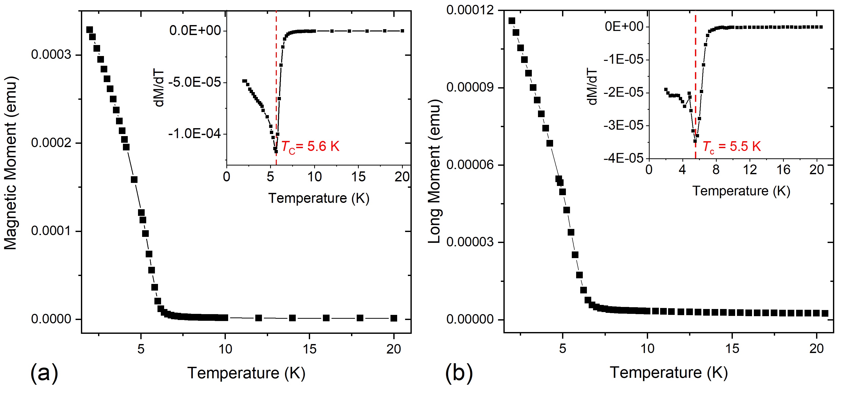
Figure 3 shows the field-cooled (FC) and zero field-cooled (ZFC) measurements of the Si/SiO2/Eu3O4(001)/Au and Si/SiO2/graphene/Eu3O4(001)/Au samples, respectively. Both show a TC of K as can be deduced from the dM/dT vs T (insets), which agrees with values reported in the literature [5, 4, 3]. Therefore, care has to be given to check for impurities of Eu3O4 phase in EuO1-x thin films which sometimes show a pronounce bump at T K [6, 7].
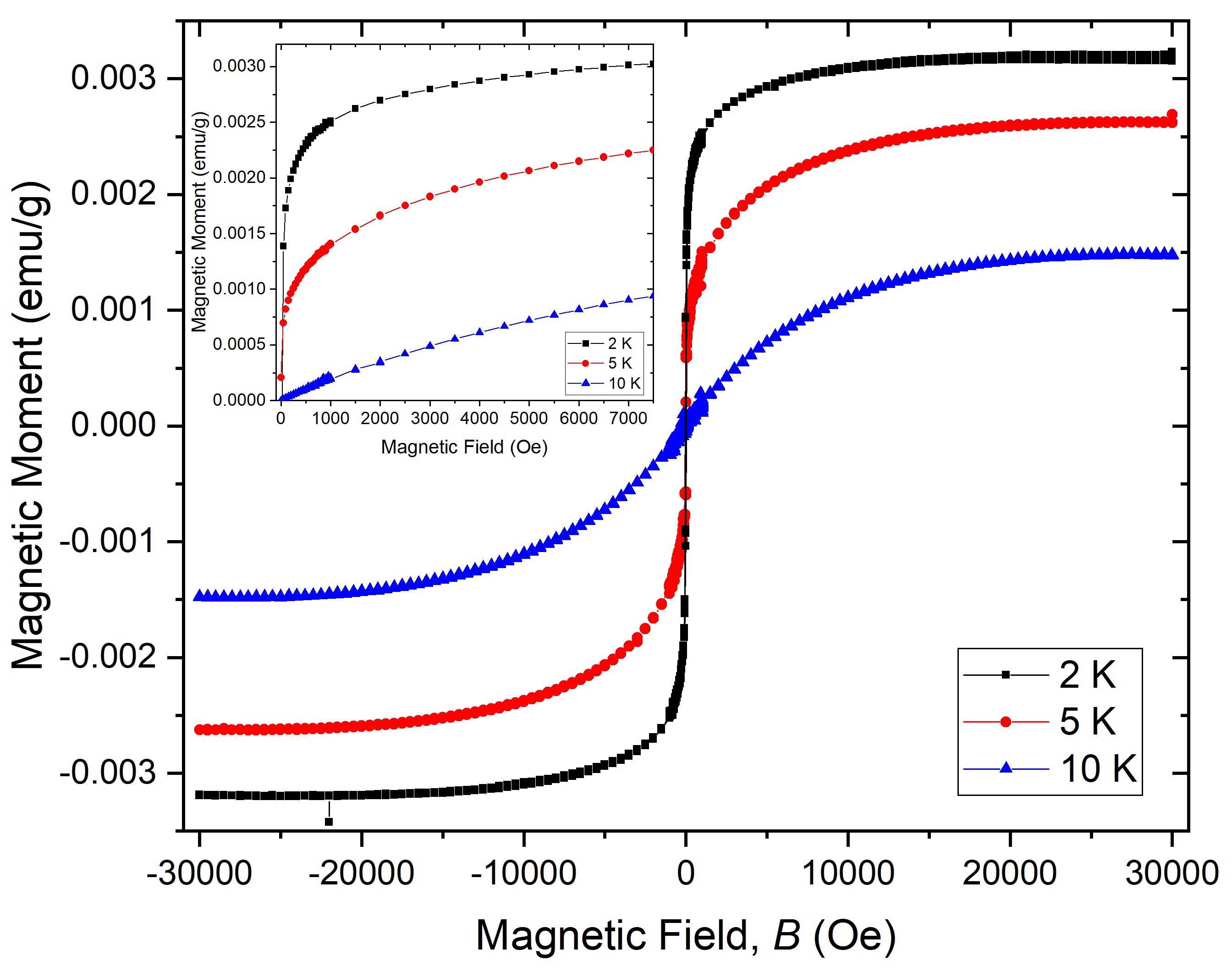
The ZFC isothermal magnetisation measurements as a function of the applied magnetic field for the Si/SiO2/graphene/Eu3O4/Au sample at 2 K, 5K and 10 K are shown in Figure 4. The hysteresis curves show that the grown Eu3O4 films exhibit ferromagnetic behaviour with a coercive field of 22 Oe. The inset highlights the virgin magnetisation curves at these temperatures. Although the XRD scans (Figure 2 (a)) and the M vs T measurements (Figure 3) prove the growth of Eu3O4(001) thin films, surprisingly, the virgin MH curves show no metamagnetic transition even with an applied in-plane magnetic field of 3 kOe as reported for crystal and powder Eu3O4 [4, 3]. This could be attributed to the strain from the substrate which could be resolved by growing a thicker film.
III.3 XPS
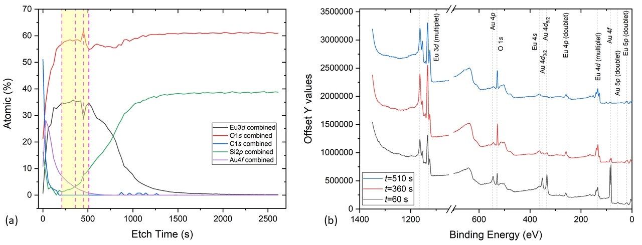
The existence of mixed-valence Eu cations was investigated by performing depth-profile XPS scans while measuring the Eu 3d and 4d spectra simultaneously after Ar+ plasma etching. Figure 5 (a) shows the XPS etch profile of the sample, whereas the XPS survey collected at t210 s, 360 s, 450 s and 510 s, highlighting the different detected elements are shown in Figure 5 (b). The 4d XPS spectra have a complicated structure (not shown) due to the strong unfilled 4fd hole interaction, whereas the 3d states have a weaker multiplet splitting and broader photoexcitation cross-section. Therefore, the latter is usually used to analyse the Eu XPS spectra and obtain a better estimation of the Eu initial valence [8, 9, 10, 11].
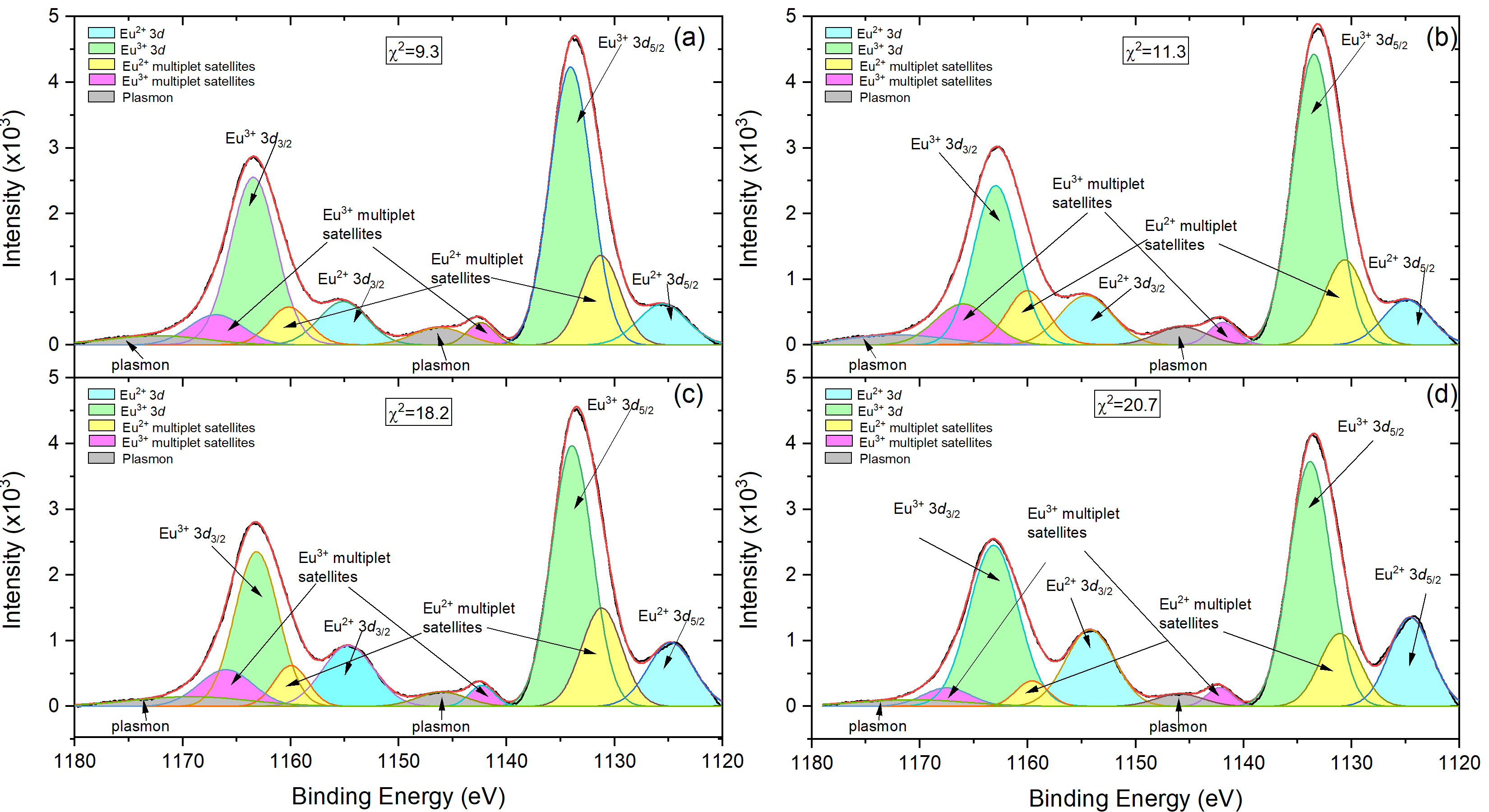
Figure 6 (a) - (d) shows the Eu 3d XPS spectra after subtracting an optimised Shirley background, measured at t210 s, 360 s, 450 s and 510 s. The peaks were deconvoluted using Gaussian-Lorentzian fitting, while the value indicates the quality of the fit. Although the Eu3O4 layer was etched fully, only these scans were considered for the analysis of the Eu cation valency (the yellow shaded area of Figure 5 (a)) to minimise the effect of interdiffusion at the SiO2/Eu3O4 and Eu3O4/Au interfaces and increase the intensity of the Eu 3d and 4d peaks.
| Spectrum | Eu2+ (eV) | |||||
| 3d5/2 | FWHM | 3d5/2 Satellites | 3d3/2 | FWHM | 3d3/2 Satellites | |
| t s | 1125.54 | 5.39 | 1131.26 | 1155.14 | 5.29 | 1160.16 |
| t s | 1124.88 | 5.17 | 1130.64 | 1154.75 | 5.76 | 1160.04 |
| t s | 1124.78 | 5.01 | 1131.19 | 1154.65 | 5.64 | 1159.96 |
| t s | 1124.56 | 4.58 | 1131.07 | 1154.21 | 5.36 | 1159.58 |
| Eu3+(eV) | ||||||
| 3d5/2 | FWHM | 3d5/2 Satellites | 3d3/2 | FWHM | 3d5/2 Satellites | |
| t s | 1134.07 | 4.56 | 1142.39 | 1163.46 | 5.03 | 1166.92 |
| t s | 1133.49 | 4.69 | 1141.90 | 1162.96 | 4.85 | 1166.00 |
| t s | 1133.93 | 4.46 | 1142.29 | 1163.15 | 4.80 | 1166.00 |
| t s | 1133.83 | 4.56 | 1142.23 | 1163.15 | 5.38 | 1167.48 |
| Atomic ratio 3d5/2 | Atomic ratio 3d3/2 | |||||
| Eu2+ | Eu3+ | Eu2+ | Eu3+ | |||
| t s | 49.81 | 50.19 | 21.39 | 78.61 | 9.30 | |
| t s | 14.63 | 85.37 | 26.84 | 73.16 | 11.30 | |
| t s | 21.58 | 78.42 | 31.61 | 68.39 | 18.20 | |
| t s | 26.80 | 73.20 | 31.96 | 68.04 | 20.70 | |
| Average | 28.20 | 71.80 | 27.95 | 72.05 | ||
All spectra in Figure 6 show the spin-orbit coupling (SOC) components, 3d5/2 and 3d3/2, for Eu2+ and Eu3+ separated by eV, which agrees with previously reported values [10, 8, 12]. They also show additional peaks at slightly higher binding energy (BE) to the SOC peaks for the Eu2+ and Eu3+. These shake-up satellite peaks arise as a result of the multiplet structures of the 4fd hole in the final state [11]. Furthermore, the fast 3d photoelectrons create plasmon excitation structures observed as broad peaks at BE eV and eV [8]. The XPS spectra shown in Figure 6 prove the mixed-valency of Eu cations as they agree well with previous work reported for Eu2+ and Eu3+ [8, 10, 13, 14, 15]. Moreover, the average atomic ratio of the Eu2+ to Eu3+ in the 3d5/2 and 3d3/2 is consistent with the values reported in Eu-doped ZnO [16] and Eu-doped GaN nanowires [17]. Table 1 summarises the positions of the Eu2+ and Eu3+ 3d peaks, their FWHM, their corresponding multiplet satellites, the ratio of Eu2+/Eu3+ and the fits values of the four spectra.
III.4 Raman Spectroscopy
Raman spectroscopy is a versatile and non-destructive technique widely used to study the structural and electronic properties of graphene [18, 19]. A good-quality monolayer of graphene has two main characteristic Raman peaks; the G and 2D peaks at cm-1 and cm-1, respectively. It can also possesses other disorder-induced peaks such as the D peak at cm-1 [20, 21, 22]. Therefore, the presence or absence of these peaks and the ratio of the intensity of the D peak to the intensity of the G peak (ID/IG), which represents the defect density in the graphene structure, were mostly used to assess the quality of our graphene underlayer [23].
Figure 7 (a) and (b) show the microscopic optical images of the sample highlighting three different regions of the Si/SiO2/graphene/Eu3O4/Au sample taken before etching the Au capping layer. The zoom-in image collected with a objective lens (Figure 7 (b)) shows that the graphene layer consists of a mixture of mono- and multilayer graphene domains rather than a continuous homogeneous monolayer, which could be either a result of the growth of the Eu3O4 film or the pristine quality of the commercial graphene. Therefore, one would expect the presence of defect-induced peaks in the Raman scans [23].
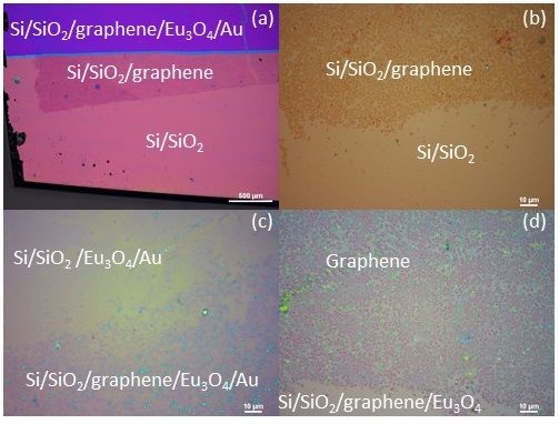
Figure 7 (c) and (d) show the microscopic optical images of the graphene edge under the Eu3O4 film before and after removing the Au layer, respectively. No significant change in the contrast is observed between the two images suggesting that the etching process did not remove or affect the graphene underlayer.
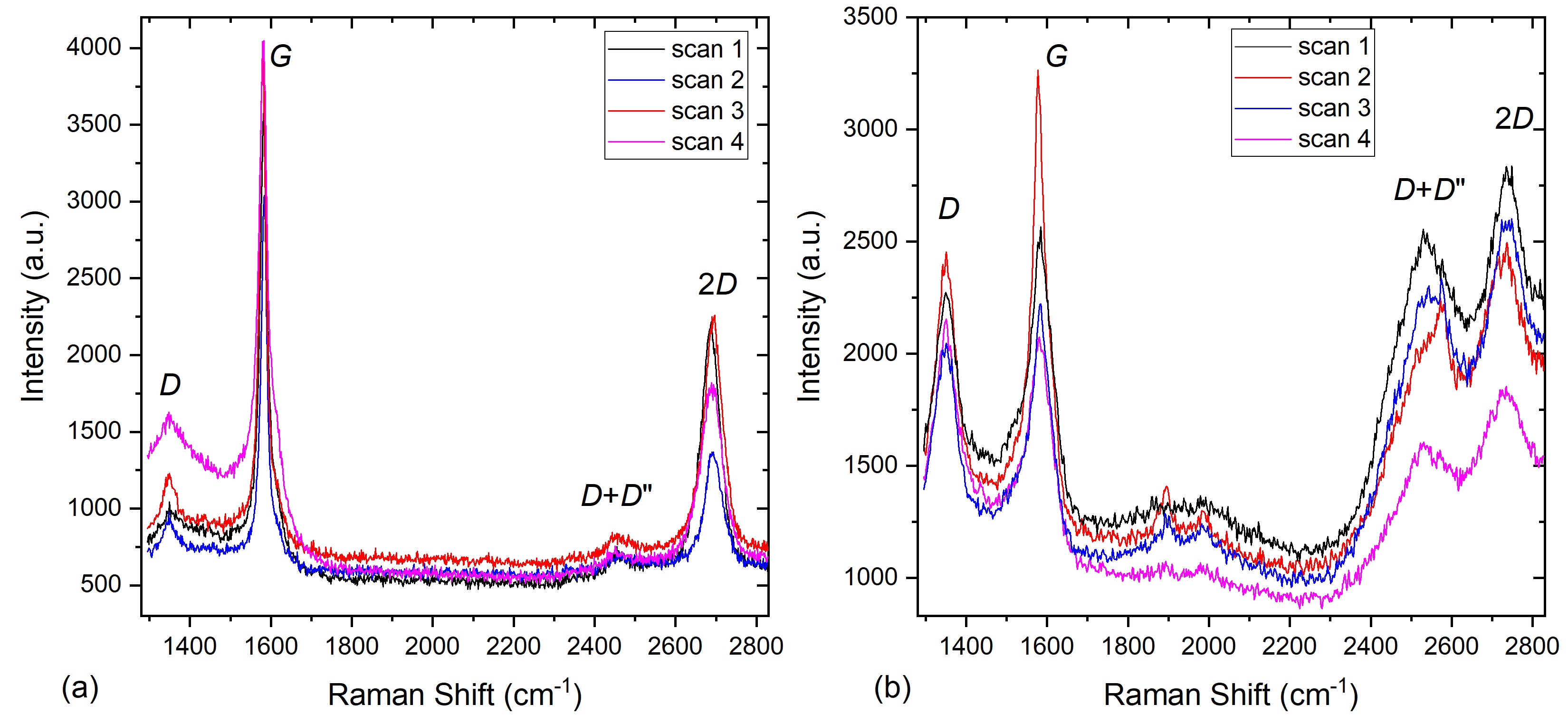
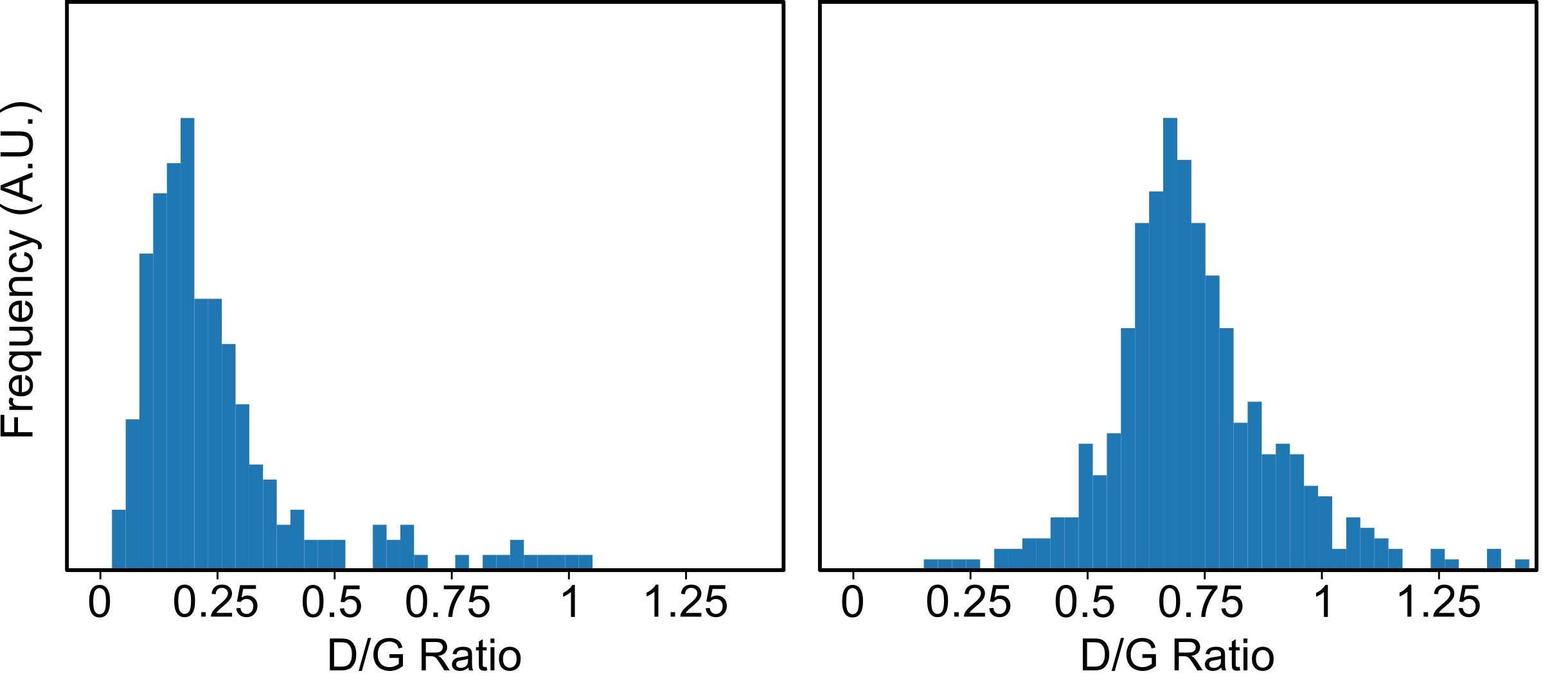
Four random Raman scans taking on two different areas of the sample’s surface; bare graphene and the graphene/Eu3O4 region after removing the Au layer are shown in Figure 8 (a) and (b), respectively. The emergence of the additional defect-induced peaks in the spectra of the graphene/Eu3O4 area and the increase in their intensities (Figure 8 (b)) compared to the scans of the bare graphene (Figure 8 (a)) indicates that the growth of Eu3O4 film increased the defect density in the graphene structure. This is also seen by the shift in the ID/IG ratio of the graphene under the Eu3O4 film towards the higher values, compared to the bare graphene sheet (Figure 9). This is because ID/IG is known to be small for low-defect-density graphene [22, 24]. However, since the underlayer graphene is visible with the optical microscope (Figure 7) and that the Raman characteristic features of graphene are maintained after the growth of the Eu3O4 film (Figure 8), one would expect the graphene underlayer to retain its properties.
IV Conclusion
In summary, we discussed the experimental work carried out to study the growth of Eu3O4 thin film by MBE on Si/SiO2 and on a graphene sheet. The structural and magnetic characterisations show successful deposition of crystalline, highly-textured Eu3O4(001) films with a TC of K. However, the films show no metamagnetic behaviour which could be attributed to the strain from the substrate. Furthermore, a qualitative analysis of the XPS scans confirms the mixed-valency of the Eu cation.
Raman measurements show that the graphene layer retained its hexagonal lattice structure under the Eu3O4 film. Therefore, this study represents the first successful step towards integrating a Eu3O4 thin film in two widely used electronic substrates for future spintronics applications.
Acknowledgements.
Authors would like to acknowledge David Love and Pedro M S Monteiro for their support.References
- Varma [1976] C. M. Varma, Mixed-valence compounds, Reviews of Modern Physics 48, 219 (1976).
- Rau [1966] R. C. Rau, The crystal structure of Eu3O4, Acta Crystallographica 20, 716 (1966).
- Ahn et al. [2009] K. Ahn, V. K. Pecharsky, and K. A. Gschneidner, The magnetothermal behavior of mixed-valence Eu3 O4, Journal of Applied Physics 106, 043918 (2009).
- Holmes and Schieber [1966] L. Holmes and M. Schieber, Magnetic Ordering in Eu3O4 and EuGd2O4, Journal of Applied Physics 37, 968 (1966).
- Holmes and Schieber [1968] L. Holmes and M. Schieber, Metamagnetism in Eu3O4, Physical Review 167, 449 (1968).
- Liu and Tang [2012] P. Liu and J. Tang, Antiferromagnetic coupling in EuO1-x, Physical Review B 85, 224417 (2012).
- Liu and Tang [2013] P. Liu and J. Tang, A magnetic polaron model for the enhanced Curie temperature of EuO 1- x, Journal of Physics: Condensed Matter 25, 125802 (2013).
- Caspers et al. [2011] C. Caspers, M. Müller, A. X. Gray, A. M. Kaiser, A. Gloskovskii, C. S. Fadley, W. Drube, and C. M. Schneider, Chemical stability of the magnetic oxide EuO directly on silicon observed by hard x-ray photoemission spectroscopy, Physical Review B - Condensed Matter and Materials Physics 84, 1 (2011).
- Cho et al. [1996] E.-J. Cho, T. Oh, S.-J. Suzuki, and T. Kasuya, Electronic structure study of Eu intermetallic compounds by photoelectron spectroscopy, Journal of Electron Spectroscopy and Related Phenomena 77, 173 (1996).
- Mariscal et al. [2018] A. Mariscal, A. Quesada, A. T. Martín-luengo, M. A. García, A. Bonanni, J. F. Fernández, and R. Serna, Applied Surface Science Europium monoxide nanocrystalline thin films with high near-infrared transparency, Applied Surface Science 456, 980 (2018).
- Cho, En-Jin and Oh, S.-J. and Imada, S. and Suga, S. and Suzuki, T. and Kasuya [1995] T. Cho, En-Jin and Oh, S.-J. and Imada, S. and Suga, S. and Suzuki, T. and Kasuya, Origin ofthe high-binding-energy structure in the 3d core-level spectra of divalent Eu compounds, Physical Review B 51, 10146 (1995).
- Orlowski et al. [2005] B. A. Orlowski, S. Mickievicius, V. Osinniy, A. J. Nadolny, and B. Taliashvili, High-energy X-ray photoelectron spectroscopy study of MBE grown ( Eu , Gd ) Te layers, Nuclear Instruments and Methods in Physics Research B 238, 346 (2005).
- Ohno and Urata [2002] Y. Ohno and T. Urata, Photoelectron spectra and surface valence fluctuation of Eu in the misfit-layer compound {(EuS)1.15}1.5NbS2, Journal of Electron Spectroscopy and Related Phenomena 125, 171 (2002).
- Kim et al. [2019] D. Kim, J. R. Jeong, Y. Jang, J.-S. Bae, I. Chung, R. Liang, D.-K. Seo, S.-J. Kim, and J.-C. Park, Self-emitting blue and red EuOX (X = F, Cl, Br, I) materials: band structure, charge transfer energy, and emission energy, Physical Chemistry Chemical Physics 21, 1737 (2019).
- Cho and Oh [1999] E. Cho and S.-J. Oh, Surface valence transition in trivalent Eu insulating compounds observed by photoelectron spectroscopy, Physical Review B 59, 3 (1999).
- Lupan et al. [2013] O. Lupan, T. Pauporté, B. Viana, P. Aschehoug, M. Ahmadi, B. R. Cuenya, Y. Rudzevich, Y. Lin, and L. Chow, Eu-doped ZnO nanowire arrays grown by electrodeposition, Applied Surface Science 282, 782 (2013).
- Faye et al. [2019] D. N. Faye, X. Biquard, E. Nogales, M. Felizardo, M. Peres, A. Redondo-Cubero, T. Auzelle, B. Daudin, L. H. Tizei, M. Kociak, P. Ruterana, W. Möller, B. Méndez, E. Alves, and K. Lorenz, Incorporation of Europium into GaN Nanowires by Ion Implantation, Journal of Physical Chemistry C 123, 11874 (2019).
- Wang et al. [2008] Y. Y. Wang, Z. H. Ni, Z. X. Shen, H. M. Wang, and Y. H. Wu, Interference Enhancement of Raman Signal of Graphene, Applied Physics Letters 92, 10.1063/1.2838745 (2008), arXiv:0801.4595 .
- Chilres et al. [2013] I. Chilres, L. A. Jauregui, W. Park, H. Cao, and Y. P. Chen, Raman Spectroscopy of Viruses and Viral Proteins, in New Developments in Photon and Materials Research, edited by J. I. Jang (Nova Science Publishers, Incorporated, 2013) Chap. 19, pp. 553–595.
- Allard and Wirtz [2010] A. Allard and L. Wirtz, Graphene on Metallic Substrates: Suppression of the Kohn Anomalies in the Phonon Dispersion, Nano Letters 10, 4335 (2010).
- Malard et al. [2009] L. M. Malard, M. A. Pimenta, G. Dresselhaus, and M. S. Dresselhaus, Raman Spectroscopy in Graphene, Physics Reports 473, 51 (2009).
- Shlimak et al. [2015] I. Shlimak, A. Haran, E. Zion, T. Havdala, Y. Kaganovskii, A. V. Butenko, L. Wolfson, V. Richter, D. Naveh, A. Sharoni, E. Kogan, and M. Kaveh, Raman Scattering and Electrical Resistance of Highly Disordered Graphene, Physical Review B 91, 045414 (2015).
- Aboljadayel et al. [2021] R. O. M. Aboljadayel, D. M. Love, C. A. F. Vaz, R. S. Weatherup, P. Braeuninger-Weimer, M. B. Martin, A. Cabrero-Vilatela, A. Ionescu, C. J. Kinane, T. R. Charlton, J. Llandro, P. M. S. Monteiro, C. H. W. Barnes, S. Hofmann, and S. Langridge, Determining the Proximity Effect Induced Magnetic Moment in Graphene by Polarised Neutron Reflectivity and X-ray Magnetic Circular Dichroism, , 1 (2021), arXiv:2101.09946 .
- Cabrero-Vilatela et al. [2016] A. Cabrero-Vilatela, R. S. Weatherup, P. Braeuninger-Weimer, S. Caneva, and S. Hofmann, Towards a General Growth Model for Graphene CVD on Transition Metal Catalysts, Nanoscale 8, 2149 (2016).