Ni80Fe20 Nanotubes with Optimized Spintronic Functionalities Prepared by Atomic Layer Deposition
Maria Carmen Giordano,a Simon Escobar Steinvall,b Sho Watanabe,a Anna Fontcuberta i Morral,b,c and Dirk Grundler∗a,d
Abstract: Permalloy \ceNi80Fe20 is one of the key magnetic materials in the field of magnonics. Its potential would be further unveiled if it could be deposited in three dimensional (3D) architectures of sizes down to the nanometer. Atomic Layer Deposition, ALD, is the technique of choice for covering arbitrary shapes with homogeneous thin films. Early successes with ferromagnetic materials include nickel and cobalt. Still, challenges in depositing ferromagnetic alloys reside in the synthesis via decomposing the consituent elements at the same temperature and homogeneously. We report plasma-enhanced ALD to prepare permalloy \ceNi80Fe20 thin films and nanotubes using nickelocene and iron(III) tert-butoxide as metal precursors, water as the oxidant agent and an in-cycle plasma enhanced reduction step with hydrogen. We have optimized the ALD cycle in terms of Ni:Fe atomic ratio and functional properties. We obtained a Gilbert damping of 0.013, a resistivity of 28 cm and an anisotropic magnetoresistance effect of 5.6 in the planar thin film geometry. We demonstrate that the process also works for covering GaAs nanowires, resulting in permalloy nanotubes with high aspect ratios and diameters of about 150 nm. Individual nanotubes were investigated in terms of crystal phase, composition and spin-dynamic response by microfocused Brillouin Light Scattering. Our results enable NiFe-based 3D spintronics and magnonic devices in curved and complex topology operated in the GHz frequency regime.
1 Introduction
Magnetic thin films play an extremely important role in technologies such as data storage media1, GMR sensors 2, spin valves3 and magnetic MEMS 4, 5. Among various magnetic materials, the NiFe alloy with stoichiometry \ceNi80Fe20, often referred as permalloy, is technologically relevant for the high permeability, low coercivity, near zero magnetostriction and significant anisotropic magnetoresistance (AMR).
Permalloy plays a crucial role also in fundamental and applied research, as it is one of the standard materials chosen for the study of novel structures in nanomagnetism and magnonics6, 7. The latter is a modern branch of magnetism focused on the study of the spin waves, the collective excitations of magnetically ordered materials. Low energy consumption of spin waves and the potential compatibility with next-generation circuits beyond CMOS electronics make them a potential tool for non-charge based signal processing, communication and computation 7, 8, 9, 10. In magnonics, the choice of magnetic materials would fall on those with low damping for spin waves, a property quantified by the phenomenological dimensionless Gilbert damping parameter . Standard materials would be insulating magnets as yttrium iron garnet (YIG) and polycristaline metallic alloys as NiFe and CoFeB. While YIG offers the lowest spin wave damping, the choice of polycristaline metallic alloys as NiFe and CoFeB meets better the needs for the industrial scalability of miniaturized and integrated systems11.
So far, \ceNi80Fe20 films have been mostly obtained by physical vapor deposition (PVD) methods, like sputtering 12, 13, electron beam evaporation and molecular beam epitaxy14. Other routes are electrodeposition15, 16, 17, 18, spray coating and micromolding 19. The PVD techniques are well suited for the production of planar nanostructures20, 21. However, they are limited by shadowing effects, which make them disadvantageous for the coating of three-dimensional (3D) nanostructures with high aspect ratios. Correspondingly, tetrapods for multi-branched 3D spintronics were prepared from polycrystalline cobalt by means of electrodeposition 22. To further optimise the deposition of 3D permalloy coatings, it is a necessity to increase the step edge coverage. This enhances the deposition uniformity irrespective of the morphology of the deposited surface, and in turn opens up the study of new physical phenomena envisioned in 3D nanomagnetic systems 23, 11, 24, 25, 26, 27, 6, 28, 29.
Atomic layer deposition (ALD) is a chemical deposition technique offering the ideal conformality on 3D nanostructured surfaces. Here, the thin film formation is based on the repeated exposure of a substrate to separate precursors 30, 31. These precursors react with the surface of a material one at a time in a sequential, self-limiting manner ensuring a good control of thickness, excellent step coverage and conformality on substrates with different geometries and aspect ratios. The deposition of high- gate oxides, such as \ceAl2O3, has been one of the most widely examined areas of ALD and already advances microelectronics applications like metal-oxide semiconductor field effect transistors (MOSFET) and dynamic random access memories (DRAM)32. The processes for depositing metal layers using this technique, including ferromagnetic metals, still present technical challenges and are the subject of extensive research 33, 34, 35, 36, 37. The main challenges are the limited number of suitable precursors, the difficulty in reducing metal cations and the tendency of metals to agglomerate into islands 37, 33. We emphasize the difficulty, specific to a bi-metallic alloy, to identify a pair of precursors, one for each metal, which have a similar reactivity with the substrate surface, with a suitable co-reactant and in the same thermal range. Many works concern the use of ALD to obtain 3D nickel nanostructures such as nanotubes 38, 39, 40, 41, 42, 43. The research on NiFe metallic alloys deposited by ALD is still in its infancy. Ferrimagnetic oxides NixFe have been successfully prepared by exploiting the ALD process of the two binary oxides NiO and FeO 44. In the work of Espejo 45 a study was presented where a combination of supercyclic ALD with thermal reduction is used to achieve metallic alloy NiFe thin films. The process explored was based on nickelocene and ferrocene as Ni and Fe precursors, ozone as co-reactant to get an intermediate NiFe oxide and a further annealing in hydrogen. A linear dependency between the Ni : Fe precursors pulse ratio and the final stoichiometry was identified, leading to the achievement of a NiFe stoichiometry (\ceNi83Fe17) very close to that of permalloy. The study showed how the initial amount of oxygen in the NiFe - oxide thin films obtained induces a significant dewetting phenomenon during the thermal reduction in hydrogen, compromising the morphology in the final metallic form.
In this work we present a different approach where the nickel (iron) sequence exploits nickelocene (iron(III) tert-butoxide) as metal precursors, water as the oxidant agent and an in-cycle plasma enhanced reduction step with hydrogen. Ni-rich NiFe thin films with different Ni:Fe atomic ratios were achieved by alternating times the sequence for the deposition of nickel 46, 47 with a single sequence for the deposition of oxidized iron 48, 49, 50 and a post-deposition annealing treatment in hydrogen.
The planar thin films so prepared were characterized in terms of a series of electric and magnetic properties considered significant for industrial applications and research. We quantitatively compare them with thin films that we prepared by the electron-beam evaporation using a commercial \ceNi80Fe20 target material.
The sequence with optimized Ni:Fe pulse ratio , combined with the post-processing annealing treatment, allowed us to prepare thin films with the expected \ceNi3Fe FCC phase () 51, stoichiometry extremely close to target permalloy (Ni80.4Fe19.6) and physical properties unprecedently measured in permalloy thin films prepared by ALD. We measured a coercive field of 3.6 mT, a Gilbert damping of 0.013 and a resistivity of 28 cm. The process presented could contain the dewetting phenomenon on silicon substrates. As a proof of concept for the use of this technique to obtain nanostructured 3D coatings, we show the fabrication of NiFe nanotubes (NTs) using GaAs nanowires (NWs) with high aspect ratio and diameters lower than 100 nm as nanotemplates. We provide a chemical and structural characterization of the NiFe nanotubes, confirmed to have a permalloy shell. Lastly, the low damping of the ferromagnetic shell allowed to measure several spin waves resonant modes in individual NTs investigated by micro-focused Brillouin Light Scattering (-BLS). Our results show the remarkable potential of the ALD technique to venture the third dimension in nanomagnetism, magnonics and spintronics applications based on thin-film permalloy prepared by conformal coating technique.
2 Results and discussion
2.1 Morphology of Nickel-Iron Thin Films and Nanotubes
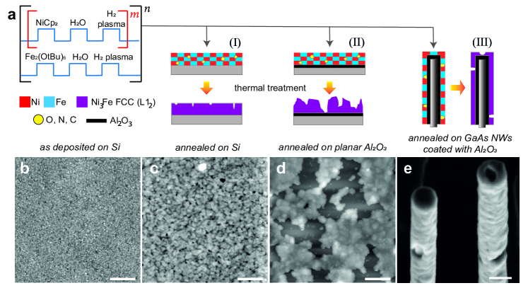
In Figure 1a we show schematically the process followed to prepare Ni100-xFex thin films by plasma enhanced atomic layer deposition (PEALD) on different substrates. The PEALD cycle combines a sequence for the deposition of nickel47, 46 and a sequence for the deposition of \ceFe2O348, 49, 50, to which we have added a plasma hydrogen step. The Ni:Fe atomic ratio is controlled by the number of the Ni sequence repetition between each Fe step.
The NiFe process was tested on relevant substrates like planar Si wafers, both uncoated and coated with few nm of alumina \ceAl2O3, and GaAs NWs encapsulated in a capping layer of \ceAl2O3. The as-deposited films were annealed aiming at the \ceNi3Fe FCC phase. We show the AFM analysis performed on the sample prepared with in its as-deposited (Figure 1b) and annealed state (Figure 1c) on a bare Si substrate. In Figure 1d we report the AFM analysis on the annealed thin film obtained with the same process, exploiting , on a Si substrate coated with 5 nm of alumina. Lastly, the SEM micrograph in Figure 1e depicts the morphology of the thin films deposited on GaAs/\ceAl2O3 nanowires, once the annealing treatment is performed. Depending on the type of substrate, the thermal treatment was found to have different effects on the final morphology of the thin films. In general, on a bare Si substrate, we observe that the annealing process is accompanied by a thin film thickness shrinkage of about 15 , the formation of nanopores and a higher surface roughness with respect to the as-deposited thin film. For the reported sample the rms roughness increased from 1.2 nm to 2.1 nm in thin films with a thickness of 27 nm and 23 nm, respectively, in the as-deposited (Figure 1b) and annealed form (Figure 1b). For the Si substrate coated with alumina we observe that the thermal treatment is accompanied by a dewetting of the thin film. Here, the thin film arranges in agglomerates to reduce the film-substrate interface area and minimize the system energy. In Fig. 1e, we observe the formation of random localized small holes in the 3D shells achieved by coating GaAs/\ceAl2O3 NWs. Despite the unfavorable adhesion of Ni100-xFex on the alumina layer, the encapsulation of GaAs nanowires by few nm of this material was necessary to prevent the As evaporation during the annealing and to use them as a template for Ni100-xFex nanotubes.
The same experiments were done with Ni : Fe pulse ratio 4 . The thermal treatment was performed for all the compositions. All the samples were amorphous and contained remaining oxygen, nitrogen and carbon in their as-deposited state (Figure S1). The types of morphology described are common to the samples obtained with the synthesis parameter m = 4, 5 and 6. For the sample prepared with m = 7, more nanoholes are observed (Figure S2). For this sample, we speculate that phase segregation might have further increased its roughness and the number of holes during the annealing treatment and subsequent cooling, as its composition might be close to the \ceNi90Fe10 phase segregation line in the Ni-Fe phase diagram 51.
2.2 Growth rates
The choice of the homoleptic dinuclear iron(III) tert-butoxide complex (\ceFe2(OtBu)6) as iron precursor is motivated by its capability to react with water in a self-limiting manner. Furthermore, it reacts at temperatures (C 48, 49, 50) compatible with the one for the deposition of nickel using nickelocene (\ceNiCp2), water and plasma hydrogen as reactants (C in our system 46). The growth rate of the processes exploiting and 7 was estimated to be (0.15, 0.17, 0.18 and 0.20) Å/ cycle, respectively. The recorded values were lower than those that would be obtained for the Ni and \ceFe2O3 processes individually. We hypothesize that the deposition of Ni in the presence of \ceFe2O3 is slower than in the presence of Ni alone and that a partial reduction of \ceFe2O3 in the presence of Ni and plasma hydrogen during the deposition sequence occurs. The in-depth study of these co-deposition mechanisms is not the subject of this work.
2.3 Stoichiometry and Crystallographic Analyisis of Ni100-xFex Thin Films
Figure 2 shows the X-ray diffractograms (XRD) of the annealed planar thin films prepared by PEALD with and , compared with the diffractogram of an electron-beam evaporated thin film of commercial permalloy \ceNi80Fe20, displayed at the top of the graph.
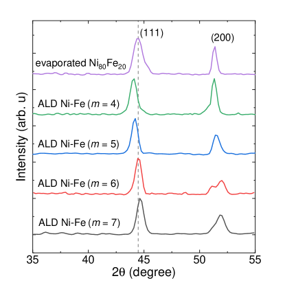
The XRD results show mainly two peaks compatible with the (111) and (200) reflections of the \ceNi3Fe FCC phase (ICSD code: 632930). The gray dotted line marks the position of the (111) reflection of the permalloy thin film evaporated from commercial target material. The (111) peak linewidth and position are reported in Table 1 for each sample. The small linewidth of the ALD thin films, compared to the reference permalloy sample, reflects a larger average crystallite size. We attribute this observation to the higher temperatures experienced both during the deposition and the annealing process by the samples prepared by ALD. The shift towards a lower angle of the (111) peak, going from the sample prepared with to the one prepared with , reflects the lattice expansion caused by the incorporation of a higher atomic percentage of Fe. The EDS analysis on the samples (Table 1) confirms this hypothesis.
| Ni:Fe pulse ratio | Ni (at) | Fe (at) | Phase | (111) peak position | Lattice parameter | |
|---|---|---|---|---|---|---|
| () | () | (Å) | ||||
| 4 | 76 5 | 24 5 | FCC () | 44.063 | 0.634 | 3.557 |
| 5 | 78 5 | 22 5 | FCC () | 44.167 | 0.543 | 3.549 |
| 6 | 81 5 | 19 5 | FCC () | 44.493 | 0.544 | 3.524 |
| 7 | 83 5 | 17 5 | FCC () | 44.666 | 0.615 | 3.511 |
| Evaporated \ceNi80Fe20 | 80 5 | 20 5 | FCC () | 44.666 | 0.802 | 3.525 |
Remarkably, the Fe incorporation in the lattice is accompanied by the appearance of stress in the film, which involves strains of the (200) plane. This is particularly visible in the diffractogram of the sample prepared with where we can distinguish two components of the (200) reflection, possibly indicating that the stress relaxation was achieved by the formation of two domains with different (200) spacing. The lattice parameter of the samples was determined based on the (111) position (Table 1). The lattice parameter is found to scale linearly with the iron content in this composition range. The lattice constant of the permalloy thin film reference, as well as the Ni:Fe atomic ratio measured by the SEM-EDS analysis, match closely the parameters obtained for the ALD sequence with Ni:Fe pulse ratio . For this pulse ratio in particular we verified the stoichiometry and the phase of the Ni100-xFex thin films obtained in the shape of nanotubes, with higher resolution techniques.
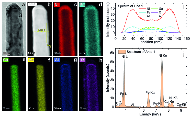
In Figure 3 (and Figure S3) we report on the elemental analysis by STEM-EDX of NiFe nanotubes deposited with the Ni:Fe precursor pulse ratio . In particular, Figure 3a and Figure 3b show a bright field TEM image and the HADDAF image of the nanotube, respectively. In Figure 3c-h the element distribution of Ni, Fe, Ga, As, Al and O are reported. In Figure 3i and Figure 3j we report the elements distribution along the Line 1 and the EDX spectra of the Area 1 depicted in Figure 3b , respectively. The NT images present a very smooth Ni-Fe shell, with no visible holes on a length of 350 nm. The core remained pristine despite the high-temperature annealing conditions. The elemental maps show a homogeneous intermixing of Ni and Fe in the outer shell (Figure 3c,d), a GaAs nanowire core (Figure 3e,f) and an intermediate alumina capping layer (Figure 3g,h). Apart from the expected presence of oxygen in the \ceAl2O3 layer at the interface between the GaAs core and Ni-Fe shell, the oxygen is almost absent in the outer shell, indicating that the thermal treatment in hydrogen successfully reduced the oxidized metal atom (Figure 3h). The elemental distribution along Line 1 shows at which position, in the 3D object, we measure the higher counts of each element. This analysis confirms that the elements of the three layers did not intermix with each other. The chemical analysis of Area 1 gives the following composition: 77.4 at Ni, 19.1 at Fe, 3.5 at O. The final NT material has, therefore, a Ni:Fe atomic ratio equal to 80.2 : 19.8 and a content of oxygen equal to 3.5 at. For this batch of NTs, we estimated an average stoichiometry of Ni80.4±0.3Fe19.6±0.3, based on the analysis of five elements (Figure S3, Table S1). The amount of oxygen within the shell of the NTs has been quantified as () at and is compatible with a small superficial passivation of the shell. After having verified the NTs stoichiometry, we analyzed the crystal phase of the 3D coatings by high resolution transmission electron microscopy (HR-TEM).
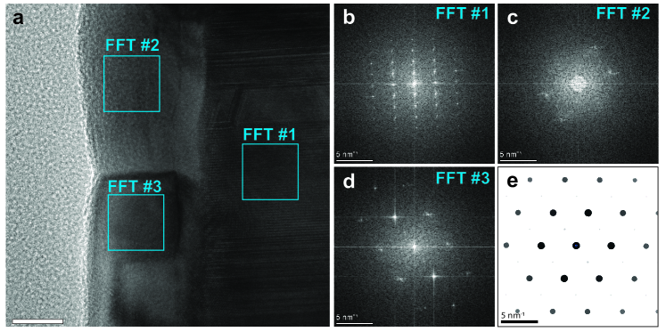
Figure 4a shows an HR-TEM image of the interface between the NiFe / \ceAl2O3 nanotube, prepared by ALD, and the GaAs nanowire core. The NiFe shell results locally compact and smooth. We took the fast Fourier transform (FFT) of the HR-TEM image in correspondance of the regions highlighted by blue squares. The extracted power spectra of the spatial frequencies are reported in Figure 4 b-d, and show the single-crystal GaAs core (Fig. 4b), and the nanocrystalline \ceNi80Fe20 shell (Fig. 4c,d). The observed pattern, and thus the orientation, varies between the \ceNi80Fe20 grains in the shell, indicative of a random crystal orientation. The symmetry of the pattern from the bottom grain (Fig. 4d) can be matched to a simulated SAED pattern of \ceNi3Fe (Fig. 4e) along a [101] zone axis. This shows that the nanotube growth occurs in a randomly oriented nanocrystalline fashion with the standard \ceNi3Fe FCC permalloy crystal structure ().
2.4 Magnetic Properties of Ni100-xFex Thin Films
The magnetic hysteresis of the as-deposited and annealed planar Ni100-xFex thin films prepared by PEALD was acquired at room temperature using a vibrating-sample magnetometer (VSM). The ALD thin films show a weak magnetization in their as-deposited state (Figure S4). Here we focus on the hysteresis of the annealed thin films prepared with Ni:Fe pulse ratios and and compare the results with the hysteresis of the reference \ceNi80Fe20 thin film. Figure 5a (Figure S5) shows the hysteresis obtained with the field applied in plane at zero (45) degrees with respect to the edge of a squared sample. In Figure 5b we report the extrapolated values of coercive field as a function of the synthesis parameter . As a reference we report, in yellow, the range of coercive field values reported for permalloy in literature 52, 53 and, marked with a dotted line, the value measured of the reference \ceNi80Fe20 thin film. The four ALD-prepared samples were ferromagnetic at room temperature and exhibited a coercive field which stayed constant with the angle of the applied field (Figure S5). A hysteresis squareness above 0.9 for samples prepared with and 6 and equal to 0.8 for the sample prepared with indicated that the magnetocrystalline anisotropy overall was small in the alloys 54. The coercive fields measured for ALD-prepared Ni100-xFex thin films ranged from 3.6 to 10 mT, with the minimum value being measured for the thin film prepared with Ni:Fe pulse ratio . The coercive field of 3.6 mT was close to the values of 0 to 3 mT expected for permalloy 52, 53 and one order of magnitude smaller than the value of 47.5 mT reported earlier for ALD-prepared Ni100-xFex thin films 45. The evaporated reference \ceNi80Fe20 thin film exhibited a coercive field of 0.36 mT. We attribute the discrepancy between the coercive fields of ALD-prepared Ni100-xFex and evaporated commercial \ceNi80Fe20 thin films to the nanoholes induced by the annealing treatment of the ALD-prepared thin films. These defects might act, in fact, as domain wall pinning centers in the ALD-grown material, affecting the magnetization reversal.
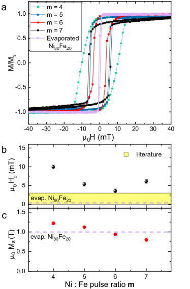
In Figure 5c, the saturation magnetization values extracted from the hysteresis are shown as a function of . The values of rang from 0.80 to 1.22 T and are found to scale linearly with the content of iron, i.e. decreases with the Ni:Fe pulse ratio . The sample prepared with exhibits a saturation magnetization of 0.94 T, which is close to the value measured for permalloy (1T).
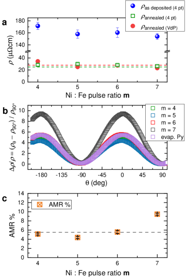
In Figure 6a we show the measured values for the resistivity both in the as-deposited and in the annealed thin films, as a function of the parameter . The resistivities measured for the annealed Ni100-xFex thin films have been obtained with a commercial 4-point probe station and a custom-built Van der Pauw configuration measurement setup. The dashed lines correspond to the resistivity values measured on a 20 nm thin film of evaporated \ceNi80Fe20. In Figure 6b, we depict the magnetoresistance measured on planar NiFe thin films when an applied in-plane magnetic field = 80 mT was rotated. The angle was defined between the current direction and H. We display the anisotropic magnetoresistance (AMR) as = . The relative AMR effect is reported in Figure 6c as a function of the synthesis parameter . We obtain resistivity values ranging from 154 to 172 cm for the as-deposited thin films. The resistivity is found to decrease with increasing , hence with the nickel content. Our resistivity values are much lower when compared with those obtained in the process that used ozone as a co-reactant 45, 43. We attribute this observation to the reduced amount of oxygen in the as-deposited material, that we achieved by the specific choice of precursors and reactants. The values of resistivity range from 23 to 34 cm in the annealed samples and do not vary significantly with . At we get = 28 cm. The values measured match closely the ones measured for the evaporated commercial \ceNi80Fe20, marked by the dashed lines. Hence, we speculate that the nanoholes in the thin films seem to affect the magnetization reversal but do not have a significant impact on the current percolation paths. For the magnetotransport measurements we observe the dependency expected for the AMR effect. Depending on , we find values of the relative AMR effect ranging from 4.4 to 9.5 . In particular, for the samples prepared with Ni:Fe precursors pulse ratio and 6, we register AMR values in agreement with both what is expected for NiFe alloys in this compositional range 55 and the value measured on a reference thin film of evaporated commercial permalloy (dashed line). The process with results in the lowest spin-wave damping as will be discussed below. Here, we extract a relative AMR effect amounting to 5.6 . This value is larger than the one found for low-damping ALD-grown Ni which was 3.9 46. We register an anomalous high AMR value for the NiFe sample prepared with , and we attribute it to the different morphology and the larger number of holes in the thin film.
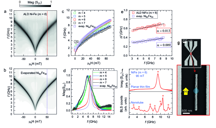
Now we report on the magnetization dynamics of the annealed NiFe samples, investigated by broadband ferromagnetic resonance (FMR) spectroscopy (Figure 7). Figure 7a and b (Figure S6) show the spectra of the evaporated commercial \ceNi80Fe20 thin film and of the PEALD-grown thin films prepared with ( and 7), respectively. The spectra were taken by inductive measurements on a coplanar wave guide (CPW) using a vector network analyzer (VNA) and reflected the magnitude of the scattering parameter . The black branches in the color-coded spectra represent resonant absorption at different values of the in-plane magnetic field. In Figure 7c we compare resonance frequencies for extracted from spectra of the PEALD prepared NiFe thin films and the evaporated permalloy. In Figure 7d we compare the individual spectra taken at the same field of 50 mT for thin films prepared with Ni:Fe pulse ratios and and for the evaporated permalloy thin film used as a reference. The linewidths , extracted from fitting a Lorentzian function to the spectra , were employed to determine the damping parameter of the materials (Methods). In Figure 7e we report as a function of the resonance frequency for the PEALD sample prepared with (upper curve) and the reference permalloy sample (lower curve). The curves are fitted by a linear function, whose slope is twice the damping parameter 57. The extracted values are displayed next to the curves. The value obtained for the ALD-grown thin film is larger than 0.009 detected on the reference NiFe film. The hole like features in the PEALD film most likely induce two-magnon scattering 58, 59 and increase beyond 0.009.
In Figure 7f we show the imaginary component of the scattering parameter measured on a NiFe thin film prepared with by VNA-FMR and compare it with the spectrum obtained by microfocused Brillouin Light Scattering (-BLS) on a nanotube prepared with the same PEALD process. The spectrum was measured at the central position of the NT as depicted in Figure 7g. Both spectra were acquired at = 90 mT. Resonance frequencies are indicated with open red circles.
Figure 7g shows a SEM micrograph of both the coplanar wave guide (CPW) employed to excite the spin precession in the individual NT and the NT parallel to the CPW’s signal line. The blue circle indicates the position of the blue laser employed to detect the excited spin waves modes via -BLS. The direction of the external applied field is indicated with a yellow arrow. The -BLS spectrum of the permalloy NT is much richer than the ones reported for PEALD-prepared nickel nanotubes 46. The series of resonance peaks indicate confined spin waves as previously reported for Ni NTs 46. We attribute the larger number of resolved spin-wave resonances in Figure 7f to the lower damping of NiFe compared to Ni. A detailed discussion about the nature of the additionally observed modes is beyond the scope of this paper.
Our results show that in the case of the Ni:Fe pulse ratio in the ALD deposition process we achieve field-dependent resonance frequencies (Figure 7c) and a Gilbert damping parameter (Figure 7d) which are close to those values measured for a standard permalloy thin film of stoichiometry \ceNi80Fe20. When studying the linewidths of field dependent resonant modes detected locally on the NT by means of -BLS, we determined a Gilbert damping parameter of 0.01 (Figure S7). The -BLS technique allowed, in fact, to focus the laser on a defect-free region of the nanostructure. Thereby extrinsic contributions to the peak broadening were less dominant. The spin-wave spectroscopy confirmed the good quality of the ALD-grown permalloy and its reduced damping compared to ALD-grown Ni 46, opening new possibilities for applications in 3D nanomagnonics.
3 Methods
3.1 Plasma Enhanced Atomic Layer Deposition of NiFe and Subsequent Annealing
Si (100) wafers were cleaved in pieces of about 2 cm x 2 cm and employed as substrates for the deposition of planar NiFe thin films. The Si substrates were cleaned with the following procedure: 15 min in \ceH2O : \ceNH4OH (28) : \ceH2O2 (5:1:1) at 70∘C; 10 s in \ceHF (49) : \ceH2O (1:10) at room temperature; 15 min in \ceH2O : \ceHCl (37) : \ceH2O2 (6:1:1) at 75 ∘C.
GaAs NWs were grown on Si (111) substrates as fully described in references 60, 61 and used as nanotemplates. The Si wafers were used both as bare substrates and coated with a 5 nm - thick layer of ALD alumina (\ceAl2O3) as previously described 46. GaAs NWs were employed pre-coated with alumina. Nickel-Iron growth experiments were performed in a hot wall Beneq TFS 200 ALD reactor, operated at a pressure of 4-5 mbar, under a 100 sccm costant flow of ultrahigh purity nitrogen, used both as carrier and purge gas. We used nickelocene (\ceNiCp2), iron(III) tert-butoxide complex (\ceFe2(OtBu)6) and water as precursors and reactant. They were stored in stainless steel containers at 80∘C, 100∘C and room temperature, respectively, to exploit their vapor pressure. The chamber temperature was set as 170C. The plasma was generated in an RF parallel plate system and powered at 150 W. Pure hydrogen was supplied through the plasma head with a flow rate of 300 sccm. The PEALD sequence can be summarized as follows: [(\ceNiCp2/purge/\ceH2O/purge/\ceH2 plasma/purge) + (\ceFe2(OtBu)6/purge/\ceH2O/purge/\ceH2 plasma/purge)] n. The corresponding steps duration was the following: [(2s/4s/4s/8s/4s/8s) m + (2s/4s/4s/8s/4s/8s)] n . NiFe thin films with thickness of 25 3 nm were prepared setting and 7 and using and 190, respectively, in order to keep the total number of precursors pulses equal to 1500, for each process. The thickness of the deposited thin films was measured by imaging the films in cross section by SEM. The growth rate was calculated by dividing the thickness by the total number of precursors pulses . Thin films prepared on Si, Si / \ceAl2O3 planar substrates and GaAs / \ceAl2O3 NWs were thermally treated at 380∘C for 2h 30 min under forming gas \ceN2 - \ceH2 with flow 300 sccm. This temperature was reported to be sufficient to activate the reduction of iron oxide in the presence of nickel 45.
Reference permalloy thin films were prepared in an electron-beam evaporator Leybold Optics LAB 600H, using a commercial target of \ceNi80Fe20. A 50-nm-thick thin film was used as a reference for comparison in the paper, except for the measurements of resistivity and anisotropic magnetoresistance. Here we employed a reference \ceNi80Fe20 sample with a thickness of 20 nm comparable to the one of annealed NiFe samples prepared by ALD.
3.2 Structural Characterization and Chemical Analysis of the Thin Films and Nanotubes
We report the properties of the annealed thin films. Their morphologies and thicknesses were investigated by scanning electron microscopy (SEM) from Zeiss and Bruker and atomic force microscopy (AFM) from Bruker. Chemical analysis of thin films were performed by SEM combined with energy dispersive X-ray spectroscopy (SEM-EDS) on a Zeiss Merlin system (beam energy: 15 keV). X-ray diffraction spectra were recorded in the glancing incidence mode on a Malvern Panalytical(Empyrean model) diffractometer with incidence angle of 0.8∘. The morphologies of the annealed nanotubes was investigated by both SEM and transmission electron microscopy (TEM), chemical element distribution was examined by scanning transmission electron microscopy (STEM) combined with energy dispersive X-ray spectroscopy (STEM-EDS). The TEM and STEM experiments were carried out using an FEI Talos electron microscope operated at 200 kV. The thicknesses of the NTs were extracted from EDS elemental 2D maps of Ga and Ni using the software Velox, as previously discussed 46. The diffraction pattern was simulated using the software JEMS, for the Ni:Fe crystal structure with atomic ratio 75:25.
3.3 Investigation of Physical Properties of Thin Films
The static magnetic properties of the thin films were assessed using a Microsense EZ-7 vibrating sample magnetometer (VSM) operated at room temperature. The saturation magnetization values were determined from the VSM hysteresis by normalizing the magnetization M (emu) measured at 150 mT by the volume of the material Vm. For the calculation of Vm the estimated volume of holes measured by AFM has been substracted. Resistivity measurements were performed with a KLA Tencor OmniMap RS75 four-point resistivity meter. Anisotropic magnetoresistance (AMR) measurements were carried out in the van der Pauw four-point configuration 62 in a custom-built set-up described previously 46. AMR measurements were performed at room temperature applying a current of 10 A and a static in-plane magnetic field of 80 mT applied at an angle varying from 0 to 360∘. Broadband spectroscopy of the deposited thin films was performed using a vector network analyzer (VNA), sweeping the frequency and recording the ferromagnetic resonance (FMR) absorption spectra. The thin films were positioned on top of a CPW connected by microwave tips to the VNA. The 2-port VNA generates a microwave current providing an in-plane rf-magnetic field perpendicular to the long axis of the CPW. The frequency of the microwave magnetic field was swept from 10 MHz to 15 GHz. The microwave with a power of dBm was applied at port 1 of the CPW in order to excite magnetization precession. The precession-induced voltage was detected at port 2 via the scattering parameter where the numbers 2 and 1 in the subscript denote the detection and excitation port. An external magnetic field was swept from 90 mT to mT along the CPW’s long axis. The field dependent frequency behavior was assessed by fitting the data by the Kittel equation 56, 57. The Gilbert damping parameter was determined by plotting the linewidth against the corresponding resonance frequencies. The curve was fitted by a linear function, whose slope is twice the damping parameter . The of the imaginary component of the scattering parameter was estimated dividing by the linewidth of the magnitude component of (f Mag)7. The metallic coplanar wave guide (CPW) for the investigation of the NT was fabricated by electron beam lithography and a following evaporation of 5 nm Ti/ 120 nm Au film. The signal line, having a width of 2.5 0.1 m was separated by gaps of 1.7 0.1m width from the ground lines. The CPW was fabricated around individual NTs placed parallel to the signal line and electrically bonded to a printed circuit board, which was connected to a signal generator (Anritsu MG3692C) applying a microwave current. The corresponding magnetic microwave field excited spin precession in the NT at a fixed frequency. Spin wave eigenmodes were detected via microfocused Brillouin light scattering (-BLS) microscopy at room temperature 63. A monochromatic blue laser with a wavelength of 473 nm and power of 0.5 mW was focused directly on top of the NT.
4 Conclusions
NiFe thin films with different Ni:Fe atomic ratios were prepared by alternating times the sequence for the deposition of nickel with a single sequence for the deposition of oxidized iron and a post-deposition annealing treatment in hydrogen. We achieved an optimized stoichiometry via the Ni:Fe pulse ratio . By a further annealing step the resistivity of the optimized permalloy (Py) thin films was 28 cm and the measured spin wave damping 0.013. A high relative AMR of 5.6 was observed in the ALD-grown Py thin film with lowest spin wave damping. The high quality of the films allowed us to measure multiple resonant spin-wave eigenmodes in an individual Py nanotube. In the case of Py NTs the spectra were richer compared to the previously reported ALD-grown Ni NTs substantiating the lower damping of Py. The permalloy thin films and nanotubes thereby exhibited physical properties that make them promising for functional spintronic elements and magnonic applications in 3D device architectures.
Conflicts of interest
There are no conflicts to declare.
Acknowledgements
We thank SNF for funding our research via grants 163016, BSCGI0_157705, NCCR QSIT and 197360. We thank Didier Bouvet, Bi Wen Hua and Ivica Zivkovic for the excellent experimental support.
Notes and references
- Kryder 1992 M. H. Kryder, Thin Solid Films, 1992, 216, 174 – 180.
- Lenz and Edelstein 2006 J. Lenz and S. Edelstein, IEEE Sensors Journal, 2006, 6, 631–649.
- Kools 1996 J. C. S. Kools, IEEE Transactions on Magnetics, 1996, 32, 3165–3184.
- Niarchos 2003 D. Niarchos, Sensors and Actuators A: Physical, 2003, 106, 255 – 262.
- Venkateshwaran et al. 2019 S. Venkateshwaran, E. Selvakumar, P. Senthamil selvan, M. Selvambikai, R. Kannan and A. S. Pradeep, Advances in Materials and Metallurgy, 2019, pp. 447–454.
- Parkin et al. 2008 S. S. P. Parkin, M. Hayashi and L. Thomas, Science, 2008, 320, 190–194.
- Neusser and Grundler 2009 S. Neusser and D. Grundler, Adv. Mater., 2009, 21, 2927–2932.
- Kruglyak et al. 2010 V. V. Kruglyak, S. O. Demokritov and D. Grundler, J. Phys. D: Appl. Phys., 2010, 43, 264001.
- Nikitov et al. 2015 S. A. Nikitov, D. V. Kalyabin, I. V. Lisenkov, A. Slavin, Y. N. Barabanenkov, S. A. Osokin, A. V. Sadovnikov, E. N. Beginin, M. A. Morozova, Y. A. Filimonov, Y. V. Khivintsev, S. L. Vysotsky, V. K. Sakharov and E. S. Pavlov, Physics-Uspekhi, 2015, 58, 1002–1028.
- Stancil and Prabhakar 2009 D. Stancil and A. Prabhakar, Spin Waves: Theory and Applications, Springer, 2009.
- Gubbiotti 2019 G. Gubbiotti, Three-Dimensional Magnonics: Layered, Micro-and Nanostructures; 1st ed, Jenny Stanford Publishing., 2019.
- Wang et al. 2013 S. Wang, T. Gao, C. Wang and J. He, Journal of Alloys and Compounds, 2013, 554, 405 – 407.
- Ohtake et al. 2012 M. Ohtake, Y. Nonaka and M. Futamoto, IEEE Transactions on Magnetics, 2012, 48, 1589–1592.
- Ohtake et al. 2011 M. Ohtake, T. Tanaka, K. Matsubara, F. Kirino and M. Futamoto, Journal of Physics: Conference Series, 2011, 303, 012015.
- Tabakovic et al. 2014 I. Tabakovic, J. Gong, S. Riemer and M. Kautzky, Journal of The Electrochemical Society, 2014, 162, D102–D108.
- Balachandran et al. 2009 R. Balachandran, H. Yow, B. Ong, R. Manickam, V. Saaminathan and K. Tan, Journal of Alloys and Compounds, 2009, 481, 336 – 339.
- de la Torre Medina et al. 2018 J. de la Torre Medina, T. da Câmara Santa Clara Gomes, Y. G. Velázquez Galván and L. Piraux, Sci. Rep., 2018, 8, 14555.
- Białostocka et al. 2018 A. Białostocka, U. Klekotka and B. Kalska-Szostko, Chemical Engineering Communications, 2018, 206, 804–814.
- Cortes et al. 2014 M. Cortes, J. Moulin, M. Couty, T. Peng, O. Garel, T. H. N. Dinh, Y. Zhu, M. Souadda, M. Woytasik and E. Lefeuvre, ECS Transactions, 2014, 58, 41–53.
- Pancaldi et al. 2019 M. Pancaldi, N. Leo and P. Vavassori, Nanoscale, 2019, 11, 7656–7666.
- Bhat et al. 2020 V. S. Bhat, S. Watanabe, K. Baumgaertl, A. Kleibert, M. A. W. Schoen, C. A. F. Vaz and D. Grundler, Phys. Rev. Lett., 2020, 125, 117208.
- Sahoo et al. 2018 S. Sahoo, S. Mondal, G. Williams, A. May, S. Ladak and A. Barman, Nanoscale, 2018, 10, 9981–9986.
- Fischer et al. 2020 P. Fischer, D. Sanz-Hernández, R. Streubel and A. Fernández-Pacheco, APL Materials, 2020, 8, 10701.
- Otálora et al. 2017 J. A. Otálora, M. Yan, H. Schultheiss, R. Hertel and A. Kákay, Phys. Rev. B, 2017, 95, 184415.
- Streubel et al. 2016 R. Streubel, P. Fischer, F. Kronast, V. P. Kravchuk, D. D. Sheka, Y. Gaididei, O. G. Schmidt and D. Makarov, J. Phys. D: Appl. Phys., 2016, 49, 363001.
- Yan et al. 2011 M. Yan, C. Andreas, A. Kákay, F. García-Sánchez and R. Hertel, Appl. Phys. Lett., 2011, 99, 122505.
- Fernández-Pacheco et al. 2017 A. Fernández-Pacheco, R. Streubel, O. Fruchart, R. Hertel, P. Fischer and R. P. Cowburn, Nat. Commun., 2017, 8, 15756.
- Landeros et al. 2007 P. Landeros, S. Allende, J. Escrig, E. Salcedo, D. Altbir and E. E. Vogel, Appl. Phys. Lett., 2007, 90, 102501.
- Escrig et al. 2007 J. Escrig, P. Landeros, D. Altbir, E. Vogel and P. Vargas, Journal of Magnetism and Magnetic Materials, 2007, 308, 233 – 237.
- Johnson et al. 2014 R. W. Johnson, A. Hultqvist and S. F. Bent, Mater. Today, 2014, 17, 236–246.
- Oviroh et al. 2019 P. O. Oviroh, R. Akbarzadeh, D. Pan, R. A. M. Coetzee and T.-C. Jen, Science and Technology of Advanced Materials, 2019, 20, 465–496.
- Ritala and Niinistö 2009 M. Ritala and J. Niinistö, ECS Transactions, 2009, 25, 641–652.
- Lim et al. 2003 B. S. Lim, A. Rahtu and R. G. Gordon, Nat. Mater., 2003, 2, 749–754.
- Wang et al. 2016 Y. P. Wang, Z. J. Ding, Q. X. Liu, W. J. Liu, S. J. Ding and D. W. Zhang, J. Mater. Chem. C, 2016, 4, 11059–11066.
- Klesko et al. 2016 J. P. Klesko, M. M. Kerrigan and C. H. Winter, Chemistry of Materials, 2016, 28, 700–703.
- Kerrigan et al. 2018 M. M. Kerrigan, J. P. Klesko, K. J. Blakeney and C. H. Winter, ACS Appl. Mater. Interf., 2018, 10, 14200–14208.
- Hagen et al. 2019 D. J. Hagen, M. E. Pemble and M. Karppinen, Appl. Phys. Rev., 2019, 6, 041309.
- Daub et al. 2007 M. Daub, M. Knez, U. Goesele and K. Nielsch, J. Appl. Phys., 2007, 101, 09J111.
- Rüffer et al. 2012 D. Rüffer, R. Huber, P. Berberich, S. Albert, E. Russo-Averchi, M. Heiss, J. Arbiol, A. Fontcuberta i Morral and D. Grundler, Nanoscale, 2012, 4, 4989–4995.
- Buchter et al. 2013 A. Buchter, J. Nagel, D. Rüffer, F. Xue, D. P. Weber, O. F. Kieler, T. Weimann, J. Kohlmann, A. B. Zorin, E. Russo-Averchi, R. Huber, P. Berberich, A. Fontcuberta i Morral, M. Kemmler, R. Kleiner, D. Koelle, D. Grundler and M. Poggio, Phys. Rev. Lett., 2013, 111, 067202.
- Weber et al. 2012 D. P. Weber, D. Rüffer, A. Buchter, F. Xue, E. Russo-Averchi, R. Huber, P. Berberich, J. Arbiol, A. Fontcuberta i Morral, D. Grundler and M. Poggio, Nano Lett., 2012, 12, 6139–6144.
- Rüffer et al. 2014 D. Rüffer, M. Slot, R. Huber, T. Schwarze, F. Heimbach, G. Tütüncüoglu, F. Matteini, E. Russo-Averchi, A. Kovács, R. Dunin-Borkowski, R. R. Zamani, J. R. Morante, J. Arbiol, A. Fontcuberta i Morral and D. Grundler, APL Mater., 2014, 2, 076112.
- Huber 2013 R. Huber, Ph.D. thesis, Munich University of Technology, 2013.
- Chong et al. 2010 Y. T. Chong, E. M. Y. Yau, K. Nielsch and J. Bachmann, Chemistry of Materials, 2010, 22, 6506–6508.
- Espejo et al. 2016 A. P. Espejo, R. Zierold, J. Gooth, J. Dendooven, C. Detavernier, J. Escrig and K. Nielsch, Nanotechnology, 2016, 27, 345707.
- Giordano et al. 2020 M. C. Giordano, K. Baumgaertl, S. Escobar Steinvall, J. Gay, M. Vuichard, A. Fontcuberta i Morral and D. Grundler, ACS Applied Materials & Interfaces, 2020, 12, 40443–40452.
- Chae et al. 2002 J. Chae, H. S. Park and S. W. Kang, Electrochem. Solid-State Lett., 2002, 5, C64.
- Bachmann et al. 2007 J. Bachmann, J. Jing, M. Knez, S. Barth, H. Shen, S. Mathur, U. Gösele and K. Nielsch, J. Am. Chem. Soc., 2007, 129, 9554–9555.
- Escrig et al. 2008 J. Escrig, J. Bachmann, J. Jing, M. Daub, D. Altbir and K. Nielsch, Phys. Rev. B, 2008, 77, 214421.
- Bachmann et al. 2009 J. Bachmann, J. Escrig, K. Pitzschel, J. M. Moreno, J. Jing, D. Görlitz, D. Altbir and K. Nielsch, J. Appl. Phys., 2009, 105, 07B521.
- Vernyhora et al. 2012 I. Vernyhora, V. Tatarenko and S. Bokoch, ISRN Thermodynamics, 2012, 2012, Article ID 917836 (11pp).
- Glaubitz et al. 2011 B. Glaubitz, S. Buschhorn, F. Brüssing, R. Abrudan and H. Zabel, Journal of Physics: Condensed Matter, 2011, 23, 254210.
- Gao et al. 1997 L. J. Gao, P. Ma, K. M. Novogradecz and P. R. Norton, Journal of Applied Physics, 1997, 81, 7595–7599.
- Yin et al. 2006 L. F. Yin, D. H. Wei, N. Lei, L. H. Zhou, C. S. Tian, G. S. Dong, X. F. Jin, L. P. Guo, Q. J. Jia and R. Q. Wu, Phys. Rev. Lett., 2006, 97, 067203.
- McGuire and Potter 1975 T. McGuire and R. Potter, IEEE Transactions on Magnetics, 1975, 11, 1018–1038.
- Kittel 1948 C. Kittel, Phys. Rev., 1948, 73, 155–161.
- Gurevich and Melkov 1996 A. G. Gurevich and G. A. Melkov, Magnetization oscillations and waves, CRC Press, Boca Raton, 1996.
- Tserkovnyak et al. 2005 Y. Tserkovnyak, A. Brataas, G. E. Bauer and B. I. Halperin, Rev. Mod. Phys., 2005, 77, 1375–1421.
- Arias and Mills 1999 R. Arias and D. L. Mills, Phys. Rev. B, 1999, 60, 7395–7409.
- Matteini et al. 2015 F. Matteini, V. G. Dubrovskii, D. Rüffer, G. Tütüncüoğlu, Y. Fontana and A. Fontcuberta i Morral, Nanotechnology, 2015, 26, 105603.
- Matteini et al. 2016 F. Matteini, G. Tütüncüoglu, D. Mikulik, J. Vukajlovic-Plestina, H. Potts, J.-B. Leran, W. C. Carter and A. Fontcuberta i Morral, Crystal Growth & Design, 2016, 16, 5781–5786.
- Kateb et al. 2019 M. Kateb, E. Jacobsen and S. Ingvarsson, J. Phys. D: Appl. Phys., 2019, 52, 075002.
- Demokritov 2008 V. E. Demokritov, S. O. Demidov, IEEE Trans. Magn., 2008, 44, 6–12.
See pages - of SupplinfoArxiv.pdf