Unveiling the dopant segregation effect at hematite interfaces
Abstract
Understanding the effects of atomic structure modification in hematite photoanodes is essential for the rational design of high-efficiency functionalizations. Recently it was found that interface modification with Sn/Sb segregates considerably increases hematite photocatalytic efficiency. However, the understanding of the different electronic effects of these modifications at the atomic level is still lacking. This letter describes the segregation effects of two different dopants—Sn and Sb—on both the solid-solid (grain-boundaries) and solid-liquid interfaces (surfaces) of hematite. Within an ab initio approach, we quantitatively extract the potential barrier reduction on polycrystalline interfaces due to the dopant, which causes an increase in the inter-grain electron transport. Concomitantly, the dopants’ segregation on hematite surfaces results in a decrease of the oxygen vacancy formation energy. Such vacancies lead to the experimentally observed rise of the flat-band potential. The comprehension of the electronic effects of dopants on both types of interfaces explains the experimental peak efficiency of interface-modified hematite with dopant segregates, also enabling the control and design of interfaces for different higher-efficiency applications.
Hematite (-Fe2O3), an n-type semiconductor with high photoelectrochemical stability, is considered the most promising material to be used as a photoanode for water splitting (with a potential to convert of the sun’s energy into hydrogen) [1]. However, problems related to low electronic conductivity and poor kinetics of charge transfer (mainly holes) at the semiconductor-liquid interface causes an efficiency in the water oxidation process far below the theoretical prediction [2]. An alternative found to overcome these problems on hematite is the insertion of metallic and semi-metallic elements, such as Sn and Sb [3, 4, 5, 6].
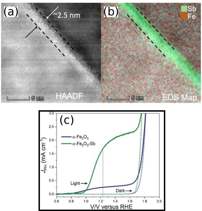
The ionic nature of hematite – which is associated with Schottky intrinsic ionic disorder – leads to dopants segregation at grain boundaries and free surfaces [7, 8]. Consequently, the physical-chemistry structure of the solid-solid (grain boundary in a polycrystalline film) and solid-liquid interfaces is modified. Recently, the addition of Sn on hematite was shown to preferentially segregate at the grain boundary region [9]. Similarly, sintered hematites with by weight of Sb2O3 also leads to Sb segregation at the grain boundary region [6]. The scanning transmission electron microscopy (STEM) with high angle annular dark-field (HAADF) image [Fig. 1(a)], as well as the energy-dispersive spectroscopy [EDS Map, Fig. 1(b)] show a Sb layer of approximately nm thick. Both dopants segregating at grain boundary region shows a reduction in total electronic resistivity, with a specific decrease in the grain boundary resistance [9, 10]. Sn or Sb promotes a decrease of 3 to 5 orders of magnitude in the electronic resistivity on hematite [9, 10]. The dopant segregation also modifies the solid-liquid interfaces, changing the photoelectrochemical properties of hematite photoanodes [3, 6]. Indeed, as illustrated in Fig. 1(c), the addition of Sb promotes a significant increase in photocurrent (). Moreover, an increase in the flat band potential () is also reported, suggesting the formation of surface states [6]. The Sn doped hematite shows similar results, i.e., an increase in and [3].
Despite efforts dedicated to understanding the role of dopants from macroscopic to atomic-scale analysis — revealing the atomic scale segregation at the hematite interfaces leading to those discussed effects — a profound lack of information remains regarding its electronic structure. This letter is devoted to unravelling how the electronic structure is affected by dopant segregation at hematite interfaces — assigned by decreasing the grain boundary resistance, with the concomitant creation of surface states at the solid-liquid interface. By employing density functional theory (DFT) calculations, we describe the electronic effects of Sb/Sn-doped hematite surfaces and grain boundaries. Here we have shown that the favorable conditions for O-vacancy formation in the doped surfaces rule the flat-band potential increase. By tracking the effective electronic potential across hematite grain-boundaries, we predict the decrease of the effective potential barrier height, increasing the electron transport rate between grains.
Methods. DFT calculations [11, 12, 13] are performed using the Viena Ab-initio Simulation Package (VASP) implementation [14]. The exchange-correlation term was described using the GGA functional proposed by Perdew, Burke, and Ernzerhof (PBE) [15, 16]. The Kohn-Sham orbitals are expanded in a plane wave basis set with an energy cutoff of eV. The electron-ion interactions are taken into account using the Projector Augmented Wave (PAW) method [17]. All geometries have been relaxed until the atomic forces were lower than eV/Å. The Brillouin Zone (BZ) is sampled according to the Monkhorst-Pack method [18], using a gamma-centered mesh for atomic structure relaxation and a mesh for obtaining the self-consistent total charge density for the bulk calculations. The slab and grain-boundary (GB) calculations were performed with the same k-mesh, but with a single k-point in the confined directions. In the slab calculations a vacuum region of at least 12 Å was considered in order to avoid spurious interactions between periodic images. To describe the Fe orbitals’ strong Coulomb interaction, we have considered the on-site repulsion term with eV [19], which has shown to represent hematite magnetic phase and energy gap correctly [20].
Hematite surface electronic structure. Concomitantly with the segregation of Sn/Sb atoms on hematite GB, upon sample preparations, Sn/Sb modified surfaces are present in the solid-liquid interface [9, 6]. Previous studies attributed this modification as responsible for the increase of , Figure 1(c). By looking at different hematite surfaces, we can extract the effect of Sn/Sb on the system Fermi level in relation to the water redox potential () and thus discuss the flat band potential variation.
Keeping the stoichiometry of the bulk we cleave the Hematite in the [001], [100] and [110] directions, and their surface energies,
| (1) |
were computed; with and the total energies of the slab and bulk calculations, respectively; is the slab/bulk fraction of atoms; and is the slab area. Here we find , , and J/cm2, for the (001), (100), and (110) surfaces, respectively. Therefore there is a lower cleavage energy for the (110) surface. Such preference for the (110) surface has also been experimentally verified [21, 22]. As a study case we have focused in the two lowest energy surfaces (001) and (110) to consider the Sn/Sb segregation effects.
We have considered the Sn/Sb atoms to enter substitutionally at the energetic more favorable top-most surface Fe sites [23], in three possible surface terminations: stoichiometric, O-vacancy, and O-rich. The substitutional doping formation energy is negative indicating an exothermic process for the O-poor termination with eV/Sb and eV/Sn; in contrast for the surfaces with higher O concentration (stoichiometricO-rich), the formation energy become positive with eV/Sb and eV/Sn. Such doped formation energy values on the surface are lower than the calculated on the hematite bulk, eV/Sb and eV/Sn, which corroborates the experimentally observed surface doping.
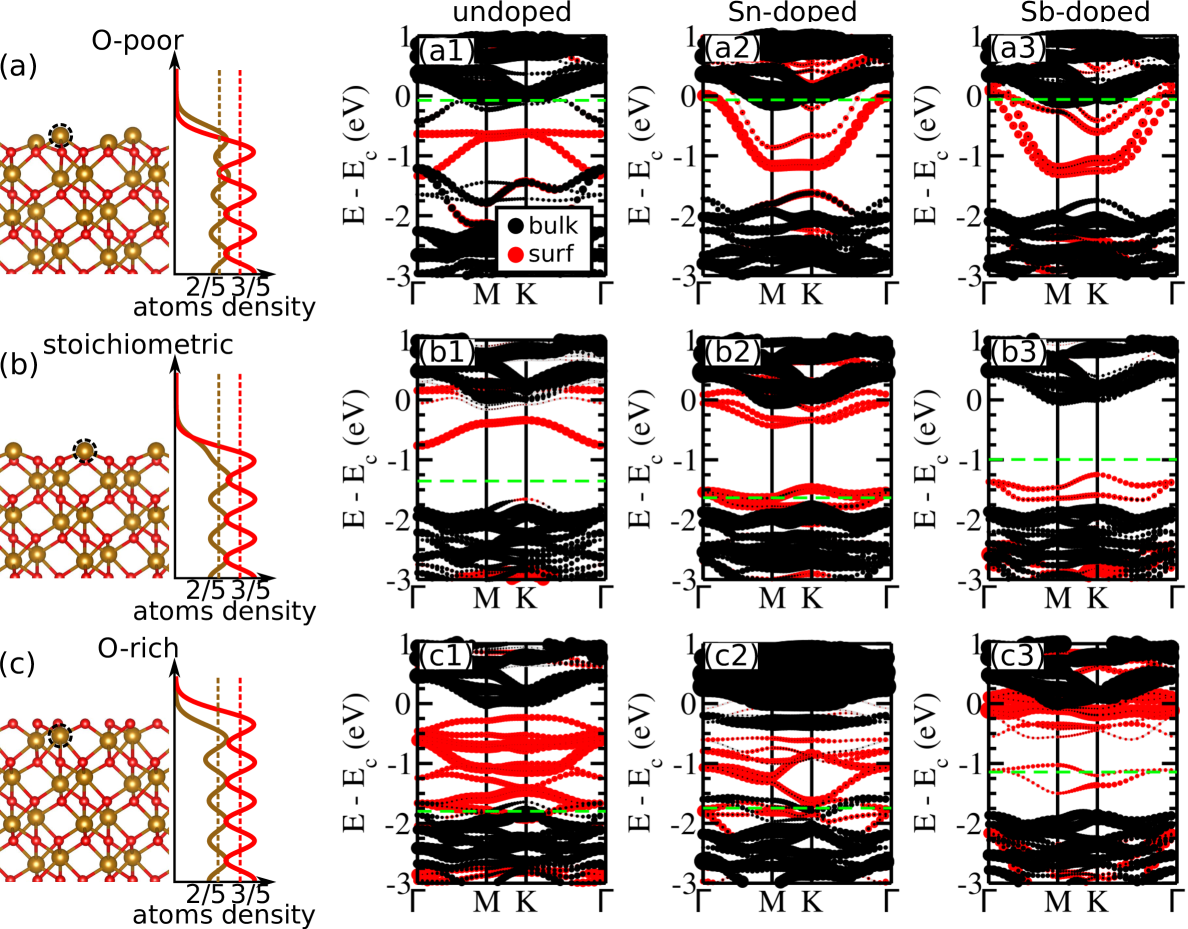
From the electronic point of view, in the stoichiometric case, the foreign atoms enter the Fe3+ sites with oxidation states Sn4+ and Sb5+. Meanwhile, upon the presence of neighboring oxygen vacancies, the oxidation states change to Fe2+, Sn2+, and Sb3+. Despite the modification of the oxidation states in the presence of oxygen vacancies, the surface incorporation of Sb/Sn has little effect on the Fermi level position with respect to the hematite bulk VBM and CBM. In Fig. 2 we show the projected band structure for the (001) surface, with the slab interior (bulk states) contribution displayed in black, and the surface states contribution in red. We can see that the surface termination rules the Fermi level shift. For instance, we see the Fermi level (green dashed line) of the stoichiometric and O-rich slab termination close to the valence band for all doping cases [Fig. 2(b) and (c)]. However, for O-poor termination, there is an upshift of the Fermi level towards the conduction band [Fig. 2(a)]. In all studied cases, surface states (red circles) are present on the hematite bulk bandgap. Such a situation allows us to establish the picture show in Figure 3.
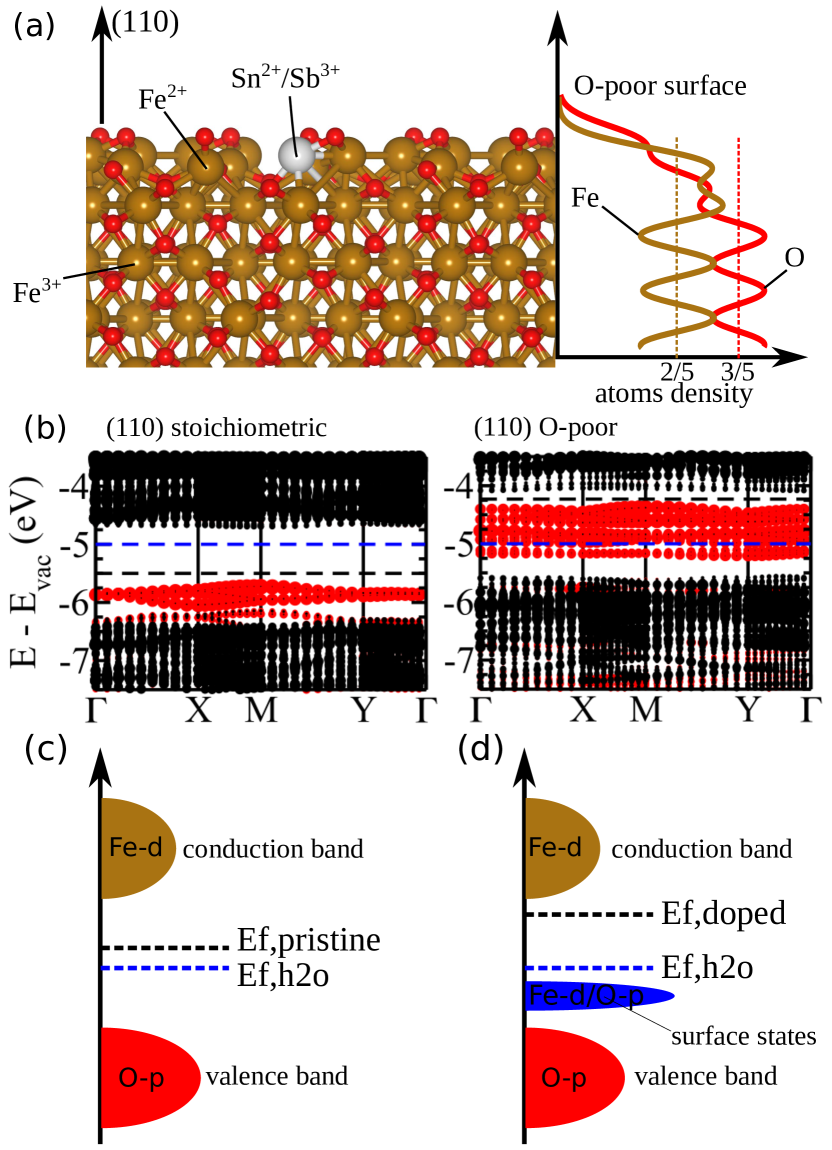
In the stoichiometric terminations, the Fermi level remains in the hematite bulk bandgap. In Fig. 3(b) left panel, we have shown the stoichiometric (110) terminated slab band structure, with the system Fermi level (black dashed line) within the valence/conduction energy gap of the bulk states (black circles). Experimentally it is known that hematite is an n-doped semiconductor [1], presenting the scenario shown in Fig. 3(c). Upon the formation of O-vacancy on the surface [Figure 3(a)], the is shifted towards the bulk conduction band [Fig. 3(b) right panel], leading to the increase in [Figure 3(d)]. Since the oxygen in hematite is , its vacancy act as an n-dopant. The reciprocal is true for the O-rich surface, where the Fermi level shifts towards the bulk valence band, Fig. 2(c). We see surface states, ruled by the Fe- and O- orbitals hybridization, appearing within the bulk energy gap in all slab calculations, which can serve as hole traps [24]. This prediction goes according to recent experiments where NiFeOx act passivating those surface states, where the pristine character of the surface has been restored by the suppression of the hole traps [25].
Although Sn/Sb surface modification appears to have no direct effect on the surface Fermi energy, we see a reduction of O-vacancy formation energy by eV and eV, in the presence of Sn and Sb, respectively. Therefore we can establish the picture of increased O-vacancy formation, ruled by the presence of Sn in the hematite surface. Such lowering of the vacancy formation on hematite surface leads to the over-potential [26] and complete previous studies of O-vacancy facilitation on the bulk by the presence of Ti or Sn dopants [27].
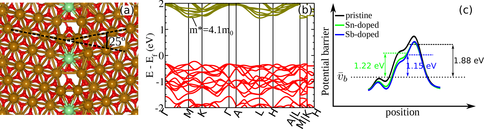
Sn/Sb doped grain boundaries. Experiments undoubtedly predicted that hematite photocurrents undergo a transition from one grain to the other rather than percolating along the grain boundaries [9]. Such claims, concomitantly with the observation of increased photocurrent upon atoms’ segregation at the GB, currently lack microscopic evidence. By constructing hematite grain boundaries, Fig. 4(a), we track the electron potential barrier evolution by incorporating foreign Sn and Sb atoms at the GB 111The generated GB cell considers two grains rotated by 25o with respect to each other, with two GBs in the unit cell to guarantee the periodicity, with 13.4 Å of lateral separation. Our choice were guided by experimental results, which show that hematice grain boundaries present high-angles [9], with most of it higher than 15o [31]. We have constructed the lowest possible commensurate angle which was still computationally viable, hosting 284 atoms in the unit cell.. From Figure 4(a) we see a lower atomic concentration at the GB, compared with the pristine region of the grain, consistent with experimental HAADF images [9]. By substituting a Fe atom by Sn/Sb in the GB region [green atom in Fig. 4(a)], i.e., keeping the same atomic concentration, we see a reduction of the effective potential energy barrier, Fig. 4(c). Such reduction can be understood by the lower potential energy () of the higher effective atomic number () of Sn and Sb. We can estimate a quantitative effect of this reduction on the electron transport across the GB, approximating a rectangular barrier’s potential profile. Here the barrier width is Å, and the height goes from eV to eV ( eV), relative to the bulk mean potential (), upon Sn/Sb segregation. In this effective free electron approximation, the wave-vector reads , with the electron kinetic energy. We have calculated the conduction band minimum (CBM) effective mass to be [Fig. 4(b)], close to previous studies [29] and experimental estimations [30]. For a rectangular barrier, the transmission coefficient is written as
| (2) |
where the , and represents the pristine and doped GB, respectively. In this approximation we predict that the electron transmission increases upon Sn (Sb) doping by a factor of () for lower kinetic energy (), and both going towards for higher electron kinetic energy (). The observed photocurrent can be statically viewed as , with the photon absorption crossection (electron-hole pair generation), the electron-hole recombination rate, the electron charge and the drift velocity of the electrons in the material. The drift velocity is dependent on the materials conductivity and the bias between the electrodes, . For a polycrystaline material with non-percolating grains transport, as in hematite [9], the conductivity () depends directly on the tunneling rate between grains. Therefore, the photocurrent is proportional to the transmission rate of the electrons between grains. Astonishingly, the experimental increase of the photocurrent occurs by a factor of for Sn doped [25] and for Sb doped [6], at the same order of the values predicted by our approximated model. Such microscopic interpretation allows us to understand and predict quite reasonably the experimentally observed increase of the photocurrent upon Sn/Sb doping.
In summary, we have presented a clear picture of the dopants segregation effect on the solid-solid and solid-liquid interfaces of hematite. We show that in hematite’s grain boundaries (solid-solid interface), the Sn/Sb dopants reduce the electronic barrier, increasing the inter-grain electron transmission. Our results predict that the segregation of other dopants with higher atomic numbers will also contribute to the photocurrent increase. On the other hand, the dopants’ effect on the hematite’s surface (solid-liquid interface) electronic is indirect. The Sn/Sb dopants lower the oxygen vacancy formation, leading to the flat band potential increase. Our results describing the electronic effects of segregation can guide the rational functionalization of hematite towards higher-efficiency photoanodes.
ACKNOWLEDGMENTS
The authors acknowledge financial support from FAPESP (projects CEPID - 2013/07296-2, 2017/03135, 17/18139-6, 17/02317-2, 2018/05159-1 and 2019/20857-0), FINEP, CNPq (project 401452/2017-4, process 168295/2017-2), and CAPES (grand numbers 88887.310931/2018-00 and 88882.332718/2019–01). The authors also acknowledge the Laboratório Nacional de Computação Científica (project SCAFMat2) for computer time.
Data Availability Statement
The data that support the findings of this study are available from the corresponding author upon reasonable request
References
- Sivula, Le Formal, and Grätzel [2011] K. Sivula, F. Le Formal, and M. Grätzel, “Solar Water Splitting: Progress Using Hematite (-Fe2O3) Photoelectrodes,” ChemSusChem 4, 432–449 (2011).
- Walter et al. [2010] M. G. Walter, E. L. Warren, J. R. McKone, S. W. Boettcher, Q. Mi, E. A. Santori, and N. S. Lewis, “Solar Water Splitting Cells,” Chemical Reviews 110, 6446–6473 (2010).
- Gonçalves and Leite [2014] R. H. Gonçalves and E. R. Leite, “The colloidal nanocrystal deposition process: an advanced method to prepare high performance hematite photoanodes for water splitting,” Energy Environ. Sci. 7, 2250–2254 (2014).
- Hufnagel et al. [2018] A. G. Hufnagel, H. Hajiyani, S. Zhang, T. Li, O. Kasian, B. Gault, B. Breitbach, T. Bein, D. Fattakhova-Rohlfing, C. Scheu, and R. Pentcheva, “Why Tin-Doping Enhances the Efficiency of Hematite Photoanodes for Water Splitting—The Full Picture,” Advanced Functional Materials 28, 1804472 (2018).
- Annamalai et al. [2018] A. Annamalai, R. Sandström, E. Gracia-Espino, N. Boulanger, J.-F. Boily, I. Mühlbacher, A. Shchukarev, and T. Wagberg, “Influence of Sb5+ as a Double Donor on Hematite (Fe3+) Photoanodes for Surface-Enhanced Photoelectrochemical Water Oxidation,” ACS Applied Materials & Interfaces 10, 16467–16473 (2018).
- Nogueira et al. [2019] A. E. Nogueira, M. R. Santos Soares, J. B. Souza Junior, C. A. Ospina Ramirez, F. L. Souza, and E. R. Leite, “Discovering a selective semimetal element to increase hematite photoanode charge separation efficiency,” J. Mater. Chem. A 7, 16992–16998 (2019).
- Soares et al. [2016] M. R. S. Soares, R. H. Gonçalves, I. C. Nogueira, J. Bettini, A. J. Chiquito, and E. R. Leite, “Understanding the fundamental electrical and photoelectrochemical behavior of a hematite photoanode,” Phys. Chem. Chem. Phys. 18, 21780–21788 (2016).
- Engel and Tuller [2014] J. Engel and H. L. Tuller, “The electrical conductivity of thin film donor doped hematite: from insulator to semiconductor by defect modulation,” Phys. Chem. Chem. Phys. 16, 11374–11380 (2014).
- Soares et al. [2019] M. R. S. Soares, C. A. R. Costa, E. M. Lanzoni, J. Bettini, C. A. O. Ramirez, F. L. Souza, E. Longo, and E. R. Leite, “Unraveling the Role of Sn Segregation in the Electronic Transport of Polycrystalline Hematite: Raising the Electronic Conductivity by Lowering the Grain-Boundary Blocking Effect,” Advanced Electronic Materials 5, 1900065 (2019).
- Destro [2020] F. B. Destro, Number of grain and its influence on electrical properties of hematite modified with different cations, Ph.D. thesis, Departament of Materials Science and Engineering, Federal University of São Carlos (2020).
- Hohenberg and Kohn [1964] P. Hohenberg and W. Kohn, “Inhomogeneous electron gas,” Phys. Rev. 136, B864–B871 (1964).
- Kohn and Sham [1965] W. Kohn and L. J. Sham, “Self-consistent equations including exchange and correlation effects,” Phys. Rev. 140, A1133–A1138 (1965).
- Schleder et al. [2019] G. R. Schleder, A. C. M. Padilha, C. M. Acosta, M. Costa, and A. Fazzio, “From DFT to machine learning: recent approaches to materials science–a review,” Journal of Physics: Materials 2, 032001 (2019).
- Kresse and Furthmüller [1996] G. Kresse and J. Furthmüller, “Efficiency of ab-initio total energy calculations for metals and semiconductors using a plane-wave basis set,” Computational Materials Science 6, 15 – 50 (1996).
- Perdew, Burke, and Ernzerhof [1996] J. P. Perdew, K. Burke, and M. Ernzerhof, “Generalized Gradient Approximation Made Simple,” Phys. Rev. Lett. 77, 3865–3868 (1996).
- Perdew, Burke, and Ernzerhof [1997] J. P. Perdew, K. Burke, and M. Ernzerhof, “Generalized Gradient Approximation Made Simple [Phys. Rev. Lett. 77, 3865 (1996)],” Phys. Rev. Lett. 78, 1396–1396 (1997).
- Blöchl [1994] P. E. Blöchl, “Projector augmented-wave method,” Phys. Rev. B 50, 17953–17979 (1994).
- Monkhorst and Pack [1976] H. J. Monkhorst and J. D. Pack, “Special points for Brillouin-zone integrations,” Phys. Rev. B 13, 5188–5192 (1976).
- Dudarev et al. [1998] S. L. Dudarev, G. A. Botton, S. Y. Savrasov, C. J. Humphreys, and A. P. Sutton, “Electron-energy-loss spectra and the structural stability of nickel oxide: An LSDA+U study,” Phys. Rev. B 57, 1505–1509 (1998).
- Huang, Ramadugu, and Mason [2016] X. Huang, S. K. Ramadugu, and S. E. Mason, “Surface-Specific DFT + U Approach Applied to -Fe2O3(0001),” The Journal of Physical Chemistry C 120, 4919–4930 (2016).
- Kay, Cesar, and Grätzel [2006] A. Kay, I. Cesar, and M. Grätzel, “New Benchmark for Water Photooxidation by Nanostructured -Fe2O3 Films,” Journal of the American Chemical Society 128, 15714–15721 (2006).
- Wen et al. [2005] X. Wen, S. Wang, Y. Ding, Z. L. Wang, and S. Yang, “Controlled Growth of Large-Area, Uniform, Vertically Aligned Arrays of -Fe2O3 Nanobelts and Nanowires,” The Journal of Physical Chemistry B 109, 215–220 (2005).
- Ling et al. [2011] Y. Ling, G. Wang, D. A. Wheeler, J. Z. Zhang, and Y. Li, “Sn-doped hematite nanostructures for photoelectrochemical water splitting,” Nano Letters 11, 2119–2125 (2011).
- Wang et al. [2019] Z. Wang, X. Mao, P. Chen, M. Xiao, S. A. Monny, S. Wang, M. Konarova, A. Du, and L. Wang, “Understanding the Roles of Oxygen Vacancies in Hematite-Based Photoelectrochemical Processes,” Angewandte Chemie International Edition 58, 1030–1034 (2019).
- Freitas et al. [2020] A. L. M. Freitas, D. N. F. Muche, E. R. Leite, and F. L. Souza, “Interface engineering of nanoceramic hematite photoelectrode for solar energy conversion,” Journal of the American Ceramic Society 103, 6833–6846 (2020).
- Hellman et al. [2015] A. Hellman, B. Iandolo, B. Wickman, H. Grönbeck, and J. Baltrusaitis, “Electro-oxidation of water on hematite: Effects of surface termination and oxygen vacancies investigated by first-principles,” Surface Science 640, 45 – 49 (2015).
- Pan, Ao, and Qin [2020] H. Pan, D. Ao, and G. Qin, “Synergistic effects of dopant (Ti or Sn) and oxygen vacancy on the electronic properties of hematite: a DFT investigation,” RSC Adv. 10, 23263–23269 (2020).
- Note [1] The generated GB cell considers two grains rotated by 25o with respect to each other, with two GBs in the unit cell to guarantee the periodicity, with 13.4\tmspace+.1667emÅ of lateral separation. Our choice were guided by experimental results, which show that hematice grain boundaries present high-angles [9], with most of it higher than 15o [31]. We have constructed the lowest possible commensurate angle which was still computationally viable, hosting 284 atoms in the unit cell.
- Neufeld and Caspary Toroker [2016] O. Neufeld and M. Caspary Toroker, “Play the heavy: An effective mass study for -Fe2O3 and corundum oxides,” The Journal of Chemical Physics 144, 164704 (2016).
- Bosman and van Daal [1970] A. Bosman and H. van Daal, “Small-polaron versus band conduction in some transition-metal oxides,” Advances in Physics 19, 1–117 (1970).
- Wickman et al. [2017] B. Wickman, A. Bastos Fanta, A. Burrows, A. Hellman, J. B. Wagner, and B. Iandolo, “Iron Oxide Films Prepared by Rapid Thermal Processing for Solar Energy Conversion,” Scientific Reports 7, 40500 (2017).