Ferroelectric based FETs and synaptic devices for highly energy efficient computational technologies
1 Abstract
The technological exploitation of ferroelectricity in CMOS electron devices offers new design opportunities, but also significant challenges from an integration, optimization and modelling perspective. We here revisit the working principle and the modelling of some novel ferroelectric based devices, with an emphasis on energy efficiency and on applications to new computational paradigms.
Keywords: Negative Capacitance, Ferroelectric Tunneling Junctions, Ferroelectric FETs, Neuromorphic Computing.
© 2021 IEEE. Personal use of this material is permitted. Permission from IEEE must be obtained for all other uses, in any current or future media, including reprinting/republishing this material for advertising or promotional purposes, creating new collective works, for resale or redistribution to servers or lists, or reuse of any copyrighted component of this work in other works.
2 Introduction
The slowing down of the CMOS geometrical scaling has steered the research in electron devices for computing applications to new functionalities for innovative computational paradigms and to the energy efficiency. The energy dissipation in CMOS digital circuits can be improved by an aggressive scaling that, however, is hampered by the requirement of a large ratio . This led to the quest for transistors featuring a room temperature subthreshold swing below 60mV/dec [2, 3, 4, 1, 5], and thus capable of improving in near-threshold or sub-threshold circuits. At the same time, the rise of artificial intelligence has emphasized the need for hardware platforms conceived for new computational paradigms, such as crossbar arrays for artificial deep neural networks [6], and new hybrid memristive-CMOS circuits for spike-based neuromorphic processors [8, 7].
The discovery of a robust ferroelectricity in hafnium oxides opened exciting perspectives for a exploitation of ferroelectric materials in CMOS technologies [9, 10], with prospective applications including negative capacitance transistors, non volatile memories and memristors [11, 12].
In this paper we review a few selected topics from this exciting research field.
3 Correlated domain dynamics and negative capacitance operation
The negative capacitance (NC) operation of ferroelectric materials and devices has been originally proposed based on a homogeneous Landau theory [1], and for a Metal-Ferroelectric-Insulator-Metal (MFIM) capacitor sketched in Fig.1(a). In such a single domain picture an NC stabilization condition can be derived as [13, 15], where is the anisotropy constant of the polarization () term in the ferroelectric dynamic equations, and , , with , , , being the thickness and relative permittivity of the dielectric and ferroelectric materials, respectively.
A more thorough investigation based on the multi-domain Landau, Ginzburg, Devonshire (LGD) theory has recently pointed out that the coupling constant of the domain wall energy has an important influence on the NC stabilization [13, 14] (see Fig.1), and a dependent stability condition was derived in [15, 16].
From an experimental standpoint, NC observations have been first reported for ferroelectric films connected in series to an external resistance [17, 18], then discussed for steep slope FETs [19, 20, 21], and more recently assessed in Metal-Ferroelectric-Insulator-Metal capacitors [22, 23].
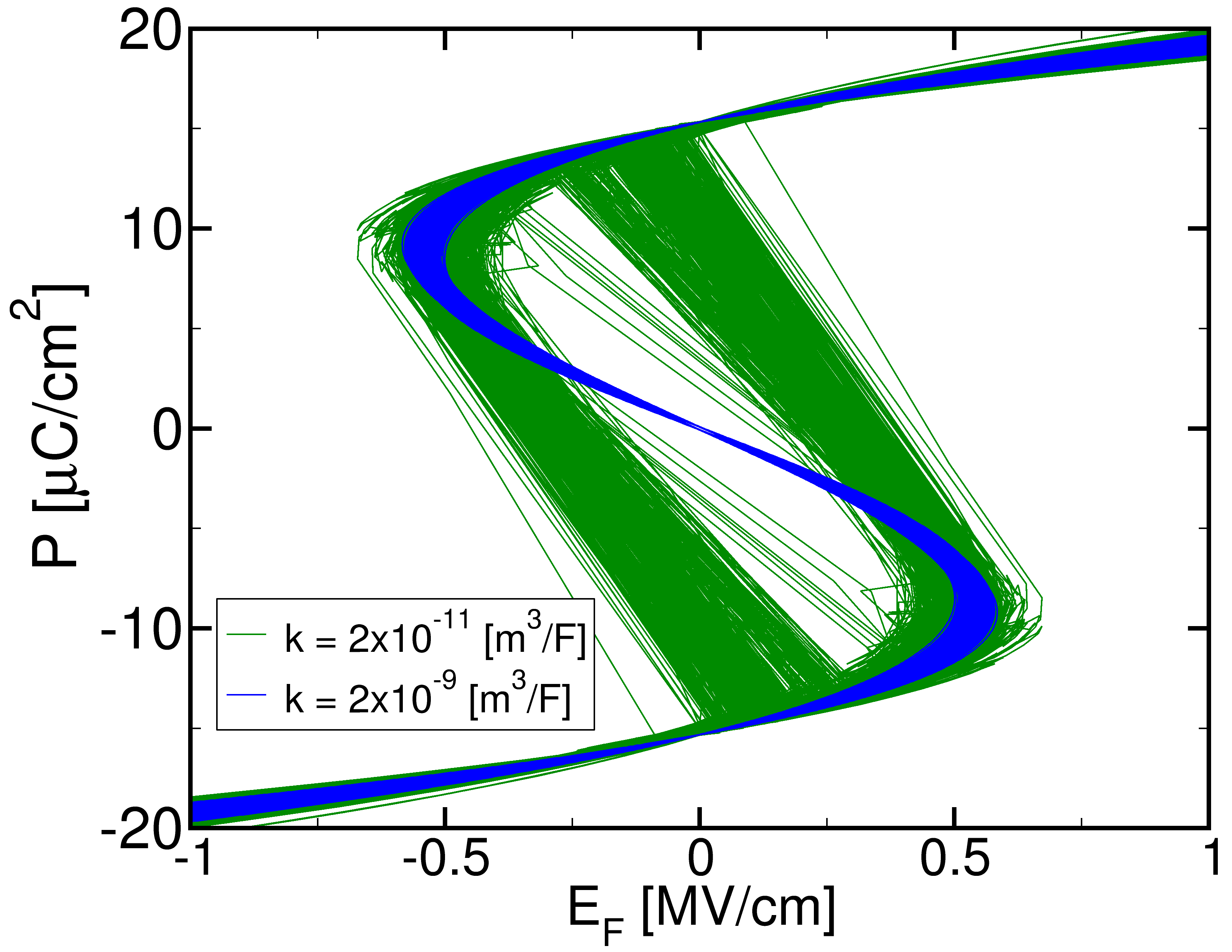
From the standpoint of the multi-domain LGD equations, the NC behaviour corresponds to a strongly correlated domain dynamics as illustrated by the simulations reported in Fig.2 and obtained with the modelling approach discussed in [16, 15]. For a relatively large domain wall coupling constant m3/F, the trajectories for all domains are tightly correlated, whereas for a smaller we see that the switching occurs via a domain nucleation process.
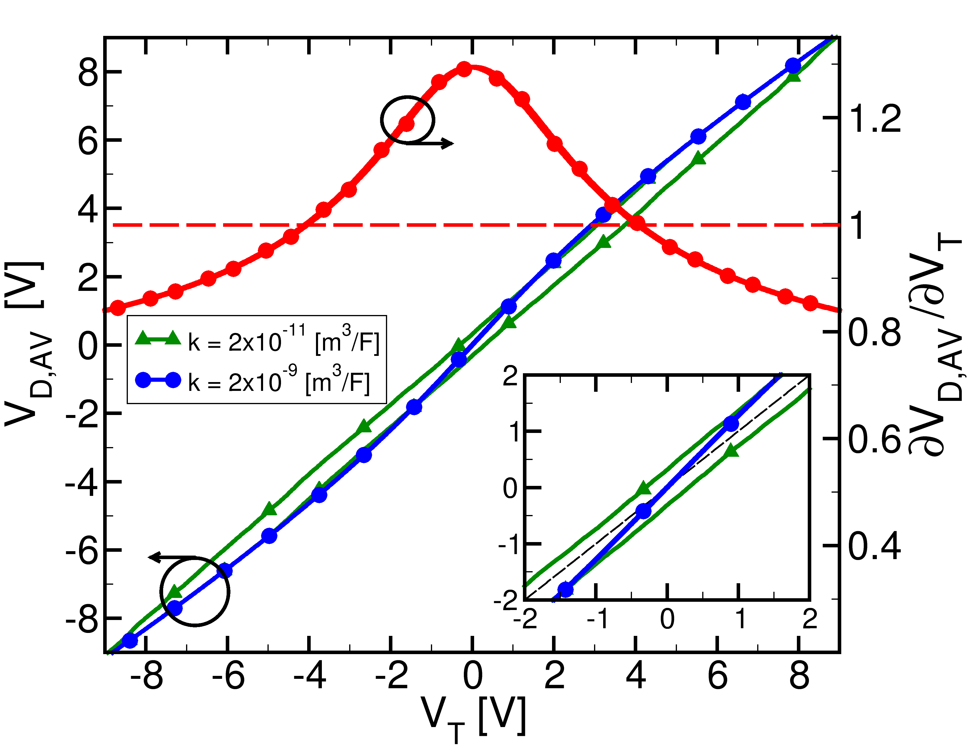
Figure 3 reports the domain averaged voltage drop, , for the values used in Fig.2. The correlated switching process results in a hysteresis free NC behavior and, during the ramp, increase faster than itself, thus leading to a larger than one voltage gain , which is the original idea behind the NC exploitation in nanoscale FETs [1].
The possible advantages of a ferroelectric NC operation have been investigated up to a full-chip level and in a high quality industrial technology [24]. While the benefits of the NC operation on the sub-threshold characteristics of actual transistors seem only modest, design studies for NC transistors are still being actively reported [25, 26, 27].
4 Polarization dependent tunelling in FTJs
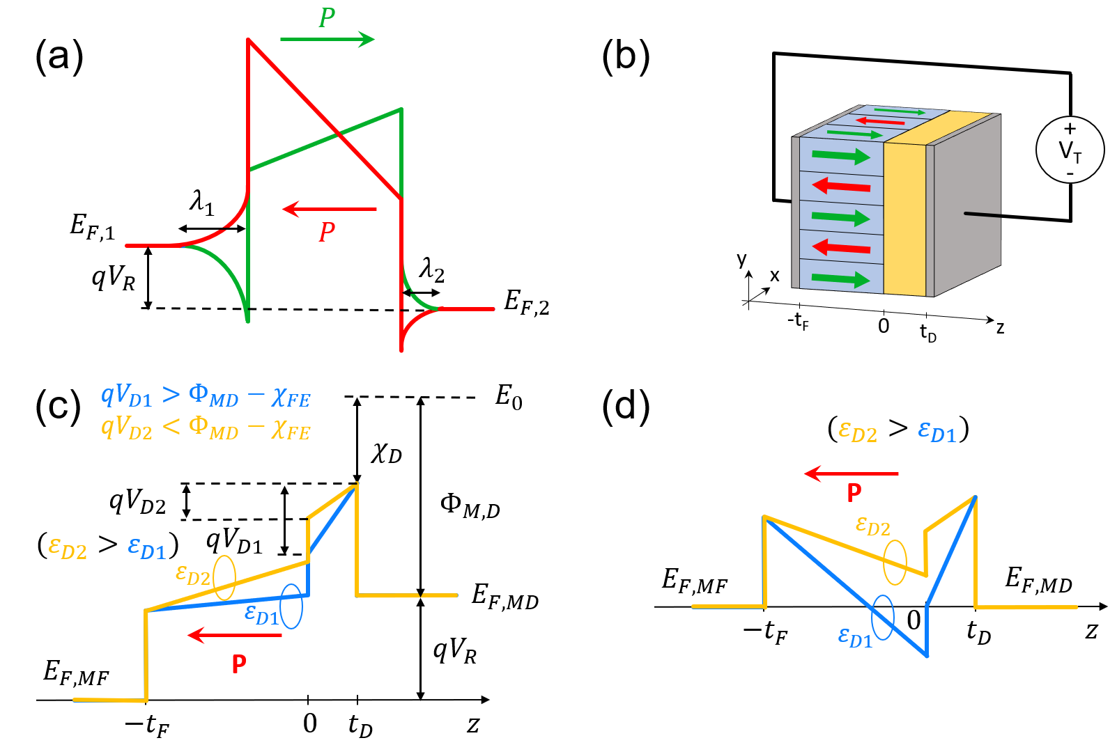
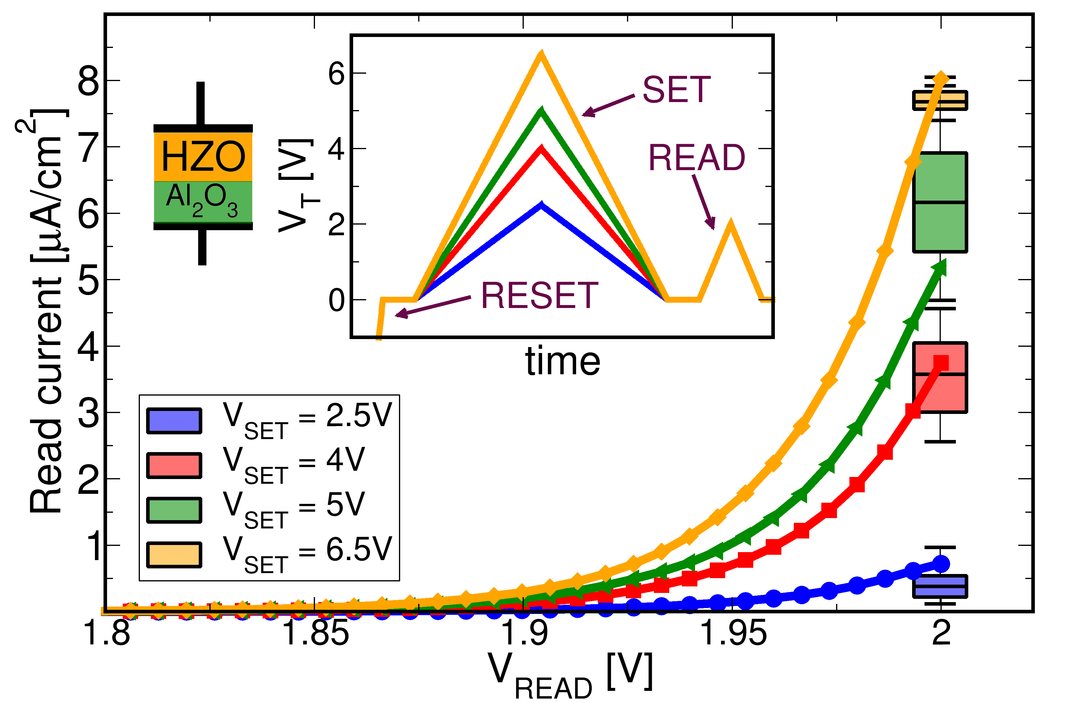
Ferroelectric Tunnelling Junctions (FTJs) are promising candidates as highly energy efficient memristors, in fact the polarization switching is an ultra low energy mechanism to enable the potentiation and depression and, moreover, the readout impedance is very large. The originally proposed FTJ relies on a metal-ferroelectric-metal (MFM) junction [28], whose band diagram is sketched in Fig.4(a). The metal electrodes must have different screening lengths, and , to obtain a polarization dependent tunnelling.
The MFIM architecture sketched in Fig.4(b), instead, separates the switching element and the tunnelling oxide, and an experimental demonstration of a Back-End-Of-Line (BEOL), four level FTJ memristor has been recently reported in [29].
A robust operation of an MFIM based FTJ requires that during reading the oxide voltage drop is large enough to have (see Fig.4(c)), so that tunnelling is limited by the thin dielectric layer. This can be achieved for a small enough which, however, enhances the depolarization field destabilizing the polarization state during retention (see Fig.4(d)). It is evident that device design entails quite delicate tradeoffs that demands a sound modelling support. In this respect, Fig.5 shows the simulated read current characteristics for an HZO/Al2O3 FTJ. A four level operation is observed and the simulated read currents are in fairly good agreement with experiments in [29].
5 Polarization dependent in FeFETs
Ferroelectric FETs (FeFETs) represent an alternative device concept for neuromorphic and in-memory computing systems. Several BEOL-compatible HfO based ferroelectric capacitors [31, 30], as well as ferroelectric memristors have already been demonstrated [34, 33, 32].
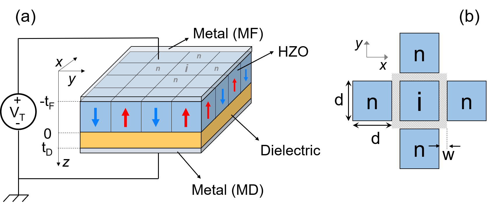
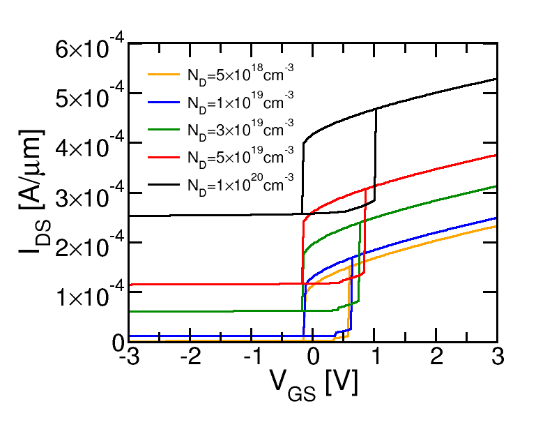
Figure 6 shows a 2D-FeFET with an -type polysilicon active region and, as such, compatible with a BEOL integration. Simulation results are obtained using Sentaurus TCAD and are reported in Fig.7 for very different values of channel doping concentrations. Because the ferroelectric layer is placed between a metal electrode and a semiconductor channel material, the semiconductor depletion can set serious limitations to the ferroelectric switching to a negative polarization (i.e. a polarization pointing to the metal contact, see Fig.6).
In this respect, a high channel doping concentration can avoid the complete depletion of the thin polysilicon layer during the switching to negative polarization. While this is a desirable behavior from a polarization switching perspective, high doping concentrations reduce the conductance modulation induced by the ferroelectric switching, as it is shown in Fig.7. On the other hand doping concentrations lower than about 1019 cm-3 can enlarge the difference in the read current for positive and negative polarization (see Fig.7), however during the switching to negative polarization the polysilicon gets fully depleted and a minority carrier inversion is needed. In this case the physical mechanisms for the supply of minority carriers become crucial.
For an SRH generation of minority carriers we need small carrier lifetimes, in which case the polysilicon channel can help because the defects at the grain boundaries largely enhance the generation rates compared to mono-crystal silicon [35]. An alternative design option may be give by mid-gap Schottky contacts able to supply both electrons and holes, but at the cost of a larger contact resistance.
6 Outlook and conclusions
The ferroelectricity has introduced substantial innovation in the design of electron devices. The support of modelling and simulation is important to unleash the potentials of these materials, particularly in new applications such as hybrid memristive-CMOS neuromorphic processing systems.
Acknowledgements: This work was supported by the European Union through the BeFerroSynaptic project (GA:871737).

References
-
[1]
S. Salahuddin and S. Datta, Nano Letters, vol. 8, n.2, 2008.
-
[2]
A.C. Seabaugh et al., Proc. of IEEE, vol. 98, n. 12, pp.2095-2110, 2010.
-
[3]
A. M. Ionescu and H. Riel, Nature, vol. 479, pp.329-337, 2011.
-
[4]
D. Esseni et al.,
Semicond. Science and Techn., vol. 32, p. 083005, 2017
-
[5]
H. Wang et al., IEEE EDL, vol.39, n.3, 2018
-
[6]
S. Ambrogio et al., Nature, vol.558, pp.60-67, 2018.
-
[7]
E. Chicca et al., Appl. Phys. Lett., vol. 116, p. 120501, 2020.
-
[8]
S. Yu et al., Proc. of IEEE, vol. 106, n. 2, p.260, 2018.
-
[9]
T. S. Böscke et al., 2011 Proceed. of IEDM, pp.24.5.1-24.5.4, 2011.
-
[10]
D. Zhou et al., Acta Materialia, vol. 99, pp. 240-246, 2015.
-
[11]
T. Mikolajick et al., Proceed. of IEDM, pp. 15.5.1-15.5.4, 2019.
-
[12]
S. Slesazeck et al., Nanotechnology, vol. 30, p. 352003, 2019.
-
[13]
M. Hoffmann et al., Nanoscale, vol. 10, pp.891-899, 2018.
-
[14]
H. W. Park et al., Adv. Mater., vol.31, n.1805266, 2019.
-
[15]
T. Rollo et al., Nanoscale, vol. 12, pp.6121-6129, 2020.
-
[16]
T. Rollo et al., Proceed. of IEDM, pp.142-145, 2019.
-
[17]
A. I. Khan et al., Nature Materials Letters, vol.14, pp.182-186, 2015.
-
[18]
S. Song et al., Sci. Rep., vol.6, p. 20825, 2016.
-
[19]
K. S. Li et al., Proceed. of IEDM, vol.6, pp. 22.6.1-22.6.4, 2015.
-
[20]
M. H. Lee et al., Proceed. of IEDM, pp. 12.1.1-12.1.4, 2016.
-
[21]
P. Sharma et al., Symposium on VLSI Tech., pp. T154-T155, 2017.
-
[22]
M. Hoffmann et al., Proceed. of IEDM, vol.565, pp.31.6.1–31.6.4, 2018.
-
[23]
M. Hoffmann et al., Nature, vol.565, pp.464-467, 2019.
-
[24]
Z. Krivokapic et al., Proceed. of IEDM, pp.357-360, 2017.
-
[25]
T. Rollo et al., IEEE EDL, vol.39, n.4, pp.603-606, 2018
-
[26]
T. Rollo et al., Proceed. of IEDM, pp. 213-216, 2018.
-
[27]
S. Esaki et al., IBM Tech. Discl. Bull. 13 ,2161, 1971.
-
[28]
L. Pentapati et al., IEEE TED, VOL. 67, p.365-370, 2020.
-
[29]
B. Max et al., Journal of Electr. Dev. Soc., vol.7, pp.1175-1181, 2019.
-
[30]
T. Francois et al., Proceed. of IEDM, pp. 362-365, 2019.
-
[31]
Y.D. Lin et al., Proceed. of IEDM, pp. 346-349, 2019.
-
[32]
M. Halter et al., ACS Appl. Mater. Int., vol. 12, pp. 17725-17732, 2020.
-
[33]
F. Mo et al., IEEE JEDS, vol. 8, pp. 717-723, 2020.
-
[34]
K. Ni et al., Proceed. of IEDM, pp. 296-299, 2018.
-
[35]
P. K. Hurley et al., App. Phys. Lett., vol.54, pp.1525-1527, 1989.