Further author information: (Send correspondence to Thomas Gascard)
E-mail: thomas.gascard@astro.cf.ac.uk
Design and experimental investigation of a planar metamaterial Silicon based lenslet
Abstract
The next generations of ground-based cosmic microwave background experiments will require polarisation sensitive, multichroic pixels of large focal planes comprising several thousand detectors operating at the photon noise limit. One approach to achieve this goal is to couple light from the telescope to a polarisation sensitive antenna structure connected to a superconducting diplexer network where the desired frequency bands are filtered before being fed to individual ultra-sensitive detectors such as Transition Edge Sensors. Traditionally, arrays constituted of horn antennas, planar phased antennas or anti-reflection coated micro-lenses have been placed in front of planar antenna structures to achieve the gain required to couple efficiently to the telescope optics. In this paper are presented the design concept and a preliminary analysis of the measured performances of a phase-engineered metamaterial flat-lenslet. The flat lens design is inherently matched to free space, avoiding the necessity of an anti-reflection coating layer. It can be fabricated lithographically, making scaling to large format arrays relatively simple. Furthermore, this technology is compatible with the fabrication process required for the production of large-format lumped element kinetic inductance detector arrays which have already demonstrated the required sensitivity along with multiplexing ratios of order 1000 detectors/channel.
keywords:
Antenna, CMB, Metamaterial, Focal plane, Lens, Phase-engineered, Planar1 INTRODUCTION
Observing the polarisation modes present in the Cosmic Microwave Background (CMB) is an essential step for modern cosmology and calls for precision instruments for which novel technologies are actively investigated, particularly focal plane optical coupling and detector technologies. Focal optics influences the angular response, polarisation properties, bandwidth and efficiency of the coupled detectors. Ideally, such system provides a polarisation-symmetric beam response across the full operating bandwidth. The planar metamaterial based air-gap phase-delay lenslet reported here, following up on initial investigations[1] of a variety of lens design approaches, is a step forward towards enabling large detector array optical coupling necessary for future cosmology experiments. Current investigations are conducted on various focal optic solutions. Corrugated horns made of stacked Silicon platelets[2] offer excellent polarisation properties, important control over the beam width and do not need Anti-Reflection Coating (ARC), but they are constrained in bandwidth and can only be either waveguide fed or directly coupled to the detectors. Phased antenna arrays, as is done for SPIDER[3] and BICEP2/Keck arrays[4] are inherently telecentric, limiting the optical coupling between the detectors and telescope optics. Such technology requires multiple ground planes and microstrip crossovers, leading to a challenging fabrication. At last, detectors can be coupled with an antenna and lens system, as has been done for POLARBEAR2[5] and South Pole Telescope (SPT)-3G[6]. This approach allows the antenna to radiate through a dielectric such as Silicon onto which the lens can sit, increasing the gain response proportionally to the index of refraction while allowing for a smaller antenna design, thus providing extra room for detectors, microstrip based filters, and others. However, the hyper-hemispherical lenses require deposition of an ARC layer which reduces the bandwidth, the spherical surface is rough due to fabrication limits, degrading the performances. Assembling lenslets into an array induces stray light issues in the detector wafer[7] if not compensated by an additional resistive layer. The phase engineered planar meta-lenslet reported here provides a valuable workaround, they share the detector plane fabrication process, offering an integrated solution with attractive manufacturing tolerance, good optical performance, low polarisation systematics and an embedded ARC. Such device can further be coupled with any desired feed while maintaining broadband capabilities. The meta-lens Technology Readiness Level (TRL) is at 2, awaiting experimental validation and on-sky demonstration to progress. In this paper will be presented the phase-engineered design principle behind the device along with preliminary measurements of its performances.
2 METAMATERIAL LENSLET DESIGN
Metamaterials enable striking freedom in shaping light at large scales based on individually tunable minute elements while providing a flat and compact architecture with straightforward manufacturability. When applied to the design of a lens, the approach goes beyond solving conventional lens-maker’s equations. The entire structure consist of a three-dimensional array of metal patches arranged in columns, or pixels. Specifically, the lens constitutive elements can be tuned to match any desired feed, including planar antennas, waveguides, etc., as their transversal phase profile is engineered to transform a circular wave to a planar wave, as illustrated in Fig. 1. Each column is carefully designed via a Transmission Line (TL) based code derived from the meta-mesh filter design techniques and each pixel may be considered as an isolated phase shifting waveguide. A precursor lenslet fully embedded in polypropylene[13][14] has previously been realised using this design approach, demonstrating the working principle presented in this section.
The source at focus initially selected for this lenslet was a chocked circular horn operating in the W-band . The beam response is determined via Finite Element Method (FEM) in High Frequency Structure Simulator (HFSS) [8] and is presented in section 3, Fig. 4. The largest Full Width at Half Maximum (FWHM) angle can then be extracted and the equivalent beam waist produced by the horn is deduced as a function of frequency as per the left part of Eq.1[9]. The Rayleigh distance is then deduced using the right part of Eq.1. It effectively defines the maximal admissible variation for the lens focus position from the probe aperture along the optical axis. Additionally, the phase centre of this probe, origin of the gaussian beam, is obtained from HFSS simulation as the peak-to-peak phase difference of the E-field, found at in front of its aperture.
| (1) |
In order to define the lens focal length given its diametre arbitrarily chosen, a first approximation is to consider it as a thin lens truncating the gaussian beam emitted by the probe. As is described in [10], such a truncated beam profile stays gaussian for a truncation ratio and in this interval there is a trade-off between the power loss at the aperture, increasing with , and the peak axial irradiance, decreasing with , with a maximum reached for . With this constraint in mind, the optimal focal length can be determined at a given frequency, here taken at 90GHz, using Eq. 2.
| (2) |
The apex half-angle of the probe gives a Numerical Aperture (NA) for the lenslet at . Knowing the spot size focused by the lens at the probe aperture should be , the related spot-size constant can be found. The latter relation is valid for . This constant is a function of beam truncation only, and can be evaluated based on the FWHM intensity as or on the Full Width at (FWE2) intensity as . In practice while maximum peak axial illumination is reached with the latter expression, the first provides optimal trade-off between illumination and power, giving . is the beam waist at truncation, positioned at the focal length found to be and giving . Accounting for an offset centre of phase position, found at , the optimal distance from the lens to the feed’s aperture is now fully defined. The phase-engineering procedure is driven by the phase response of the source at on the plane where the lens intersects its beam, obtained in HFSS, as presented in Fig. 2. A column of patches at a given position along the lens radius will in fact provide a phase shift derived from a third degree polynomial fit, with coefficients , of the phase shift averaged from the response at azimuths and as per Eq. 3.
| (3) |
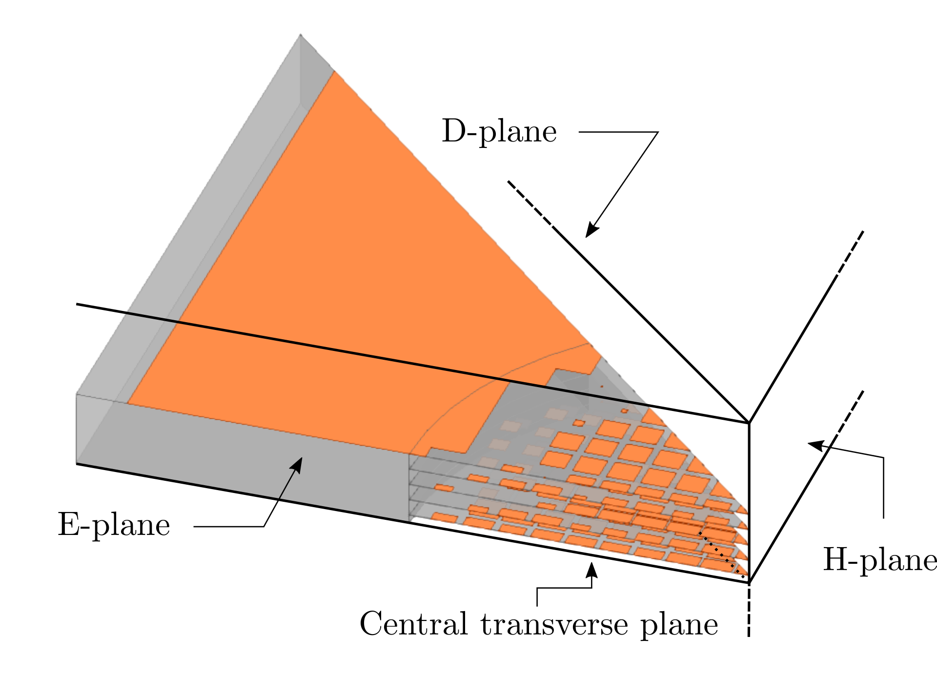
The code at the core of the phase engineering approach finds its roots in meta-mesh filter design[11][12] where a stack of Frequency Selective Surfaces is modelled by a lossless TL of equivalent distributed elements. This is effectively representing the wave propagation in the medium between the adjacent grids, connecting lumped shunt admittances emulating electromagnetic response of the patches. Each constituent of the stack can be seen as a low-pass filter matching a given impedance, here , of resonant angular frequency , normalised frequency , thus a generalised frequency of . It provides a transmitted phase shift , has a characteristic impedance and a transmittance , functions of the FSS geometrical parameters ratio with the half-gap between square patches and is the unit-cell size, as per Eq. 4. The transmittance is desired above 99%, requiring at thus . For the column under investigation, each constituent’s geometry is refined via a Markov Chain Monte Carlo (MCMC) optimisation. To lighten the computing load, E,H,D and central transverse plane symmetries are introduced, bringing the effort down to a half-section of an octant of the lens with elements per columns, where is now necessarily even. To initiate the code, the optimal number of layers is determined by refining the and of the central column, for which the highest phase shift is desired.
| (4) |
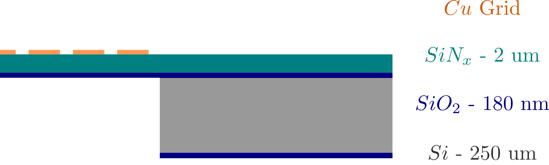
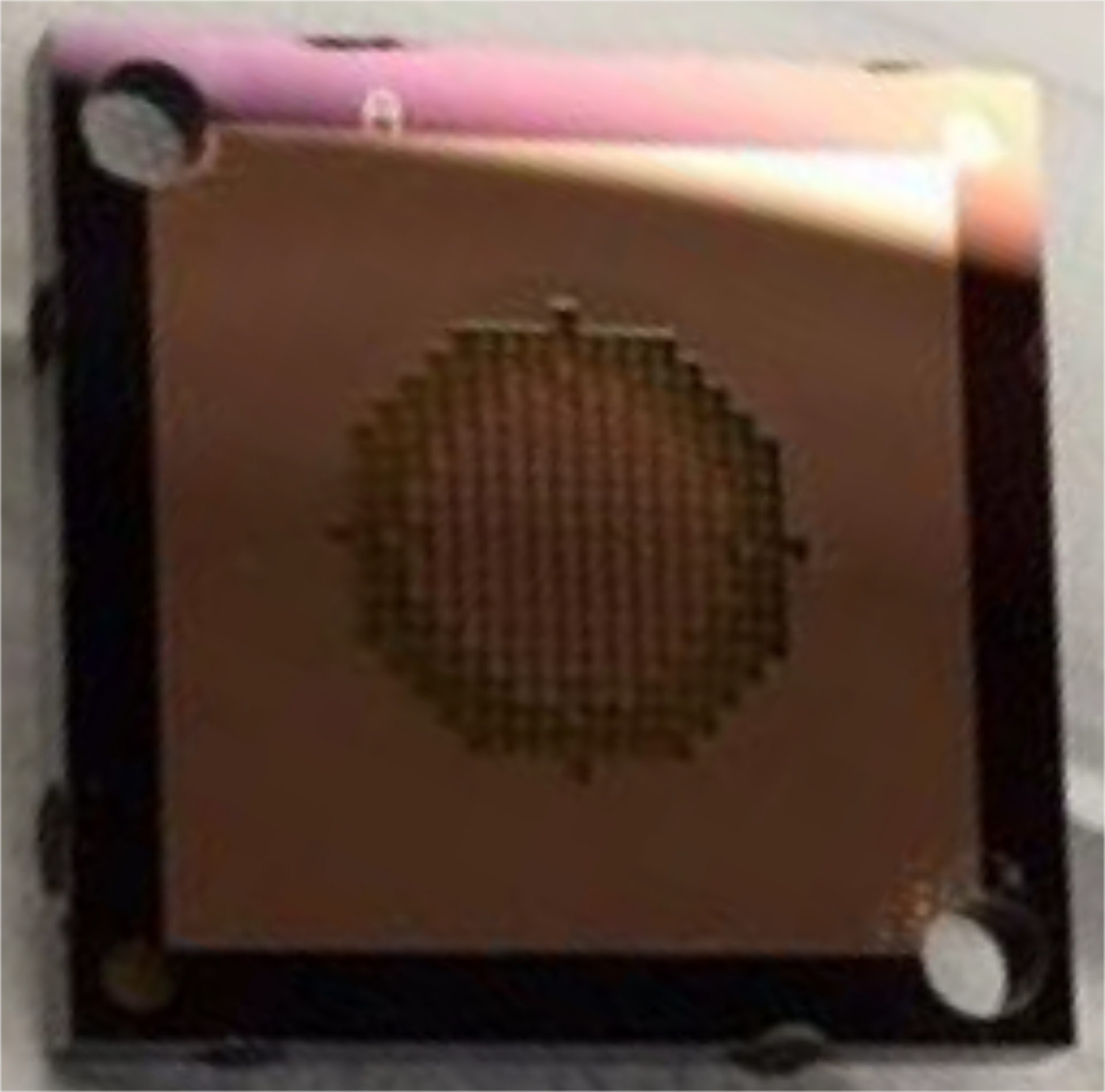
The half-octant is presented in Fig. 3 along with the fabricated lens comporting layers for 40 refined columns. The copper deposition provides a feature thickness at . As such material has a skin depth of at , the grids can be considered as infinitely thin. These FSS are photolithographed on a thin Chemical Vapor Deposition (CVD) silicon nitride substrate sitting on Deep Reactive Ion Etching (DRIE) silicon rims, giving a air-gap between each layer. This lenslet is effectively a demonstrator for the phase-engineering design, it has been compared with the GRadient INdex (GRIN) approach [1]. The next stage will be to generate a structure fully embedded in Silicon, allowing efficient coupling with photolithographed feed such as planar antennas, offering excellent unidirectional radiation in such thick dielectric substrate and flexibility in the underlying microstrip line feeding the detectors.
3 LENSLET PRELIMINARY MEASUREMENTS
Validation of the expected performances of the phase-engineered design approach is an important milestone in the TRL progression of the meta-mesh lens. Performances shown in simulations needs to be demonstrated experimentally to reach the third stage. In this section, the simulated device characteristics are presented alongside preliminary experimental validation.
3.1 Probe characterisation
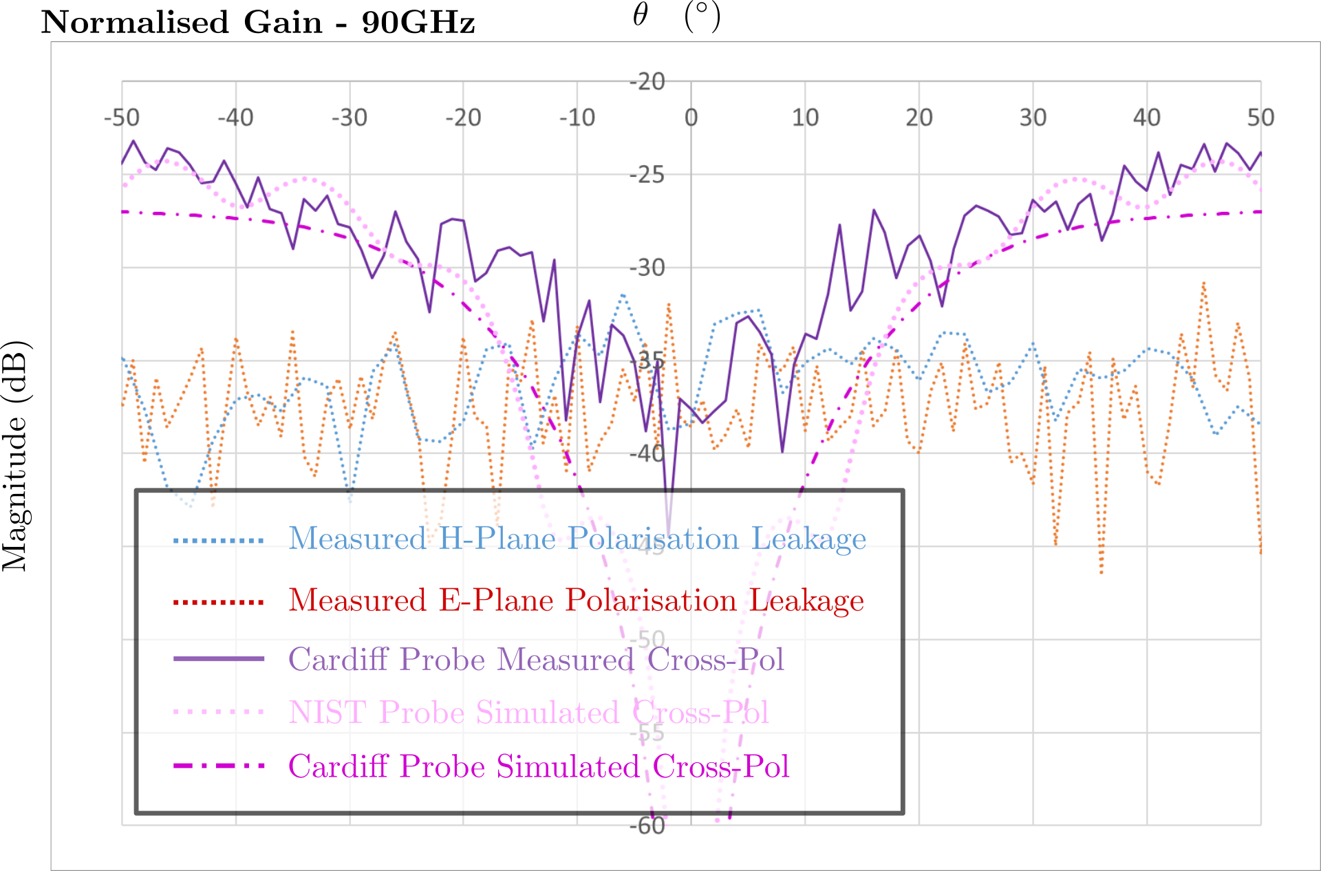
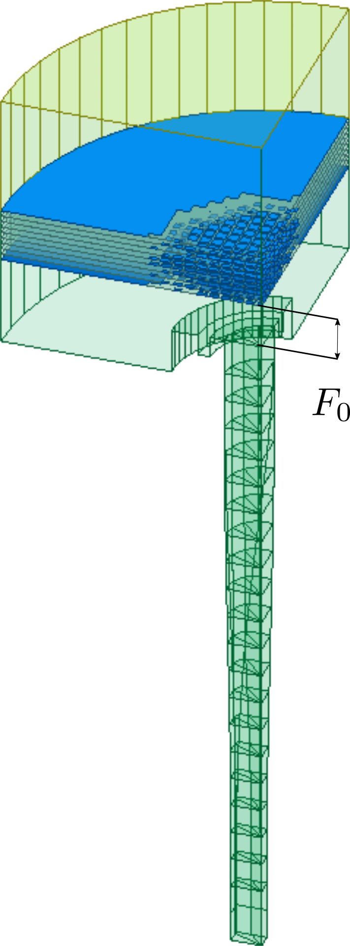
The feeding element coupled to the lenslet is critical, as has been seen in Section 2. Regrettably, the dedicated commercial horn was unavailable in the laboratory. A custom waveguide transition was used instead, transferring light from a WR10 rectangular aperture to a circular aperture of radius , further chocked[15] to obtain a better homogeneity of the beam response and to reduce cross-polarisation. The choke optimal geometry is given for a flange width , choke distance from the waveguide wall , width and depth . The waveguide transition design and simulated beam response are shown in Fig. 4 at the frequency . The patterns can be compared with the aforementioned commercial horn response also present in this figure, showing a similar gaussian beam of waist . Comparison of the measured and simulated responses of the waveguide transition are provided in Fig. 5, showing a cross-polarisation level of at worst. Its phase centre position is at the aperture . Such substitute feed is perfectly suitable to feed the lenslet if positioned at the proper distance found to be at the new focal length derived from Eq. 2. Measured response of this converter is also showed in Fig. 4, showing excellent agreement for the azimuth range , with a gaussian fit matched down to accuracy.
3.2 Pre-analysis via simulations
With confidence in the modelled probe feeding the system, coupling with the lenslet can be conducted. A first model is investigated to validate the focal length by refining the separation between the lenslet and the feed’s aperture. Once the focal length is confirmed, a fine simulation of the response is carried out and serves as the validation baseline for the measurements conducted in the laboratory. The model is illustrated in Fig. 6 and provided an optimal beam response at the expected focal length . The selection is made on the maximum peak gain and FWHM, the best beam homogeneity comparing the E, H and D-plane responses, the highest beam gaussianity, but also on the lowest levels of cross-polarisation and first sidelobe. The gaussianity of the beam is established to the order by operating a regression analysis using least squares to fit an -modded gaussian function to the actual response and estimate the error.
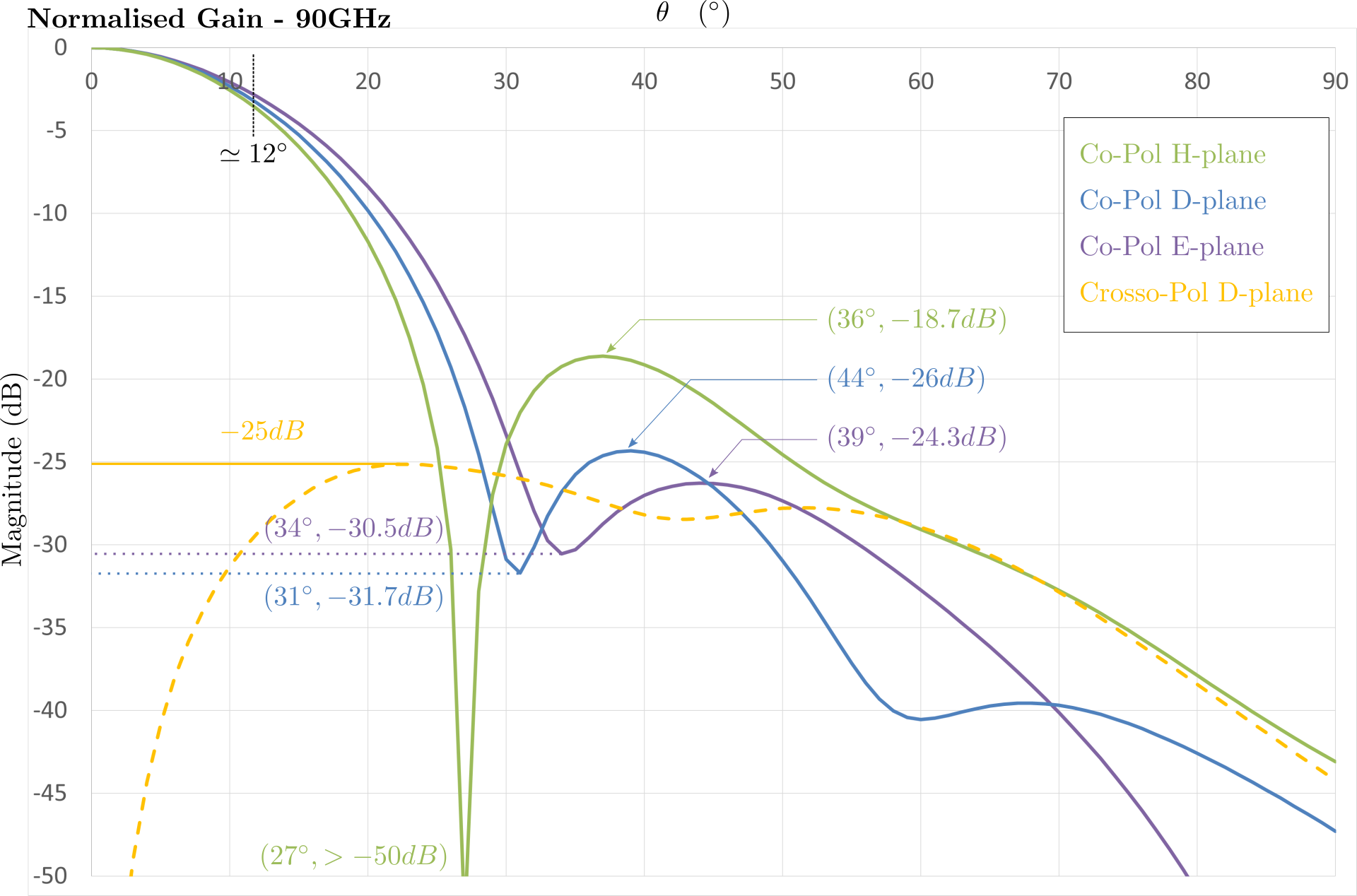
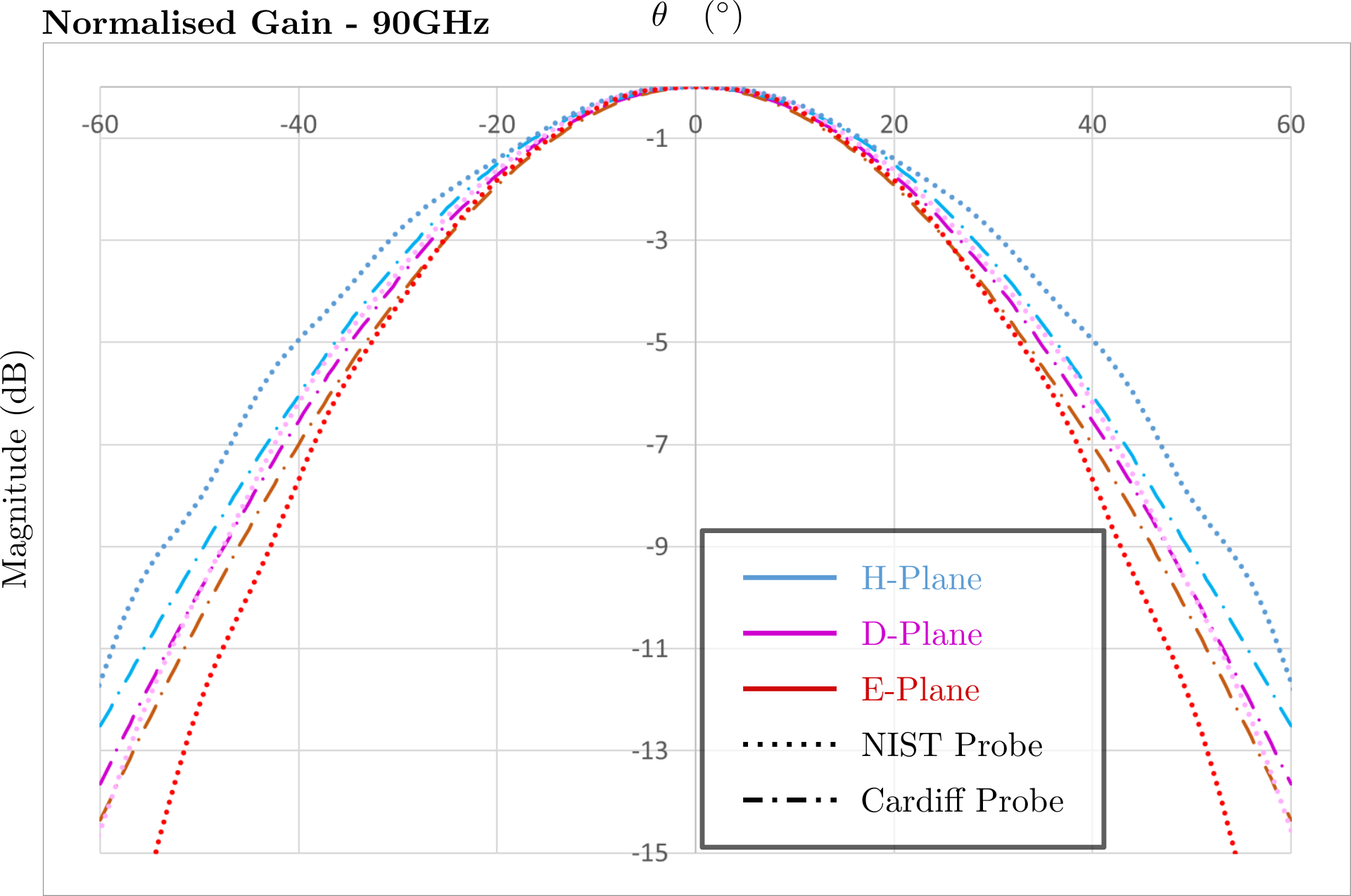
The simulated response is as expected for a lens, with , providing good gaussianity and homogeneity between the different planes down to , with a peak gain at or , first null levels are below and reached around . The FWHM is , first sidelobe levels are equal to or below , and the cross-polarisation level is at worst. This analytical validation of the phase-engineered lenslet design principle can now be compared with measured data.
3.3 Procedure
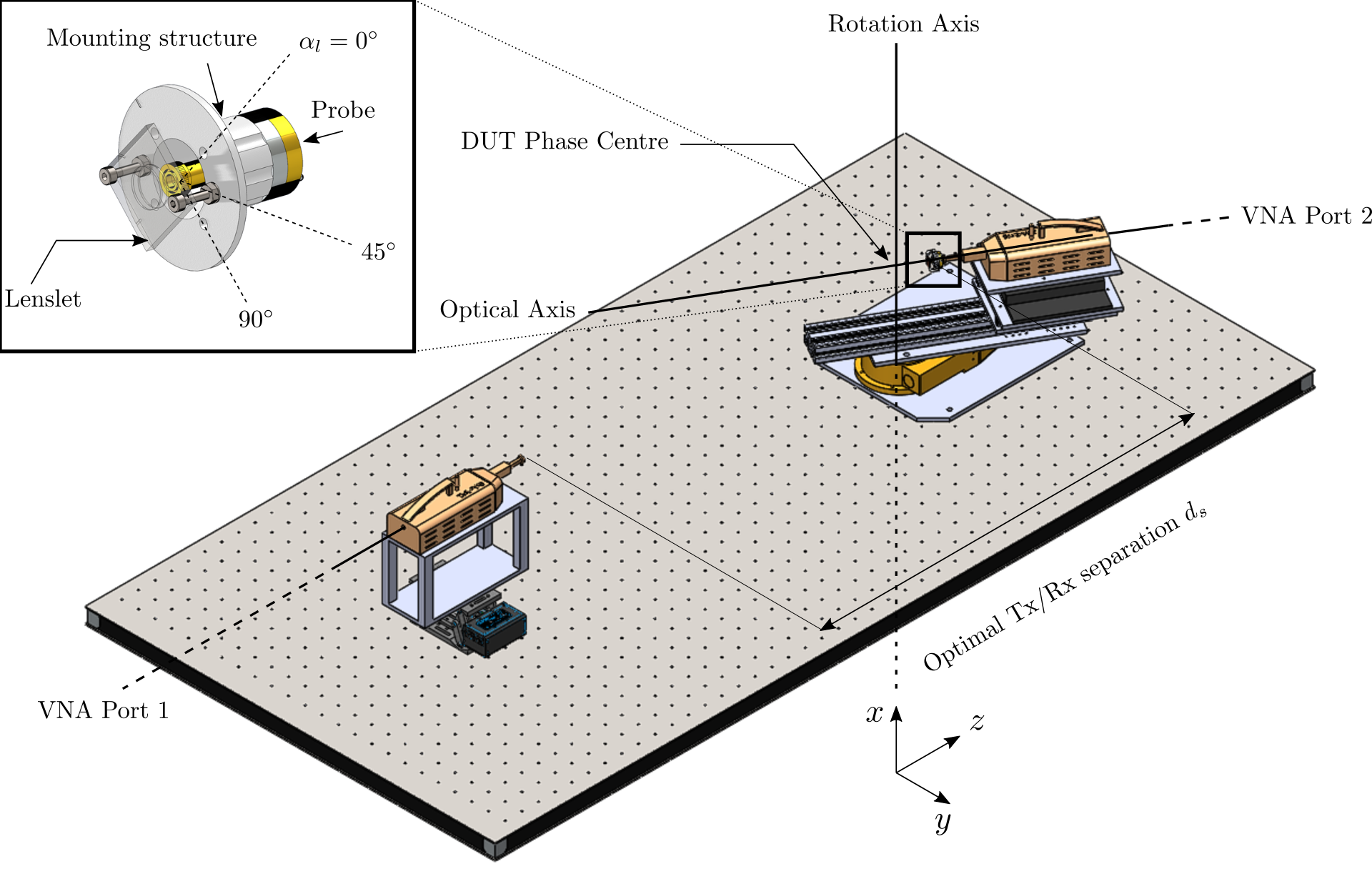
In order to map the co and cross-polarisation beams on the E, H and D-planes while covering the W-band , the experimental setup illustrated in Fig. 7 is designed so that a stationary Transmitter (Tx) feeds a divergent beam to the Device Under Test (DUT). The outgoing plane wave is transmitted to a Receiver (Rx) positioned in the device’s far field. The lenslet and the Tx are assembled together as shown in the insert on Fig. 7 and mounted on a rotary stage, enabling the assembly to rotate through the desired elevation range around the device’s phase centre on the -plane. The Optical Axis (OA) is then defined by the horizontal axis going through the DUT, Tx and Rx phase centres when aligned together. The lenslet can in principle be rotated around the OA at an angle , or . To cover the W-band a set of Rhode & Schwarz (R&S) [16] ZVA Z110 frequency converters are used along with the R&S ZVA67 Vector Network Analyser (VNA). Optimal standing waves attenuation versus dynamic range is achieved at a certain distance between the Rx and Tx probes, here found at . Alignment of the mechanical parts on all three axis is done using a laser leveller and fine positioning of the combined DUT and Tx assembly is conducted so that the DUT phase centre is on the axis of rotation using a micrometric linear stage. Noise reduction is done using Radiation Absorbent Material (RAM) extensively to cover reflective area contributing to the device far field and the feed’s gaussian beam. Measurements are taken via a dedicated software enabling the automated rotation of the DUT and Rx while compiling the transmission from port 1 to port 2 taken from the VNA. The proprietary software provides dataset of 1001 frequency points over the full bandwidth taken back and forth through the elevation interval two times, for the left-hand and right-hand rotations. An averaging over these four passes is done in the post-processing, aiding systematic noise reduction to the VNA embedded averaging capability, set at 16, which gives a total of 64 averages on the data.
3.4 Measurement results analysis
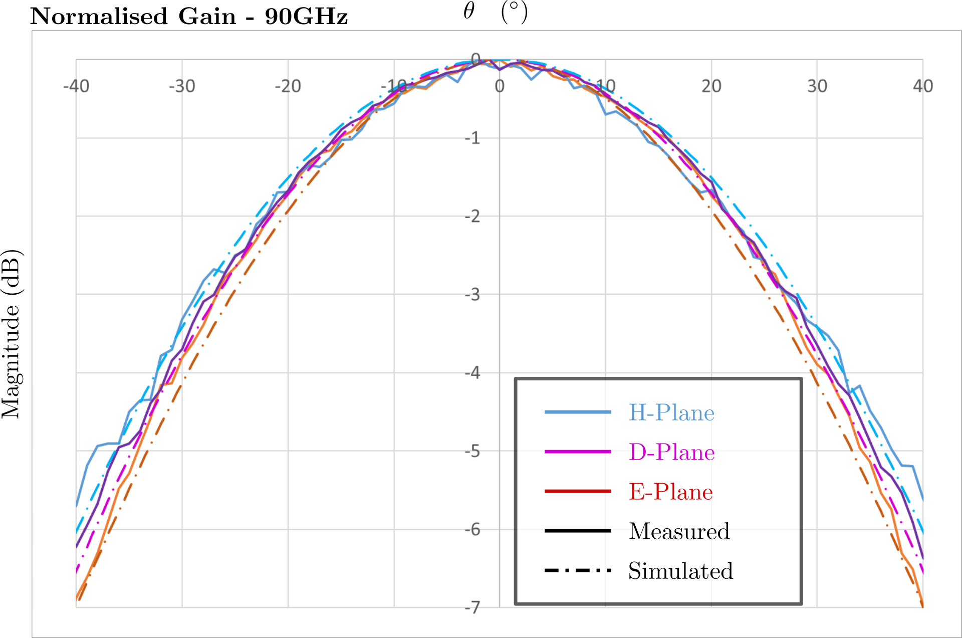
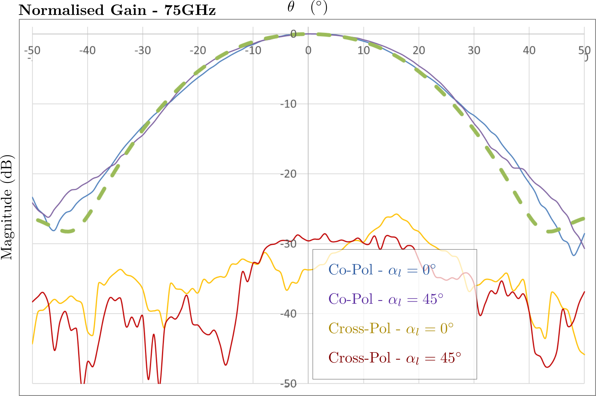
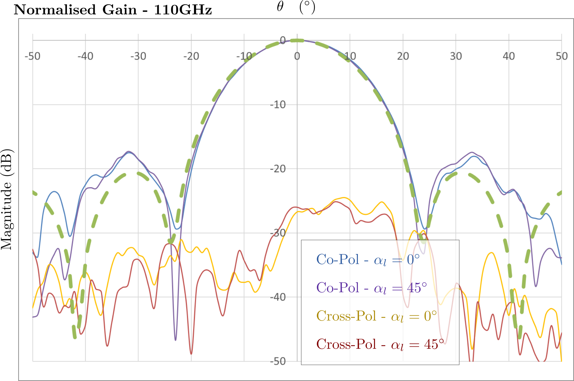
The mounting structure adopted for this experiment limited the distance between the lenslet and the feed at , still within range of focus . The measured beams at , and are presented in Fig. 8(a), 8(b) and 8(c) respectively, where simulations have been carried out to match the new distance . For each frequency, the polarisation leakage and the co-polarisation in the H-plane have been measured with the lens orientated at and . Three main characteristics can be analysed from these data, the main lobe response, the first side-lobe and the polarisation leakage level.
-
•
Main lobe The simulated and measured main lobes matches well over the entire bandwidth. Looking at the beam, the first null level is reaching at FWE2 equal to , FWHM is , giving a beam width of . For the two positions of the device, excellent beam homogeneity and gaussianity is observed throughout the full bandwidth.
-
•
First Side-lobe The side-lobe peak levels and sizes are in accordance with the simulated response, although there is additional noise contribution from the surrounding at high angle of incidence at which the RAM performances decreases.
-
•
Polarisation Leakage The H-plane normalised polarisation leakage levels are consistently below over the full bandwidth and for both position of the device, demonstrating expected performances. The peak value for non-normalised data is close to and drops down to the noise floor of the experimental setup.
Whilst these preliminary results are partially validating the lenslet performances, they are incomplete. Co and cross-polarisation measurements in the E and D planes are awaited and polarisation leakage is still to be checked. Despite an experimental setup offering all capabilities to realise such campaign, the mounting strategy presented notable mechanical risks for the lenslet integrity, it also contributed to the far field response at low frequencies and did not enable easy rotation of the lenslet around the OA. The choice was made to move onto a different mounting strategy for which a separate measurement campaign will be conducted in the near future.
4 CONCLUSION
A comprehensive description of the phase-engineered design procedure of a flat meta-lenslet has been covered, and the resulting performances have been modelled and partially demonstrated experimentally. The lenslet offers a gaussian and homogeneous beam response in the H-plane with sufficient first null level of , an absolute peak gain at , or , at , and polarisation leakage level below . A complete characterisation of the device will be conducted in the laboratory in the near future, addressing the discrepancy between modelled and measured response at lower frequencies. A simulated coupling with a planar sinuous antenna is under investigation and will allow a cryogenic testing of both an Ortho-Mode Transducer (OMT) coupled and antenna coupled lenslet to validate proper detection response opening the path for large array fabrication. While this air-gap lenslet serves as a demonstrator for the design procedure, a fully silicon embedded version is under investigation and should offer a simple solution to Lumped Element Kinetic Inductance Detectors coupling with fabrication processes reduced to minimal effort.
Acknowledgements.
This work was supported in part by the Science and Technology Facilities Council [grant number ST/S00033X/1] and in part by NASA under grant/cooperative agreement number NNX17AE85G.References
- [1] Pisano, G., Austermann, J., Beall, J., Halverson, N., Hubmayr, J., Jaehnig, G., McKenney, C. M., Raymond, B., and Suzuki, A., “Development of Flat Silicon-Based Mesh Lens Arrays for Millimeter and Sub-millimeter Wave Astronomy,” J Low Temp Phys 199 (Jan. 2020).
- [2] Simon, S. M., Austermann, J., Beall, J. A., Choi, S. K., Coughlin, K. P., Duff, S. M., Gallardo, P. A., Henderson, S. W., Hills, F. B., Ho, S.-P. P., Hubmayr, J., Josaitis, A., Koopman, B. J., McMahon, J. J., Nati, F., Newburgh, L., Niemack, M. D., Salatino, M., Schillaci, A., Schmitt, B. L., Staggs, S. T., Vavagiakis, E. M., Ward, J., and Wollack, E. J., “The design and characterization of wideband spline-profiled feedhorns for Advanced ACTPol,” 991416 (July 2016).
- [3] Gualtieri, R., Filippini, J. P., Ade, P. A. R., Amiri, M., Benton, S. J., Bergman, A. S., Bihary, R., Bock, J. J., Bond, J. R., Bryan, S. A., Chiang, H. C., Contaldi, C. R., Doré, O., Duivenvoorden, A. J., Eriksen, H. K., Farhang, M., Fissel, L. M., Fraisse, A. A., Freese, K., Galloway, M., Gambrel, A. E., Gandilo, N. N., Ganga, K., Gramillano, R. V., Gudmundsson, J. E., Halpern, M., Hartley, J., Hasselfield, M., Hilton, G., Holmes, W., Hristov, V. V., Huang, Z., Irwin, K. D., Jones, W. C., Kuo, C. L., Kermish, Z. D., Li, S., Mason, P. V., Megerian, K., Moncelsi, L., Morford, T. A., Nagy, J. M., Netterfield, C. B., Nolta, M., Osherson, B., Padilla, I. L., Racine, B., Rahlin, A. S., Reintsema, C., Ruhl, J. E., Runyan, M. C., Ruud, T. M., Shariff, J. A., Soler, J. D., Song, X., Trangsrud, A., Tucker, C., Tucker, R. S., Turner, A. D., List, J. F. v. d., Weber, A. C., Wehus, I. K., Wiebe, D. V., and Young, E. Y., “SPIDER: CMB Polarimetry from the Edge of Space,” J Low Temp Phys 193, 1112–1121 (Dec. 2018).
- [4] Array, K., Collaborations, B., Ade, P. A. R., Ahmed, Z., Aikin, R. W., Barkats, D., Benton, S. J., Bischoff, C. A., Bock, J. J., Bowens-Rubin, R., Brevik, J. A., Buder, I., Bullock, E., Buza, V., Connors, J., Cornelison, J., Crill, B. P., Crumrine, M., Dierickx, M., Duband, L., Filippini, J. P., Fliescher, S., Grayson, J., Hall, G., Halpern, M., Harrison, S., Hildebrandt, S. R., Hilton, G. C., Hui, H., Irwin, K. D., Kang, J., Karkare, K. S., Karpel, E., Kaufman, J. P., Keating, B. G., Kefeli, S., Kernasovskiy, S. A., Kovac, J. M., Kuo, C. L., Larsen, N. A., Lau, K., Leitch, E. M., Lueker, M., Megerian, K. G., Moncelsi, L., Namikawa, T., Netterfield, C. B., Nguyen, H. T., O’Brient, R., Ogburn IV, R. W., Palladino, S., Pryke, C., Racine, B., Richter, S., Schillaci, A., Schwarz, R., Sheehy, C. D., Soliman, A., Germaine, T. S., Staniszewski, Z. K., Steinbach, B., Sudiwala, R. V., Teply, G. P., Thompson, K. L., Tolan, J. E., Tucker, C., Turner, A. D., Umilta, C., Vieregg, A. G., Wandui, A., Weber, A. C., Wiebe, D. V., Willmert, J., Wong, C. L., Wu, W. L. K., Yang, H., Yoon, K. W., and Zhang, C., “BICEP2 / Keck Array XI: Beam Characterization and Temperature-to-Polarization Leakage in the BK15 Dataset,” ApJ 884, 114 (Oct. 2019). arXiv: 1904.01640.
- [5] Inoue, Y., Ade, P., Akiba, Y., Aleman, C., Arnold, K., Baccigalupi, C., Barch, B., Barron, D., Bender, A., Boettger, D., Borrill, J., Chapman, S., Chinone, Y., Cukierman, A., de Haan, T., Dobbs, M. A., Ducout, A., Dünner, R., Elleflot, T., Errard, J., Fabbian, G., Feeney, S., Feng, C., Fuller, G., Gilbert, A. J., Goeckner-Wald, N., Groh, J., Hall, G., Halverson, N., Hamada, T., Hasegawa, M., Hattori, K., Hazumi, M., Hill, C., Holzapfel, W. L., Hori, Y., Howe, L., Irie, F., Jaehnig, G., Jaffe, A., Jeong, O., Katayama, N., Kaufman, J. P., Kazemzadeh, K., Keating, B. G., Kermish, Z., Keskitalo, R., Kisner, T. S., Kusaka, A., Le Jeune, M., Lee, A. T., Leon, D., Linder, E. V., Lowry, L., Matsuda, F., Matsumura, T., Miller, N., Mizukami, K., Montgomery, J., Navaroli, M., Nishino, H., Paar, H., Peloton, J., Poletti, D., Puglisi, G., Raum, C. R., Rebeiz, G. M., Reichardt, C. L., Richards, P. L., Ross, C., Rotermund, K. M., Segawa, Y., Sherwin, B. D., Shirley, I., Siritanasak, P., Stebor, N., Stompor, R., Suzuki, J., Suzuki, A., Tajima, O., Takada, S., Takatori, S., Teply, G. P., Tikhomirov, A., Tomaru, T., Whitehorn, N., Zahn, A., and Zahn, O., “POLARBEAR-2: an instrument for CMB polarization measurements,” 99141I (Aug. 2016).
- [6] Carter, F. W., Cecil, T. W., Chang, C. L., Cho, H.-M., Cliche, J.-F., Crawford, T. M., Cukierman, A., Denison, E. V., de Haan, T., Ding, J., Dobbs, M. A., Dutcher, D., Everett, W., Foster, A., Groh, J. C., Gilbert, A., Halverson, N. W., Harke-Hosemann, A. H., Harrington, N. L., Henning, J. W., Hilton, G. C., Holder, G. P., Holzapfel, W. L., Huang, N., Irwin, K. D., Jeong, O. B., Jonas, M., Khaire, T. S., Knox, L., Kofman, A. M., Korman, M., Kubik, D. L., Kuhlmann, S., Kuo, C.-L., Lee, A. T., Leitch, E. M., Lowitz, A. E., Meyer, S. S., Michalik, D., Montgomery, J., Nadolski, A., Natoli, T., Ngyuen, H., Noble, G. I., Novosad, V., Padin, S., Pan, Z., Pearson, J., Posada, C. M., Rahlin, A., Reichardt, C. L., Ruhl, J. E., Sayre, J. T., Shirokoff, E., Smecher, G., Sobrin, J. A., Stark, A. A., Story, K. T., Suzuki, A., Thompson, K. L., Tucker, C., Vale, L. R., Vanderlinde, K., Vieira, J., Wang, G., Whitehorn, N., Yefremenko, V., Yoon, K. W., Young, M., Bender, A. N., Ade, P. A. R., Ahmed, Z., Anderson, A. J., Avva, J. S., Barry, P. S., Thakur, R. B., Benson, B. A., Bleem, L. S., Byrum, K., Carlstrom, J. E., Aylor, K., Bocquet, S., Dodelson, S., Gallicchio, J., Guns, S., Quan, W., Raghunathan, S., Wu, W. L., and Jones, A., “Year two instrument status of the SPT-3G cosmic microwave background receiver,” in [Millimeter, Submillimeter, and Far-Infrared Detectors and Instrumentation for Astronomy IX ], Zmuidzinas, J. and Gao, J.-R., eds., 2, SPIE, Austin, United States (Aug. 2018).
- [7] Yates, S. J. C., Baryshev, A. M., Yurduseven, O., Bueno, J., Davis, K. K., Ferrari, L., Jellema, W., Llombart, N., Murugesan, V., Thoen, D. J., and Baselmans, J. J. A., “Surface Wave Control for Large Arrays of Microwave Kinetic Inductance Detectors,” IEEE Transactions on Terahertz Science and Technology 7, 789–799 (Nov. 2017).
- [8] “ANSYS HFSS: High Frequency Electromagnetic Field Simulation Software.” Library Catalog: www.ansys.com.
- [9] Goldsmith, P. F., [Quasioptical systems: Gaussian beam quasioptical propagation and applications ], IEEE Press/Chapman & Hall Publishers series on microwave technology and RF, IEEE Press, Piscataway, NJ (1998).
- [10] Urey, H., “Spot size, depth-of-focus, and diffraction ring intensity formulas for truncated Gaussian beams,” Appl. Opt. 43, 620 (Jan. 2004).
- [11] Ulrich, R., “Far-infrared properties of metallic mesh and its complementary structure,” Infrared Physics 7, 37–55 (Mar. 1967).
- [12] Marcuvitz, N., [Waveguide handbook ], no. 21 in IEE electromagnetic waves series, P. Peregrinus on behalf of the Institution of Electrical Engineers, London, UK (1986).
- [13] Pisano, G., Ng, M. W., Ozturk, F., Maffei, B., and Haynes, V., “Dielectrically embedded flat mesh lens for millimeter waves applications,” Appl. Opt., AO 52, 2218–2225 (Apr. 2013). Publisher: Optical Society of America.
- [14] Pisano, G., Maffei, B., Robinson, M., Deo, P., van der Vorst, M., Trappe, N., and Tucker, C., “Planar mesh-lens arrays for millimeter and sub-mm wave focal planes,” in [2016 41st International Conference on Infrared, Millimeter, and Terahertz waves (IRMMW-THz) ], 1–2, IEEE, Copenhagen, Denmark (Sept. 2016).
- [15] James, G., “Radiation properties of 90° conical horns,” Electron. Lett. 13(10), 293 (1977).
- [16] International, R. . S., “AccueilGroup Home (Accueil Groupe).” Library Catalog: www.rohde-schwarz.com.