Topological charge density wave in monolayer NbSe2
I abstract
Despite the progress made in successful prediction of many classes of weakly-correlated topological materials, it is not clear how a topological order can emerge from interacting orders and whether or not a charge ordered topological state can exist in a two-dimensional (2D) material. Here, through first-principles modeling and analysis, we identify a 22 charge density wave (CDW) phase in monolayer -NbSe2 that harbors coexisting quantum spin Hall (QSH) insulator, topological crystalline insulator (TCI) and topological nodal line (TNL) semimetal states. The topology in monolayer NbSe2 is driven by the formation of the CDW and the associated symmetry-breaking periodic lattice distortions and not via a pre-existing topology. Our finding of an emergent triple-topological state in monolayer -NbSe2 will offer novel possibilities for exploring connections between different topologies and a unique materials platform for controllable CDW-induced topological states for potential applications in quantum electronics and spintronics and Majorana-based quantum computing.
II Introduction
A new frontier in condensed matter physics concerns the study of emergent topological phases in correlated materials [1, 2]. Recent proposals, which have focused on realizing a topological charge ordered (TCO) state in materials [3, 4, 5, 6] start by assuming a pre-existing topological order before introducing the charge density wave (CDW) transition. It remains unclear how a topological state could emerge driven by the spontaneous symmetry breaking (SSB) involved in the formation of the CDW itself. Here, our first-principles modeling and analysis shows that a 2×2 CDW phase of a -NbSe2 monolayer film can support a complex topological phase with three co-existing topological states even though a pristine -NbSe2 film has a trivial band topology.
Since the discovery of the quantum spin Hall (QSH) insulator [7, 8, 9], or 2D topological insulator (TI), a variety of topological insulators and semimetals have been proposed in 2D materials such as topological crystalline insulators (TCI) [10, 11] and topological nodal line (TNL) semimetals [12, 13]. Both QSH insulators and TCI are novel quantum materials with insulating bulk states but conducting edge states that are topologically protected either by the time reversal symmetry (TRS) or the crystalline symmetries. It is also possible that the QSH and TCI can coexist in a 2D material preserving both time-reversal and mirror symmetries as, for example, in monolayer Na3Bi [14]. The QSH state with its associated quantized Hall conductance without an external magnetic field was first observed in HgTe/CdTe quantum wells [15, 16]. It has also been predicted [17] and observed experimentally [18, 19] in monolayer transition metal dichalcogenide (TMD) film of WTe2.
TMDs display a dazzling variety of correlated phases, including CDW [20, 21], superconductivity and magnetic orders [22]. In recent years, TMDs have become available as monolayers [23], which are extremely elastic, and can withstand large in-plane strains () [24] and provide an ideal playground for designing topological phases [18, 19, 25] and the manipulation of many-body ground states [26, 27, 28, 29]. In particular, bulk -NbSe2 is one of the most extensively studied TMDs that exhibits both superconductivity ( 7.2 K) [30] and a triangular (3Q) incommensurate CDW with period in real space ( 33 K) [31]. -NbSe2 has strongly layer-dependent properties [32], with monolayer -NbSe2 (also referred as the structure [17]) hosting enhanced 3 period triangular (3Q) CDW order ( K) [33, 34] and weaker superconductivity ( K) [35, 36] which may have an exotic Ising pairing [37, 38].
Scanning tunneling microscopy (STM) experiments find two unexpected CDW phases in monolayer -NbSe2 with applied in-plane biaxial tensile strain: one phase has a triangular (3Q) order with period 2 while the other is a unidirectional stripe (1Q) order with period 4 [39]. A similar unidirectional stripe phase with period has been observed in bulk -NbSe2 [40], but there is no report of a bulk triangular (3Q) order with period 2. Experimentally, the heavily electron-doped monolayer NbSe2 also hosts a 22 CDW order [41]. Ab initio calculations have established the modulated crystal structure of the triangular 3 [42, 43, 44] and stripe 4 [45] CDW phases of monolayer -NbSe2, but the crystal structure of the 22 CDW is not known. Due to the wide application of NbSe2 [46, 23] and the important role of substrate strain in monolayer materials, it is crucial to understand the structural ground state and electronic properties of this phase.
In this article, we discuss ab initio calculations within the density functional theory (DFT) framework to establish the structure of the 22 triangular CDW in monolayer -NbSe2. We show that, by applying an in-plane biaxial tensile strain, the soft phonon mode of the unmodulated structure shifts from momentum 2/3 M to M, which implies that the instability leads to a structural reconstruction related to a triangular period 2 charge order. We find two stable 22 CDW phases with slightly different energies, which are in the pattern of a breathing mode. Above a certain in-plane biaxial strain, the 22 phase becomes the ground state. Finally, we unveil the emergence of non-trivial time-reversal protected and mirror-protected classes of topologies in the CDW phase, and show that the CDW phase of monolayer -NbSe2 hosts three co-existing topological states.
III Strain-induced instabilities
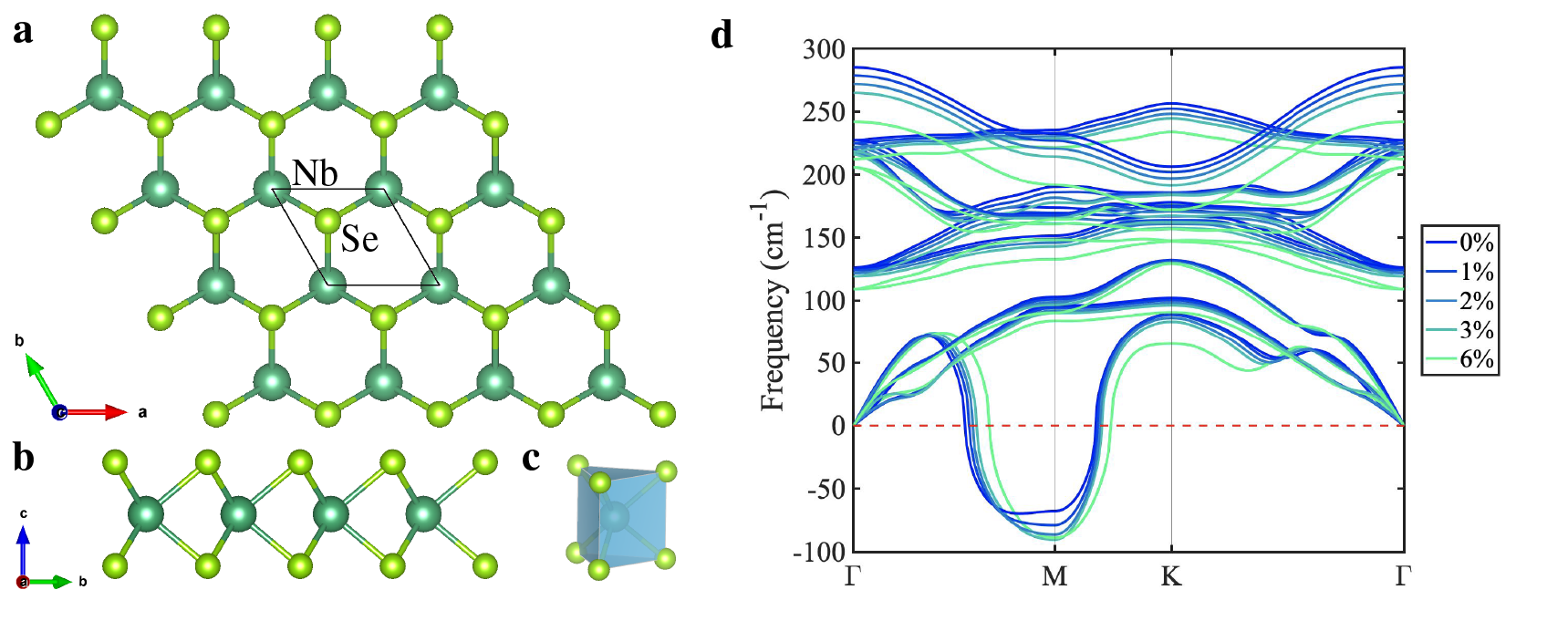
While bulk -NbSe2 is a van der Waals material with centrosymmetric space group (No. 194) containing inversion symmetry, the monolayer -NbSe2 has a non-centrosymmetric (No. 187) space group with an additional out-of-plane mirror symmetry but no inversion symmetry. Fig. 1a shows the top view of the hexagonal structure of monolayer NbSe2, and the Nb layer, which acts as a mirror plane for the , is sandwiched between two Se layers as shown in Fig. 1b. Each Nb atom sits inside a trigonal prismatic cell formed by six nearest-neighbor Se atoms as shown in Fig. 1c. Our calculations show that Nb atoms form a perfect hexagonal close-packed structure, with the shortest Nb-Nb separation = 3.485 Å.
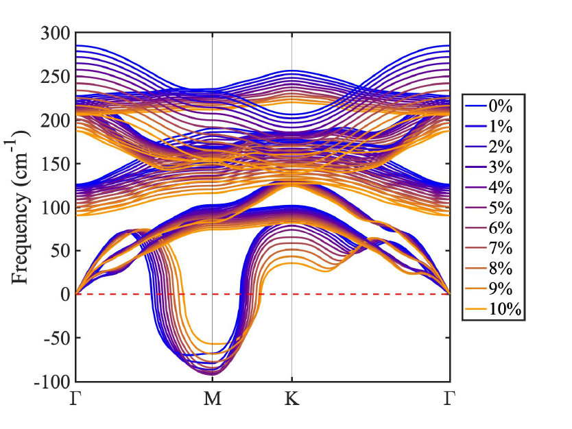
The normal unmodulated phase of monolayer -NbSe2 is found to be unstable below the CDW critical temperature [33, 34] and it exhibits a prominent soft phonon mode around 2/3 M in our calculations, indicating a strong structural instability to CDW formation with a 33 supercell, consistent with experiment [33, 34]. As shown in Fig. 1d and SM S.1., with increasing in-plane biaxial tensile strains, the soft phonon modes shift from 2/3 M to M which implies a structural instability with 22 CDW modulations. [47, 21] This dependence of the soft phonon mode on the applied strain indicates a strain-induced structural phase transition from 33 to 22 CDW phase. Furthermore, the 33 phase competes strongly with the 22 phase when the strain is around 0%-1% due to the relative flatness of the soft phonon mode between 2/3 M and M point. The broad range of -vectors which simultaneously soften is consistent with a phonon-entropy dominated transition [48]. We emphasize that while the strain applied in DFT calculations is not directly comparable to the strain applied in experiment (0.15%), the DFT calculation can still capture the tendency of structural reconstruction by calculating the ground state energy of each phase.
IV 22 CDW breathing mode
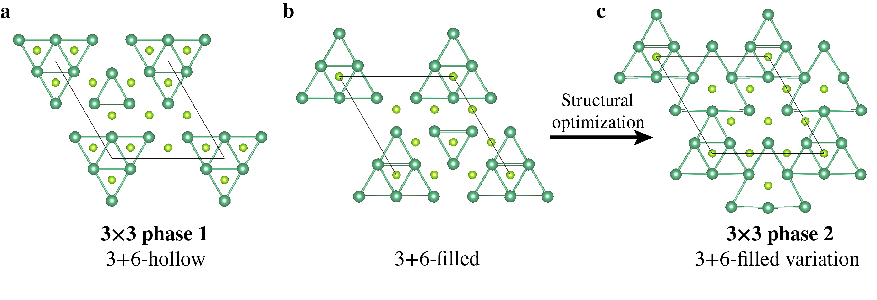
The crystal structure of monolayer -NbSe2 in the CDW state was obtained with multiple structural optimizations with a 22 supercell under different in-plane biaxial tensile strain varying from 0% to 10%. Before each optimization, small in-plane displacements preserving the symmetry were added to Nb atoms on the edge and at the center of the supercell (the triangular Nb trimer), leaving the Nb atoms at the corner of the supercell unchanged. Depending on the direction of the initial displacements, two different phases of CDW modulation emerge after all the atom positions are relaxed in the 22 supercell. With the extended 22 supercell as new unit cell, these two 22 CDW modulated structures have the same space group (No. 187) as the unmodulated structure in the 11 unit cell which reflects the nature of SSB in translational symmetry. The first Brillouin zone of the 22 supercell is accordingly folded from the 11 as shown in Fig. 2e. With the same space group, the Nb layer is still a mirror plane for , and these two different phases can be characterized by the in-plane displacements of the Nb atomic layer, with concomitant displacements of Se atoms.
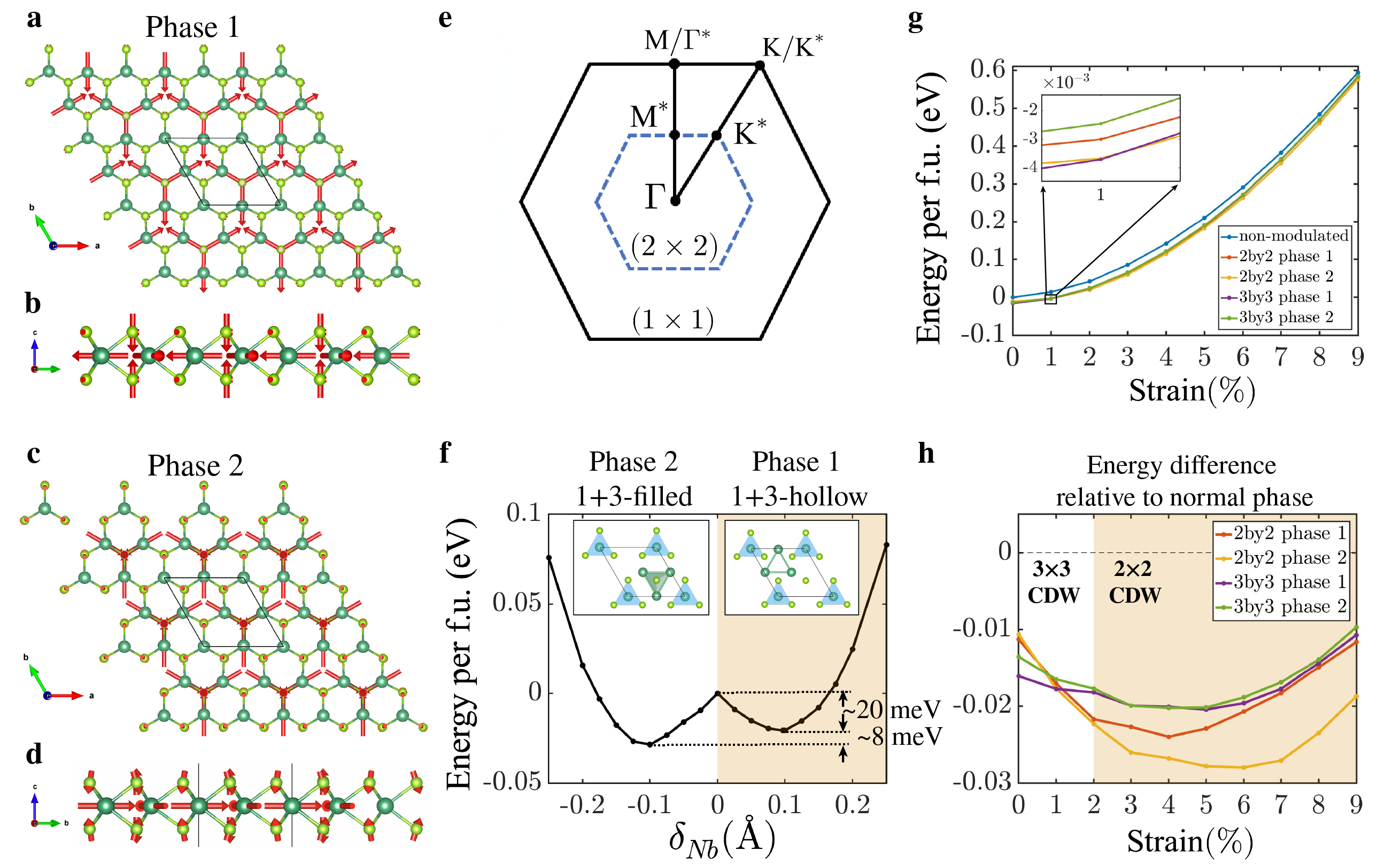
In analogy with the two known 33 phases (see SM S.3.) [43], we can label the two 22 CDW phases, shown in the insets of Fig. 2f, as 1+3-hollow (phase 1) and 1+3-filled (phase 2). The periodic lattice distortion (PLD) of phase 1 is shown in Fig. 2a (top view) and Fig. 2b (side view). Three Nb atoms on the hexagonal ring within the 22 unit cell are shifted inward to the center of the hexagonal ring, as in the breathing-in phase of a breathing mode, and form the hollow triangular Nb trimer with no Se atoms at the center. The six Se atoms on the hexagonal ring move (slightly) away from the center of the ring. All these Nb and Se atoms, which formed the hexagonal ring within the 22 unit cell, only have in-plane modulation vectors with no out-of-plane component. As shown in Fig. 2b, those Se with three Nb atoms moving away from them have the modulations purely out-of-plane toward the Nb layer.
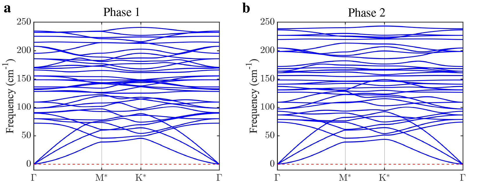
As shown in Fig. 2c-d, the PLD of second phase is also dominated by the same three Nb atoms, but now moving outward from the center of the hexagonal ring, so that three Nb from different rings all move toward the Se atom at their common corner and form a filled triangular Nb trimmer with Se atoms at the center. That is, the Nb displacements of the two CDWs resemble two distortions of a single soft Nb breathing mode phonon, 180o out of phase. Different from the first phase, there are both in-plane and out-of-plane modulation for those six Se atoms on the hexagonal ring. As shown in Fig. 2(d), the modulation of those Se atoms not on the hexagonal ring pointing outward to the Nb layer vertically with no in-plane component. To confirm structural stability, the absence of soft modes in the phonon spectrum within the 22 BZ for both phases is illustrated in SM S.2..
The stability of these two phases is further supported by the local energy landscape when changing the trio of in-plane Nb (Nb trimer) distortions manually and fully relaxing all other atoms for each set of . The distortion set is chosen to obey the symmetry of the space group. The total energy per formula unit (f.u.) at different with lattice constants under 6% strain are shown in Fig. 2f. The energy has a local maximum at (normal phase) and two inequivalent local minima at finite values of (phase 1 and phase 2), and the asymmetric double wells shape reflects the lack of inversion symmetry in monolayer -NbSe2. When cooling strained -NbSe2 through , the system can settle into either configuration with no barrier. It takes at least around 20meV (240K) to overcome the barrier and transition to the other energy well corresponding to the other 22 phase. Therefore, even though one phase is around 8meV lower than the other one, we predict these two 22 phases will coexist in a strained monolayer -NbSe2 sample, possibly forming a long range landscape, as in the 33 phases [34], which could be verified by STM.
In Fig. 2g we compare the energies of the two 22 CDW phases, two 33 CDW phases [43, 44] (see SM S.3.) and the non-CDW phase. Fig. 2h shows the differences of total energy per f.u. relative to the energy of normal phase as a function of strain. It reveals that the 33 CDW phase 1 is the ground state with 0%-1% strain, but for higher strain the 22 CDW phase 2 becomes the ground state and both phases of 22 CDW have lower energies than the 33 CDW and normal phases. The strain-induced CDW phase transition from 33 to 22 phases is consistent with the shift of soft phonon modes in Fig. 1d and the inversion of energy hierarchy in Fig. 2g. Furthermore, the competition between 22 and 33 CDW phases around 1% strain also provides an explanation for their coexistence in the STM experiment. [39]
V Electronic band structures
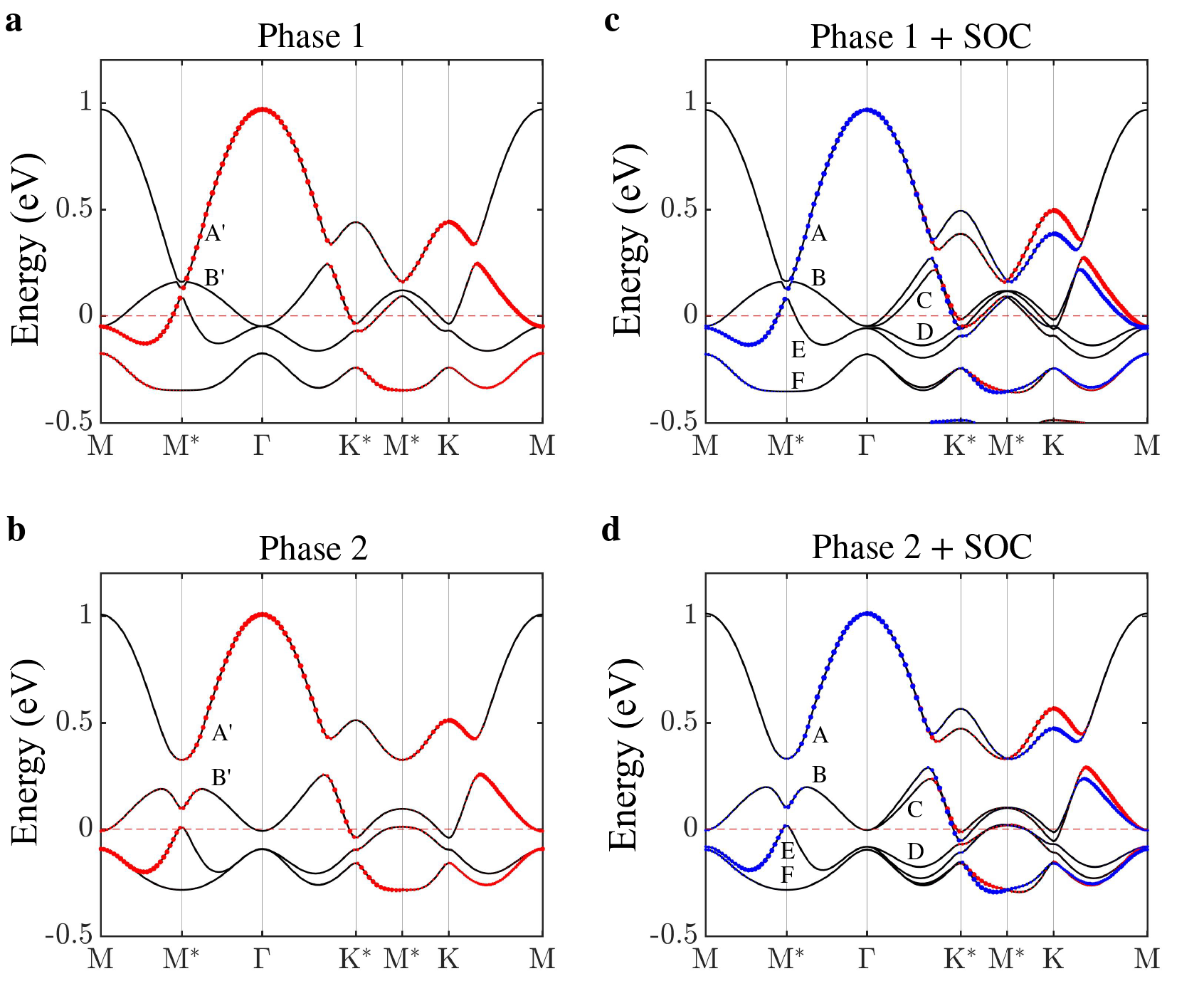
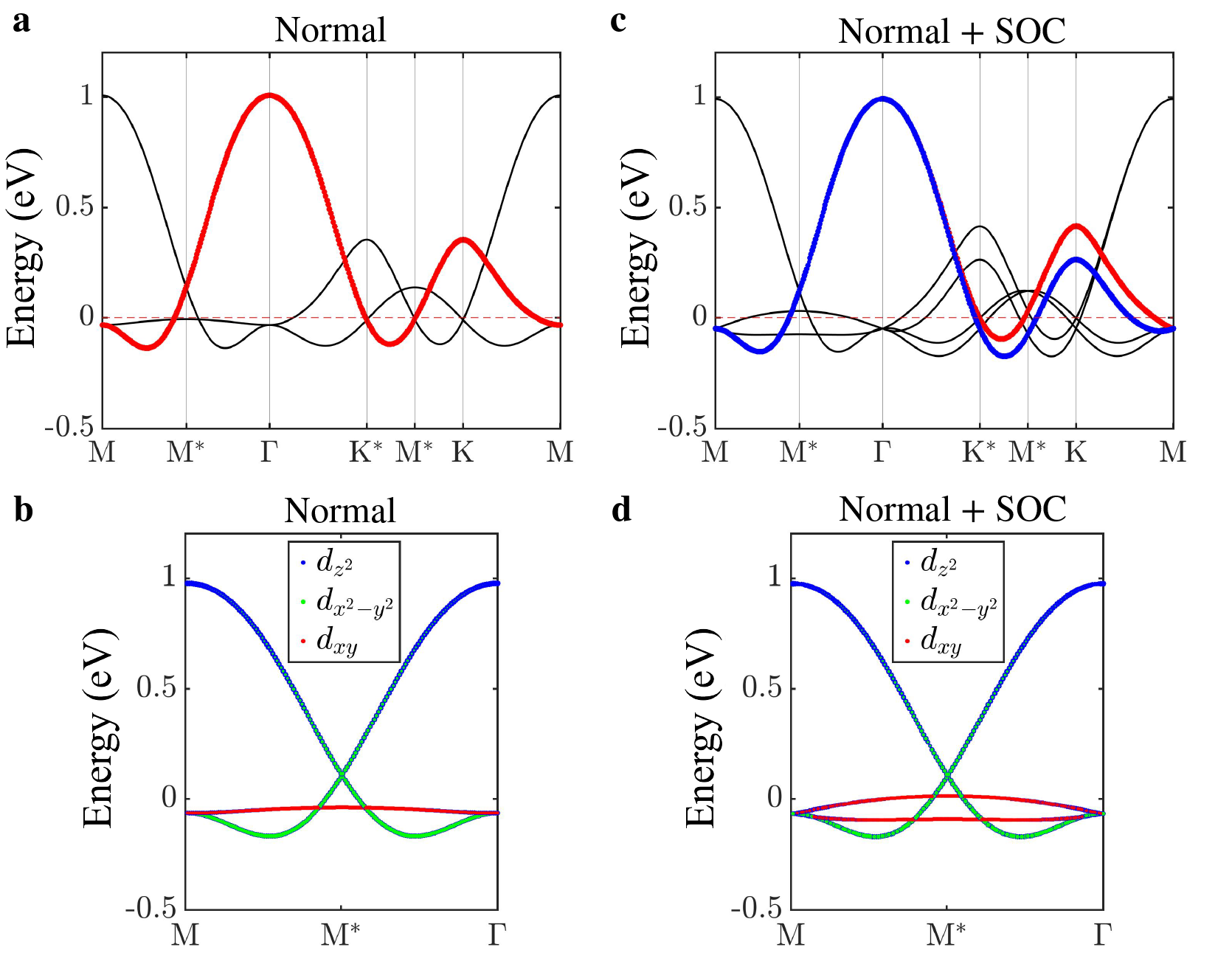
Fig. 3 shows the electronic band structures of the modulated phases under 6% in-plane biaxial tensile strain. The 22 CDW phases under different strain give rise to qualitatively similar electronic dispersions. The folded (black lines) and unfolded (markers) band structures without/with spin-orbit coupling (SOC) for phase 1 are shown in Fig. 3a/c. The unfolded bands shown by the red and blue markers reveal how the CDW modifies the normal phase band structure in the 11 BZ (See SM S.4. for the normal phase band structure). Without SOC, the band dispersion around M∗ along the -M line displays a feature of band inversion between band A′ and B′ with the inverted gap meV as shown in Fig. 4a. As shown in Fig. 4b, two Dirac nodes appear near each M∗, which is a saddle point in the band structure hosting a Van Hove singularity, due to the crystalline mirror and time-reversal symmetries. Note that for both phases, all the bands on the -M line are doubly-degenerate, which reflects the mirror line along the direction in the crystal structure as shown in Fig. 2a.
However, as shown in Fig. 4c, SOC opens a fundamental gap meV between bands A and B of phase 1 at around 0.15eV above the Fermi level. To check whether these two bands are connected away from the -M line, the 2D energy dispersion in the zoomed-in region around M∗ is shown in Fig. 4d. Bands A and B display a camelback shape near M∗, suggestive of band inversion with non-trivial band topology. From Fig. 4(c-d), it is clear that there is a full gap between bands A and B in the whole 22 BZ with fundamental gap meV and inverted gap meV.
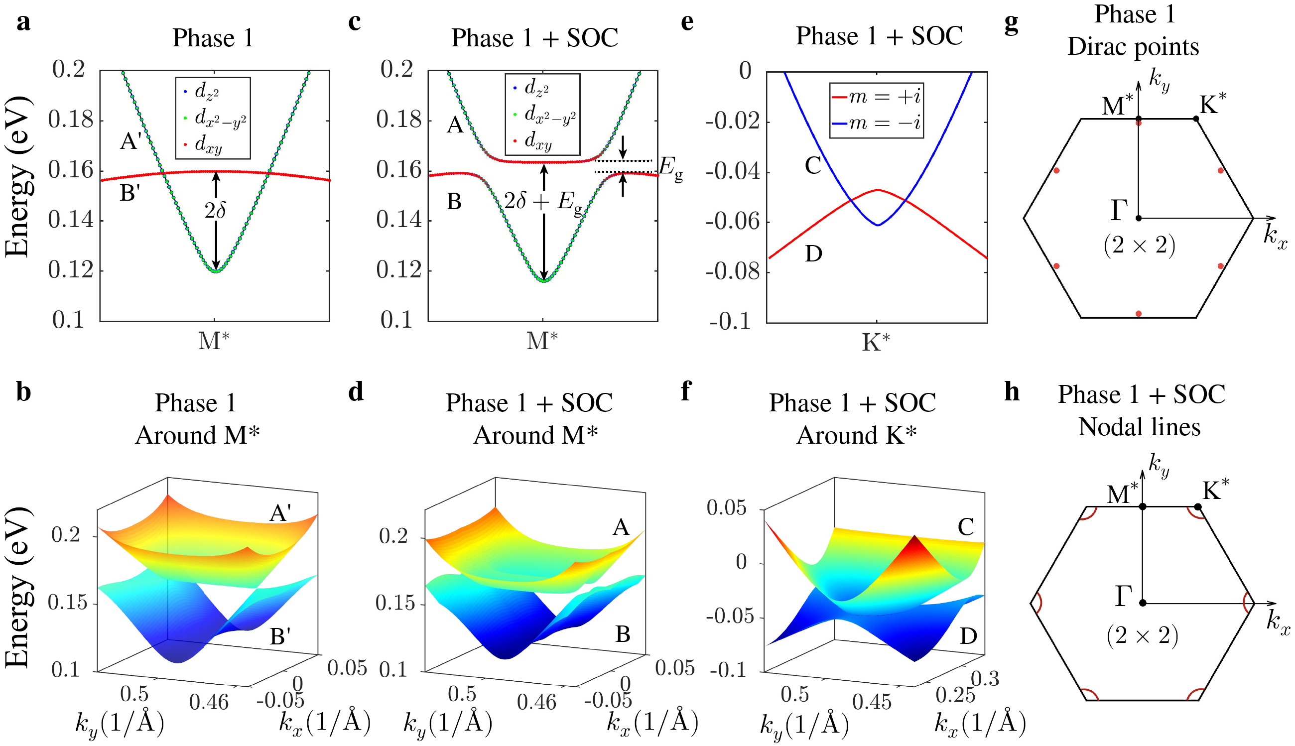
To understand the origin of the inverted band structure near M∗, we analyze the orbital character of the bands and the results are shown by the size of markers in Fig. 4a, c. There is almost no and orbital character in the bands around the Fermi level which is consistent with orbital character in the normal phase. (See SM S.4.) From Fig. 4a, without including SOC, the structural distortion and the period doubling due to PLD cause the band inversion between and a combination of and bands around M∗. Then, SOC opens the fundamental band gap between bands A and B in phase 1 without further band inversion as shown in Fig. 4c. It’s worth emphasizing that SOC doesn’t open a gap in the 22 normal phase (as shown in SM S.4.), thus the PLD due to 22 CDW phase transition is crucial in the formation of this gap.
Due to the existence of mirror symmetry in the whole 2D BZ, we can separate all the bands by their mirror eigenvalues of . For the phase 1 with SOC, there is a doubly-degenerate nodal ring around each K∗ point, formed by bands C and D with opposite mirror eigenvalues as shown in Fig. 4(e-f). Note that, between these two bands, SOC opens a small fundamental gap at and there is no other contact point besides the nodal rings.
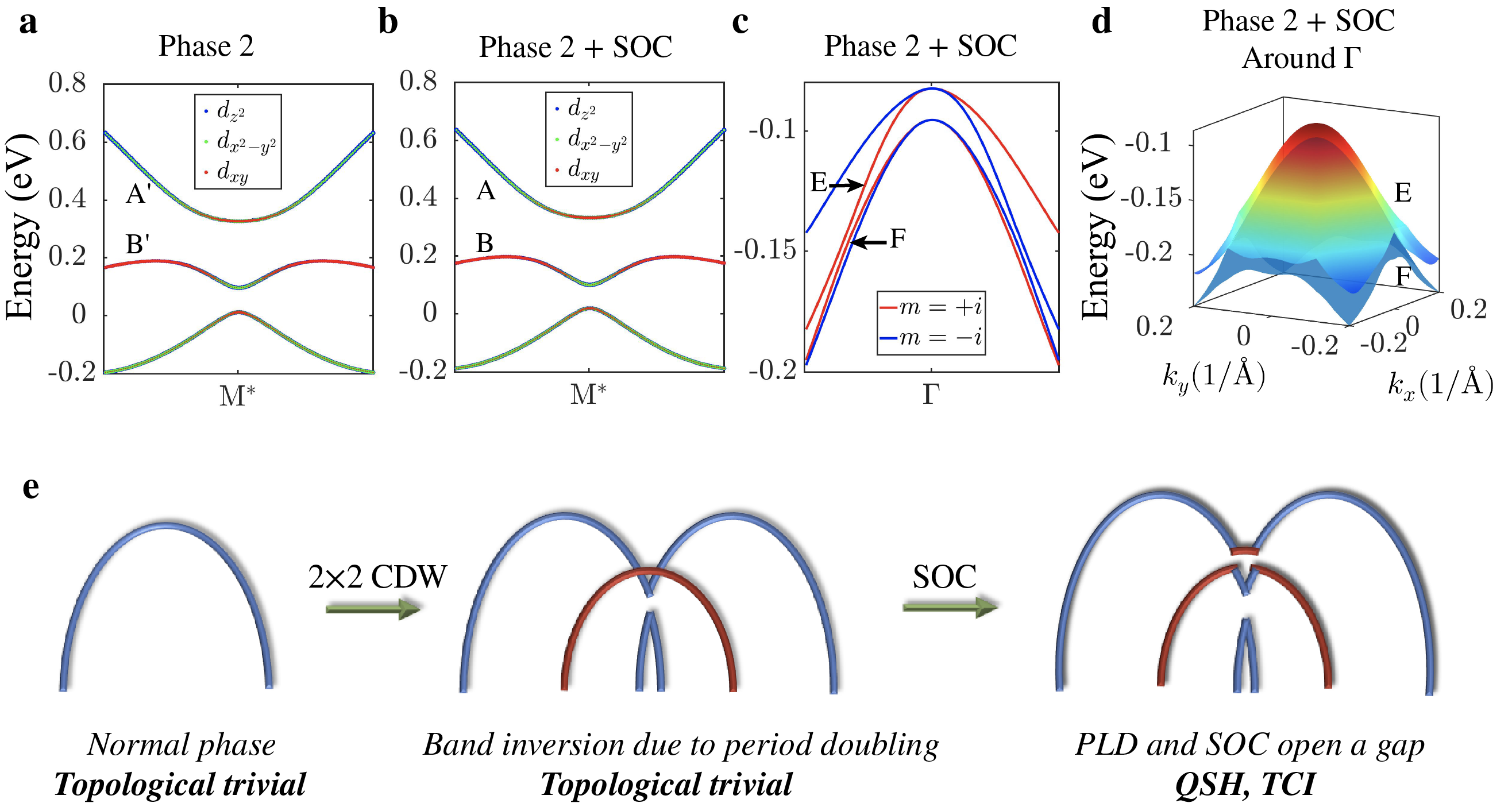
Fig. 3b/d show the unfolded band structure without/with SOC of phase 2. Unlike the band structure of phase 1, CDW opens a full gap between band A and band B even without including SOC. A band inversion feature of camelback shape near M∗ also appears in band B of phase 2. The orbital character is shown in Fig. 5a without SOC and Fig. 5b with SOC. We find that SOC plays negligible role in the band inversion around M∗ and the CDW has already double inverted the bands. Instead, as shown in Fig. 3d, SOC opens a full CDW gap between bands E and F.
The band structure between bands E and F around along K∗--K∗ is shown in Fig. 5c. Since the bands around the Fermi level are composed of Nb , and orbits which are all even under out-of-plane mirror symmetry, so the eigenvalues of these bands are consistent to the SOC induced spin splitting in the band structure. Therefore, the mirror eigenvalues of each spin-splitting pair are opposite to each other at two finite momentum and in the 2D BZ, and they exchange signs whenever they cross over the -M∗ mirror lines which are spin-degenerate lines. The 2D dispersion of bands E and F is shown in Fig. 5d to demonstrate that there is no connected point even away from the high symmetry lines around point. Besides, in contrast to phase 1, there are three full CDW gaps around the Fermi level in phase 2; There is an additional full CDW gaps between bands C and D, and therefore there is no nodal ring in phase 2.
VI Topology of the CDW phase
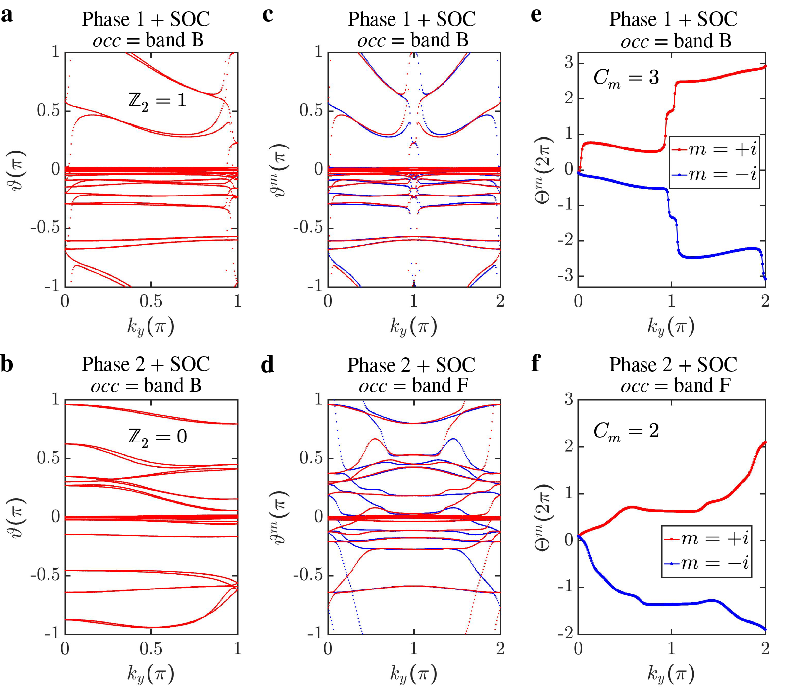
The band inversion induced by the CDW ordering indicates the possibility of non-trivial topology. Due to the existence of TRS and the full band gap between bands A and B within the folded BZ in both phases, the nature of its band topology within this CDW gap can be examined by calculating the TRS protected index. Because there is no inversion symmetry in the monolayer structure, the index is calculated by the Wilson loop method [49] and we find that for phase 1 and for phase 2 as shown in Fig. 6(a-b), indicating that the phase 1 of 22 CDW hosts the QSH insulator phase in the CDW gap.
The analysis of orbital character provides an explanation for why the index is non-trivial for phase 1 but trivial for phase 2. For phase 1 in the absence of SOC, the band inversion due to CDW leads to the appearance of an inverted gap at M∗ and six Dirac points near M∗ in the 22 BZ as shown in Fig. 4g. SOC then opens up a fundamental gap meV at these Dirac points leading to a QSH insulator. The schematic picture is shown in Fig. 5e. Since SOC cannot open the gap without the 22 CDW phase transition, the topology is purely induced from the CDW phase transition. However, for phase 2, band inversion due to the CDW has already opened a full gap without SOC, and the double band inversion of bands at M∗ leads to a trivial topology in phase 2.
The topology of nodal ring around K∗ between bands C and D in phase 1, as shown in Fig 4(e-f), is confirmed by the zero-dimensional enclosing manifold [50]. By counting the number of occupied bands with eigenvalue up to the energy of nodal ring at a point inside(outside) of the nodal ring denoted as (), the class topological invariance is defined as which corresponding to a mirror-protected TNL semimetal.
We further examine the mirror Chern number for the full CDW gaps in both phases. The Wilson loop calculation with mirror eigenvalues separation is shown in Fig. 6(c-d), and the accumulated geometric phase difference along the principle axis is shown in Fig. 6(e-f), where with as the Berry phases, as the band index and as the number of occupied bands. Since the first Chern class of the sub Hilbert space with each mirror eigenvalue is identified as , we find the mirror Chern number for phase 1 when the occupied bands are counted up to band B, and for phase 2 when the occupied bands are counted up to band F, indicating that both phases of 22 CDW coexist with the topological crystalline insulator (TCI) state. It is worth emphasizing that the 22 CDW phase 1 is a triple-topological state where both QSH and TCI states coexist in the a full CDW gap between bands A and B, and the mirror-protected topological nodal rings occur between bands C and D.
VII Conclusion
Our first-principles modeling and analysis show that the 22 CDW phase of monolayer -NbSe2 could assume two stable crystal structures. The phonon spectrum and energy hierarchy from our DFT calculations explain the coexistence of 33 and 22 triangular phases seen in experiments [39]. As a function of strain, both the shifting of the soft phonon mode and the inversion in energy hierarchy support the strain-induced CDW phase to transition from the 33 triangular phase to the 22 triangular phase. Since both of the two 22 phases are equally preferred prior to spontaneous symmetry-breaking, we predict the coexistence of these two phases in a strained monolayer of -NbSe2, which could be verified by further STM experiments.
We also predict both the 22 CDW phases we have identified to be topological. The 22 CDW Phase 1 is a triple-topological CDW phase encompassing a QSH insulator, TCI and TNL semimetal states. In contrast, the 22 CDW Phase 2 only contain the TCI state. This is the first prediction of the TCI and TNL states coexisting with a CDW. Since the unmodulated phase here is trivial, the topological phases emerge directly from the formation of charge order in the CDW. Combining our finding of the three emergent topological states, the new competing CDW phases, and the coexistence of a superconducting state [35] suggests that monolayer -NbSe2 could provide an exciting sandbox for exploring the interplay between correlation effects and topological states. It could also provide a unique materials platform for developing applications in quantum electronics and spintronics, and Majorana-based topological quantum computing.
VIII Acknowledgments
We thank Chao-Sheng Lian, for providing their 33 CDW structures in [43]. The work at Northeastern University was supported by the US Department of Energy (DOE), Office of Science, Basic Energy Sciences Grant No. DE-SC0019275 (materials discovery for QIS applications) and benefited from Northeastern University’s Advanced Scientific Computation Center and the National Energy Research Scientific Computing Center through DOE Grant No. DE-AC02-05CH11231. H.L. acknowledges the support by the Ministry of Science and Technology (MOST) in Taiwan under grant number MOST 109-2112-M-001-014-MY3. S.M. and A.A. gratefully acknowledge the HPC facility at Indian Institute of Technology Kanpur, for computational resources. J.N. benefited from resources of the Tampere Center for Scientific Computing, TCSC. T.H.’s research is supported by the ITU-BAP project TDK-2018-41181. T.-R.C. was supported by the Young Scholar Fellowship Program from the Ministry of Science and Technology (MOST) in Taiwan, under a MOST grant for the Columbus Program MOST110-2636-M-006-016, NCKU, Taiwan, and National Center for Theoretical Sciences, Taiwan. Work at NCKU was supported by the MOST, Taiwan, under grant MOST107-2627-E-006-001 and Higher Education Sprout Project, Ministry of Education to the Headquarters of University Advancement at NCKU.
IX Methodology
The lattice dynamics calculations of the unmodulated 11 structure were carried out within the framework of density functional perturbation theory (DFPT) [51] using norm-conserving pseudo-potentials [52] as implemented in the Quantum Espresso simulation package [53]. The exchange-correlation effects are treated within the local density approximation (LDA) [54] with the Perdew-Zunger parametrization [55]. We have fully optimized both the ionic positions and lattice parameters until the residual forces on each ion were less than Ry and zero-stress tensors are obtained. The monolayer is obtained from the relaxed bulk structure by setting a vacuum of 14 along the z-direction to eliminate the interaction with spurious replica images. Another ionic relaxation for monolayer structure follows this to ensure structural stability. The in-plane biaxial tensile strain is simulated by increasing the lattice parameter based on the relaxed monolayer structure. For the strained 11 structure, we only relax the atoms position by fixing the lattice parameter and unit cell shape. For normal phase, the phonon dispersion is obtained by Fourier interpolation of the dynamical matrices computed on a -mesh and mesh [6]. For the 22 CDW phase, the Brillouin zones for electronic and vibrational calculations are sampled using and respectively.
The lattice relaxation of the modulated structures and all of the electronic structure calculations were carried out within the DFT framework with the projector augmented wave (PAW) method using the Vienna ab initio Simulation Package (VASP) [56, 57, 54, 58, 59]. We used the strongly-constrained-and-appropriately-normed (SCAN) meta-generalized-gradient-approximation (meta-GGA) energy functionals with the Perdew-Burke-Ernzerhof (PBE) parametrization [60] to include exchange-correlation effects in computations. An energy cut-off of 400 eV was used for the plane-wave-basis set. To keep approximately same distance between the sampling -points, the -centered , and -mesh was employed accordingly to sample the 2D Brillouin zone (BZ) of , and monolayer structure. The ionic relaxation of modulated 22 and 33 structures is set to converge upon satisfying the condition of residual forces smaller than eVÅ-1 per atom and energy tolerance smaller than eV per unit cell. The first order Methfessel-Paxton semearing method with smearing width 0.1eV was used in the ionic relaxation process, the tetrahedron method with smearing width 0.1eV was used in the self-consistent run of electronic structure, and the Gaussian smearing with smearing width 0.1eV was used to calculate the electronic band structure along high-symmetry line. The spin-orbit coupling (SOC) is not included in the ionic relaxation process, and the SOC effects are included self-consistently in the electronic structure calculations. The topological analysis was performed by employing a real-space tight-binding model Hamiltonian, which was obtained by using the VASP2WANNIER90 interface [61]. Nb d and Se p states were included in generating Wannier functions. All crystal structures are visualized using the VESTA [62] package.
X Author contributions
W.C.C., S.M., R.M., J.N., B.S., T.H., H.L. and A.B. initiated the project. W.C.C and S.M. performed first-principles calculations and theoretical analysis with guidance from R.M., J.N., B.S., T.H., A.A., T.R.C., H.L. and A.B.. All authors discussed the results and contributed to the planning and writing the manuscript.
XI Competing financial interests
The authors declare no competing financial interests.
References
- [1] Wen, X.-G. Choreographed entanglement dances: Topological states of quantum matter. Science 363, eaal3099 (2019).
- [2] Raghu, S., Qi, X.-L., Honerkamp, C. & Zhang, S.-C. Topological mott insulators. Phys. Rev. Lett. 100, 156401 (2008).
- [3] Shi, W. et al. A charge-density-wave topological semimetal. Nature Physics (2021).
- [4] Mitsuishi, N. et al. Switching of band inversion and topological surface states by charge density wave. Nature Communications 11, 2466 (2020).
- [5] Jiang, Y.-X. et al. Discovery of topological charge order in kagome superconductor KV3Sb5 (2020). eprint arXiv:2012.15709.
- [6] Correa, L. E. et al. Multiband superconductivity and charge density waves in the topological semimetal ni-doped ZrTe2 (2021). eprint arXiv:2102.04812.
- [7] Kane, C. L. & Mele, E. J. topological order and the quantum spin hall effect. Phys. Rev. Lett. 95, 146802 (2005).
- [8] Kane, C. L. & Mele, E. J. Quantum spin hall effect in graphene. Phys. Rev. Lett. 95, 226801 (2005).
- [9] Bernevig, B. A. & Zhang, S.-C. Quantum spin hall effect. Phys. Rev. Lett. 96, 106802 (2006).
- [10] Liu, J. et al. Spin-filtered edge states with an electrically tunable gap in a two-dimensional topological crystalline insulator. Nature Materials 13, 178–183 (2014).
- [11] Wrasse, E. O. & Schmidt, T. M. Prediction of two-dimensional topological crystalline insulator in PbSe monolayer. Nano Letters 14, 5717–5720 (2014).
- [12] Jin, Y.-J. et al. The prediction of a family group of two-dimensional node-line semimetals. Nanoscale 9, 13112–13118 (2017).
- [13] Jin, L. et al. Two-dimensional weyl nodal-line semimetal in a ferromagnetic monolayer with a high curie temperature. Phys. Rev. B 102, 125118 (2020).
- [14] Niu, C. et al. Robust dual topological character with spin-valley polarization in a monolayer of the dirac semimetal . Phys. Rev. B 95, 075404 (2017).
- [15] Bernevig, B. A., Hughes, T. L. & Zhang, S.-C. Quantum spin hall effect and topological phase transition in HgTe quantum wells. Science 314, 1757 (2006).
- [16] König, M. et al. Quantum spin hall insulator state in HgTe quantum wells. Science 318, 766 (2007).
- [17] Qian, X., Liu, J., Fu, L. & Li, J. Quantum spin hall effect in two-dimensional transition metal dichalcogenides. Science 346, 1344–1347 (2014).
- [18] Tang, S. et al. Quantum spin hall state in monolayer -WTe2. Nature Physics 13, 683–687 (2017).
- [19] Fei, Z. et al. Edge conduction in monolayer WTe2. Nature Physics 13, 677–682 (2017).
- [20] Leroux, M. et al. Strong anharmonicity induces quantum melting of charge density wave in under pressure. Phys. Rev. B 92, 140303 (2015).
- [21] Flicker, F. & van Wezel, J. Charge order from orbital-dependent coupling evidenced by NbSe2. Nature Communications 6, 7034 (2015).
- [22] Zhu, X. et al. Signature of coexistence of superconductivity and ferromagnetism in two-dimensional NbSe2 triggered by surface molecular adsorption. Nature Communications 7, 11210 (2016).
- [23] Manzeli, S., Ovchinnikov, D., Pasquier, D., Yazyev, O. V. & Kis, A. 2D transition metal dichalcogenides. Nature Reviews Materials 2, 17033 (2017).
- [24] Roldán, R., Castellanos-Gomez, A., Cappelluti, E. & Guinea, F. Strain engineering in semiconducting two-dimensional crystals. Journal of Physics: Condensed Matter 27, 313201 (2015).
- [25] Shi, Y. et al. Imaging quantum spin hall edges in monolayer WTe2. Science Advances 5, eaat8799 (2019).
- [26] Zhou, Y. et al. Tensile strain switched ferromagnetism in layered NbS2 and NbSe2. ACS Nano 6, 9727–9736 (2012).
- [27] Xu, Y., Liu, X. & Guo, W. Tensile strain induced switching of magnetic states in NbSe2 and NbS2 single layers. Nanoscale 6, 12929–12933 (2014).
- [28] Zheng, F., Zhou, Z., Liu, X. & Feng, J. First-principles study of charge and magnetic ordering in monolayer . Phys. Rev. B 97, 081101 (2018).
- [29] Singh, B., Hsu, C.-H., Tsai, W.-F., Pereira, V. M. & Lin, H. Stable charge density wave phase in a -TiSe2 monolayer. Phys. Rev. B 95, 245136 (2017).
- [30] Revolinsky, E., Spiering, G. & Beerntsen, D. Superconductivity in the niobium-selenium system. Journal of Physics and Chemistry of Solids 26, 1029–1034 (1965).
- [31] Moncton, D. E., Axe, J. D. & DiSalvo, F. J. Study of superlattice formation in -Nb and -Ta by neutron scattering. Phys. Rev. Lett. 34, 734–737 (1975).
- [32] Calandra, M., Mazin, I. I. & Mauri, F. Effect of dimensionality on the charge-density wave in few-layer . Phys. Rev. B 80, 241108 (2009).
- [33] Xi, X. et al. Strongly enhanced charge-density-wave order in monolayer NbSe2. Nature Nanotechnology 10, 765–769 (2015).
- [34] Gye, G., Oh, E. & Yeom, H. W. Topological landscape of competing charge density waves in . Phys. Rev. Lett. 122, 016403 (2019).
- [35] Ugeda, M. M. et al. Characterization of collective ground states in single-layer NbSe2. Nature Physics 12, 92–97 (2016).
- [36] Wang, H. et al. High-quality monolayer superconductor nbse2 grown by chemical vapour deposition. Nature Communications 8, 394 (2017).
- [37] Xi, X. et al. Ising pairing in superconducting nbse 2 atomic layers. Nature Physics 12, 139–143 (2016).
- [38] Wickramaratne, D., Khmelevskyi, S., Agterberg, D. F. & Mazin, I. I. Ising superconductivity and magnetism in . Phys. Rev. X 10, 041003 (2020).
- [39] Gao, S. et al. Atomic-scale strain manipulation of a charge density wave. Proceedings of the National Academy of Sciences 115, 6986 (2018).
- [40] Soumyanarayanan, A. et al. Quantum phase transition from triangular to stripe charge order in nbse2. Proceedings of the National Academy of Sciences 110, 1623–1627 (2013).
- [41] Leriche, R. T. et al. Misfit layer compounds: A platform for heavily doped 2d transition metal dichalcogenides. Advanced Functional Materials 31, 2007706 (2021).
- [42] Silva-Guillén, J. Á., Ordejón, P., Guinea, F. & Canadell, E. Electronic structure of -NbSe2 single-layers in the CDW state. 2D Materials 3, 035028 (2016).
- [43] Lian, C.-S., Si, C. & Duan, W. Unveiling charge-density wave, superconductivity, and their competitive nature in two-dimensional nbse2. Nano Letters 18, 2924–2929 (2018).
- [44] Guster, B. et al. Coexistence of elastic modulations in the charge density wave state of -NbSe2. Nano Letters 19, 3027–3032 (2019).
- [45] Cossu, F., Palotás, K., Sarkar, S., Di Marco, I. & Akbari, A. Strain-induced stripe phase in charge-ordered single layer NbSe2. NPG Asia Materials 12, 24 (2020).
- [46] El-Bana, M. S. et al. Superconductivity in two-dimensional NbSe2 field effect transistors. Superconductor Science and Technology 26, 125020 (2013).
- [47] Weber, F. et al. Extended phonon collapse and the origin of the charge-density wave in . Phys. Rev. Lett. 107, 107403 (2011).
- [48] McMillan, W. L. Microscopic model of charge-density waves in . Phys. Rev. B 16, 643–650 (1977).
- [49] Soluyanov, A. A. & Vanderbilt, D. Computing topological invariants without inversion symmetry. Phys. Rev. B 83, 235401 (2011).
- [50] Fang, C., Weng, H., Dai, X. & Fang, Z. Topological nodal line semimetals. Chinese Physics B 25, 117106 (2016).
- [51] Baroni, S., Giannozzi, P. & Testa, A. Green’s-function approach to linear response in solids. Phys. Rev. Lett. 58, 1861–1864 (1987).
- [52] Troullier, N. & Martins, J. L. Efficient pseudopotentials for plane-wave calculations. Phys. Rev. B 43, 1993–2006 (1991).
- [53] Giannozzi, P. et al. QUANTUM ESPRESSO: a modular and open-source software project for quantum simulations of materials. Journal of Physics: Condensed Matter 21, 395502 (2009).
- [54] Kohn, W. & Sham, L. J. Self-consistent equations including exchange and correlation effects. Phys. Rev. 140, A1133–A1138 (1965).
- [55] Perdew, J. P. & Zunger, A. Self-interaction correction to density-functional approximations for many-electron systems. Phys. Rev. B 23, 5048–5079 (1981).
- [56] Kresse, G. & Joubert, D. From ultrasoft pseudopotentials to the projector augmented-wave method. Phys. Rev. B 59, 1758–1775 (1999).
- [57] Hohenberg, P. & Kohn, W. Inhomogeneous electron gas. Phys. Rev. 136, B864–B871 (1964).
- [58] Kresse, G. & Furthmüller, J. Efficient iterative schemes for ab initio total-energy calculations using a plane-wave basis set. Phys. Rev. B 54, 11169–11186 (1996).
- [59] Perdew, J. P., Burke, K. & Ernzerhof, M. Generalized gradient approximation made simple. Phys. Rev. Lett. 77, 3865–3868 (1996).
- [60] Sun, J., Ruzsinszky, A. & Perdew, J. P. Strongly constrained and appropriately normed semilocal density functional. Phys. Rev. Lett. 115, 036402 (2015).
- [61] Marzari, N. & Vanderbilt, D. Maximally localized generalized wannier functions for composite energy bands. Phys. Rev. B 56, 12847–12865 (1997).
- [62] Momma, K. & Izumi, F. VESTA3 for three-dimensional visualization of crystal, volumetric and morphology data. Journal of Applied Crystallography 44, 1272–1276 (2011).
Supplementary Material: Topological charge density wave in monolayer NbSe2
XII S.1. The phonon spectrum for unmodulated structure.
XIII S.2. The 22 CDW phonon spectrum.
XIV S.3. 33 CDW crystal structure of monolayer -NbSe2.
XV S.4. 22 normal phase band structure.