Optical phonon modes, static and high frequency dielectric constants, and effective electron mass parameter in cubic In2O3
Abstract
A complete set of all optical phonon modes predicted by symmetry for bixbyite structure indium oxide is reported here from a combination of far-infrared and infrared spectroscopic ellipsometry, as well as first principle calculations. Dielectric function spectra measured on high quality, marginally electrically conductive melt grown single bulk crystals are obtained on a wavelength-by-wavelength (a.k.a. point-by-point) basis and by numerical reduction of a subtle free charge carrier Drude model contribution. A four-parameter semi-quantum model is applied to determine all sixteen pairs of infrared-active transverse and longitudinal optical phonon modes, including the high-frequency dielectric constant, . The Lyddane-Sachs-Teller relation then gives access to the static dielectric constant, . All experimental results are in excellent agreement with our density functional theory calculations and with previously reported values, where existent. We also perform optical Hall effect measurements and determine for the unintentionally doped -type sample a free electron density of cm-3, mobility of cm2/(Vs), and an effective mass parameter of . Density and mobility parameters compare very well with results of electrical Hall effect measurements. Our effective mass parameter, which is measured independently of any other experimental technique, represents the bottom curvature of the point in In2O3 in agreement with previous extrapolations. We use terahertz spectroscopic ellipsometry to measure the quasi-static response of In2O3, and our model validates the static dielectric constant obtained from the Lyddane-Sachs-Teller relation.
I Introduction
Indium oxide (In2O3) is a sesquioxide of continued interest as a part of the broader transparent semiconducting oxide family. In2O3 crystallizes in a stable phase with bixbyite structure and cubic crystal symmetry. Similarly to other transparent semiconducting oxides, In2O3 is classified as a wide bandgap (2.9 eV) material.King et al. (2009) When doped with tin, In2O3 shows high electrical conductivity.Bel Hadj Tahar et al. (1998); Shigesato, Takaki, and Haranoh (1992); Bierwagen and Speck (2014) These properties lend In2O3 to applications in transparent electrodes, Minami (2005); Lungenschmied et al. (2007); Diniz (2011); Kim et al. (2009) gas sensing,Bartic et al. (2007); Tischner et al. (2008); Kannan et al. (2010) nanowire technology,Nguyen et al. (2004) high-voltage transistors,Nayak et al. (2013); Han, Herman, and Chang (2011); Kim et al. (2016) Schottky diodes,Sheu et al. (1998); Zhang et al. (2015) and ultra-violet light emitting devices,Wei et al. (2010); Gao et al. (2011); Ouacha, Kleineberg, and Albrithen (2017); Chen, Tien, and Liao (2011) for example.
In2O3 with high structural quality has been produced by thin film and bulk growth methods. Most existing works study thin film samples and as a result, most of the applications are designed around thin film samples as well.Nagata (2019) Bierwagen and Speck reported high quality thin films grown by plasma-assisted molecular beam epitaxy (PAMBE);Bierwagen and Speck (2014); Bierwagen (2015) Yang et al. reported similarly high quality thin films grown by metal organic vapor phase epitaxy;Yang et al. (2008) and Karim, Feng, and Zhao reported high quality thin films grown by low pressure chemical vapor deposition,Karim, Feng, and Zhao (2018) for example. Recently, Galazka et al. developed a high quality single crystal bulk growth method, and thereby provided substrates with large surface areas for epitaxy.Galazka et al. (2013a) The structural quality of epitaxial layers grown, e.g., by PAMBE, is typically higher than for polycrystalline films and lower than or comparable to bulk crystals. With increasing availability of bulk samples, the possibilities for homoepitaxial and heteroepitaxial growth are becoming abundant.Sadofev et al. (2012); Liu et al. (2019)
In2O3 is commonly type and unintentionally doped (UID). High quality thin films and bulk crystals, UID and doped with tin, were investigated recently by Feneberg et al.Feneberg et al. (2016) The free electron density varied from cm-3 and can be well controlled. Electrically insulating high quality single crystalline In2O3 has not yet been reported.
The effective conduction band mass parameter in In2O3 has been widely studied. Reported effective mass values range from 0.13-0.55 ( is the free electron mass),Feneberg et al. (2016); De Wit, Van Der Bom, and De Groot (1978); Preissler et al. (2013); Weiher (1962) with rather large spread among results from experimental and theoretical investigations. Experimental results were reported from combined electrical Hall effect and Seebeck effect measurements,De Wit, Van Der Bom, and De Groot (1978); Preissler et al. (2013); Weiher (1962) combined electrical Hall effect and infrared ellipsometry measurements,Feneberg et al. (2016) and angle resolved photoemission measurements.Scherer et al. (2012); Zhang et al. (2011) Many reports of conduction band mass parameters exist which were obtained from first principle calculations in various approximations.Peelaers, Kioupakis, and Van de Walle (2019); Karazhanov et al. (2007); Fuchs and Bechstedt (2008); Odaka et al. (1997); Brewer and Franzen (2004) Perhaps the most accurate theory result was provided by Fuchs and BechstedtFuchs and Bechstedt (2008) using first principles density functional theory (DFT) calculations with nonlocal potential resulting from a HSE03 hybrid functional and quasi-particle correction. For the bcc polymorph, the effective electron mass at the point is almost direction independent and amounts to 0.22 using the HSE03 functional.Fuchs and Bechstedt (2008) The conduction band is nonparabolic, with smaller nonparabolicity than in InN but remains non-negligible.Hofmann et al. (2008) Fuchs and Bechstedt gave an approximation for the conduction band
| (1) |
where and the direct bandgap energy is obtained from calculations. The nonparabolicity of the effective mass, i.e., its dependence, can be determined by matching calculated band structure data against Eq. 1, which permits one to obtain when considering that the inverse of the second derivative of the left side in Eq. 1 is related to the -dependent effective mass parameter
| (2) |
where denotes the effective mass at .Fuchs and Bechstedt (2008) According to Fuchs and BechstedtFuchs and Bechstedt (2008) the effective mass raises to approximately 0.3 for free electron densities exceeding 1020 cm-3 in agreement with experimental investigations. Feneberg et al. used a method combining infrared ellipsometry and electrical Hall effect measurements, introduced by Kasic et al.Kasic et al. (2000) for GaN thin films, and reported effective mass parameters for type In2O3 bulk samples and epitaxial thin films with free electron densities ranging from cm-3.Feneberg et al. (2016) A strong variation of the effective mass parameter was observed with carrier density, from 0.18 for the lowest detectable carrier density to approximately 0.44 at cm-3, and explained by near point conduction band nonparabolicity. A similar conduction band nonparabolicity was observed previously for wurtzite structure InN, where the effective mass varies from 0.05 for perpendicular polarization and 0.037 for parallel polarization at the band bottom to 0.15 for both polarization directions when approaching free electron densities of 1020cm-3.Hofmann et al. (2008) A simplified approximation for the free electron density dependence of the conduction band mass was reported by Feneberg et al.
| (3) |
and matching experimental data resulted in the zero density effective mass parameter m0 and nonparabolocity parameter eV-1. The zero density effective mass value extrapolated using Eq. 3 is in very good agreement with the point effective mass from HSE03 results in Fuchs and Bechstedt.
The electrical mobility decreases with increasing carrier concentration due to impurity scattering and electron-electron interactions. In2O3 single crystals grown from melt have been studied systematically using different heat treatments at temperatures from 200∘C to 1400∘C.Galazka et al. (2013b) Annealing under non-reducing conditions lead to free electron densities in the 1017 cm-3 range. Typical electron mobility parameters were reported between 140-180 cm2/(Vs). Such annealed samples revealed transmittance spectra with sharp absorption edge at 440 nm wavelength with high transparency in the visible range.Galazka et al. (2013b) A new crystal growth technique, “Levitation-Assisted Self-Seeding Crystal Growth Method” with subsequent annealing in O2-containing atmosphere resulted in improved electron mobility of 190 cm2/(Vs) in the low 1017 cm-3 free electron density range.Galazka, Uecker, and Fornari (2014) Comparison between mobility obtained from electrical Hall effect measurements and broadening parameter showed very good agreement between free electron mobility determined by infrared ellipsometry and electrical Hall effect measurements. It is noted that in this comparison performed by Feneberg et al.,Feneberg et al. (2016) electrical mobility is obtained by the same measurement which determines the electron density, and which in turn was used there to determine the effective mass.
In2O3 is known to develop a surface charge accumulation similarly to indium nitride.Darakchieva et al. (2009); Nagata et al. (2016, 2019) It has been posed that this is caused by oxygen vacancies.Walsh (2011) Additionally, Scherer et al. showed that bulk In2O3 crystals cleaved in ultra-high vacuum did not show any electron accumulation layer.Scherer et al. (2016) While this effect is necessary for applications in gas sensing, it hinders performance of transistor and diode technologies and must be controlled.
An early vibrational study by White and Keramidas of infrared and Raman spectra from powder In2O3 revealed limited sets of mode parameters. Only 11 out of the 16 transverse optical (TO) mode frequencies and none of the longitudinal optical (LO) mode frequencies were reported.White and Keramidas (1972) Hamberg and Granqvist, in a large study of sets of indium oxide thin films obtained by evaporation, reported on similar subsets of data.Hamberg and Granqvist (1986) Analysis of reflectance measured on pellet samples by Sobatta et al. added the LO mode parameters for the 11 TO mode parameters identified earlier.Sobotta et al. (1990) More recently, thin-film samples have been studied and a complete set of Raman modes have been described.Garcia-Domene et al. (2012); Kranert, Schmidt-Grund, and Grundmann (2014) Infrared ellipsometry was used by Feneberg et al. on a large set of samples in the spectral range above 300 cm-1. Highly accurate TO mode frequencies for a subset of 8 modes from the 11 modes already characterized by Sobatta et al. and White and Keramidas were reported. The LO mode parameters were not determined and the focus was directed to determine Drude model parameters for the differently doped samples in order to determine the density dependence of the effective mass parameters.
Phonon mode parameters obtained from first principles calculations are not available in the literature.
Hamberg and Granqvist determined the static dielectric constant () and the high frequency dielectric constant () from analysis of broadband reflection and transmission data obtained from polycrystalline thin films deposited by e-beam evaporation.Hamberg and Granqvist (1986) No other experimental results for the static dielectric constant appears to be available. Typical capacitance measurement configurations for radio frequency determination of the static dielectric constant require highly insulating material which has not been grown yet. Therefore, capacitance measurements, e.g., as reported for insulating -Ga2O3 are not available for In2O3.Fiedler et al. (2019) Zhang et al. obtained from DFT calculations.Zhang et al. (2011) Walsh et al. determined using interatomic potential calculations.Walsh et al. (2009) The high frequency dielectric constant is mostly agreed upon both by experiment (e.g., Feneberg et al.: )Feneberg et al. (2016) and theory (e.g., Fuchs and Bechstedt: 4.0).Fuchs and Bechstedt (2008) With the Lyddane-Sachs-Teller relationship,Lyddane, Sachs, and Teller (1941)
| (4) |
and knowledge of all infrared active transverse (TO; ) and longitudinal optical (LO; ) phonon modes and accurate value of , can be determined. However, as discussed above only 11 out of the phonon mode pairs, and , are known so far, while for neither experimental nor theoretical results seem to exist.
In this work, we report a combined terahertz, far-infrared, and infrared spectroscopic ellipsometry, optical Hall effect, and density functional theory investigation. We perform and analyze measurements on a high quality, unintentionally doped, marginally electrically conductive single crystal of cubic In2O3. We obtain and report the static dielectric constant, the optical phonons, and the free charge carrier properties. We observe and determine all remaining TO and LO phonon mode parameters from our ellipsometry measurements. We also report the complete set of zone center optical phonon modes from our theoretical investigation. We report the static dielectric constant from the full set of optical phonon modes and the Lyddane-Sachs-Teller relation. We further demonstrate excellent agreement with our LST extrapolation by comparing model-calculated with measured THz ellipsometry measurements. Our optical Hall effect measurements reveal density, , mobility, , and effective mass parameters which determine an independently measured experimental value closest to the zero density effective mass parameter, . We compare our results where available with previous reports, and we compare and discuss our optical Hall effect with electrical Hall effect results.
II Theory
II.1 Crystal Structure and Symmetry
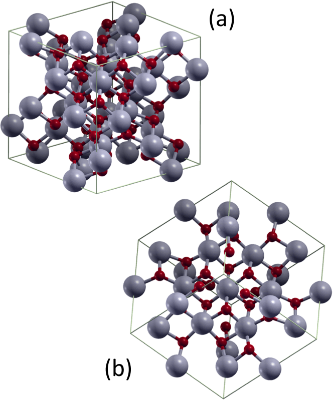
In2O3 crystallizes in the cubic bixbyte structure (space group No. 206, ). The primitive cell contains 40 atoms, which results in the total of 117 optical phonon modes, which at the Brillouin-zone center belong to the irreducible representation:
and modes are double- and triple-degenerate, respectively. Modes , , and (g - gerade) are Raman-active; modes are IR-active (and the focus of the present study); and modes and (u - ungerade) are silent.
II.2 Density Functional Theory
DFT calculations were performed by a plane wave DFT code Quantum ESPRESSO (QE).[QuantumESPRESSOisavailablefromhttp://www.quantum-espresso.org.Seealso:]GiannozziJPCM2009QE We used the local density approximation exchange-correlation functional of Perdew and Wang (PW)Perdew and Wang (1992, 2018) and optimized norm-conserving Vanderbilt (ONCV) scalar-relativistic pseudopotentials.van Setten et al. (2018) As the starting point, we used structural parameters from the Materials Project.Jain et al. (2013); Project [doi: 10.17188/1198812] The initial structure was first relaxed to force levels less than 10-6 Ry Bohr-1. A regular shifted Monkhorst-Pack grid was used for sampling of the Brillouin zone.Monkhorst and Pack (1976) A convergence threshold of Ry was used to reach self-consistency with the electronic wavefunction cutoff of 120 Ry. The relaxed cell was used for subsequent phonon calculations. The phonon frequencies, Born effective charges, and IR intensities were computed at the -point of the Brillouin zone using density functional perturbation theory, Baroni et al. (2001) as implemented in the Quantum ESPRESSO package, with the convergence threshold for self-consistency of Ry. The parameters of the TO modes were obtained from the dynamical matrix computed at the -point. The parameters of the LO modes were obtained by setting a small displacement from the -point in order to include the long-range Coulomb interactions of Born effective charges in the dynamical matrix (the so called non-analytical terms). Mode displacement patterns were rendered using XCrysDen [][.Codeavailablefromhttp://www.xcrysden.org.]Kokalj1999 running under Silicon Graphics Irix 6.5.
II.3 Spectroscopic Ellipsometry
Spectroscopic ellipsometry is a non-invasive and non-destructive measurement technique which measures the change in polarization of light () caused by interaction with the sample. In reflection ellipsometry this change is described by
| (5) |
where and are the Fresnel reflection coefficients for the light polarized parallel (p) to and perpendicular (s) to the plane of incidence. The rotation of the light’s polarization state about the axis of propagation is defined as and the relative phase shift between the parallel and perpendicular components is defined as . Hence, for each wavenumber, angle of incidence, and sample position a (, ) pair is measured.
II.4 Four-Parameter Semi-Quantum Model
To fit for the parameters describing each phonon mode found in the dielectric function, the four-parameter semi-quantum (FPSQ) model first described by Gervais and Periou can be used.Gervais and Piriou (1974); Schubert (2004) This model allows one to fit directly for TO and LO mode frequencies, and , and the determination of their independent broadening parameters, and , respectively
| (6) |
and is the high-frequency dielectric constant.Schubert (2004) The product runs over all phonons (TO-LO pairs) with symmetry. The Lyddane-Sachs-Teller (LST) relationLyddane, Sachs, and Teller (1941) in Eq. 4 then permits calculation of the static dielectric constant, using all other parameters in Eq. 6 determined from analysis of the wavenumber-by-wavenumber obtained .
II.5 Drude Free Charge Carrier Model
The FPSQ model is further modified to account for free charge carrier contributions via the addition of a Drude term:Schubert (2004)
| (7) |
where is the plasma frequency
| (8) |
and where , , and describe the free charge carrier volume density, the effective mass, and the plasma broadening parameter, respectively. From the plasma broadening parameter, the optical mobility parameter, , can be found via:
| (9) |
II.6 Optical Hall Effect
The optical Hall effect experiment and analysis procedure is summarized by Schubert et al.Schubert et al. (2016) Derived from the equation of motion, the dielectric function component for free charge carriers under the effect of an external magnetic field can be written as follows:
| (10) |
Here, is the cyclotron frequency
| (11) |
Note that the signature of depends on the type of the free charge carriers and hence, the signs of the optical Hall effect data reveal or type conductivity.Schubert et al. (2016) The external magnetic field is given in the ellipsometer coordinate system (x,y,z) as where . The optical Hall effect experiment gives access to the cyclotron frequency, therefore, if plasma frequency and broadening parameters are known from zero-field ellipsometry measurements, , , and can all be determined independently from each other, and without use of an additional separate experiment, e.g., an electrical Hall effect measurement. One further has the opportunity to compare density and mobility parameters obtained from optical and electrical techniques. It is noteworthy to point out the very different mechanisms of transport which are tested in an optical and in an electrical measurement. For a traditional electrical Hall configuration, for example, transport and scattering phenomena are collected over macroscopic distances across the sample; while for optical measurements, the lateral displacement of the free charge carriers is on the order of nanometers. In an ideal crystal without defects, both techniques will determine very similar if not the same results.
In these optical Hall effect experiments, the ellipsometry data are recorded using the Mueller matrix convention as opposed to the and convention for the zero magnetic field measurements. The Mueller matrix formalism allows accurate capture of the small optical birefringence induced by the optical Hall effect which are then observable in the off-diagonal Mueller matrix elements. The Mueller matrix is used to describe the sample interaction with incoming light described by a Stokes vector as follows:
| (12) |
Here, the elements of the Stokes vector are defined as , , , . In this definition, , , , , , and are the intensities for the -, -, +45∘, -45∘, right handed, and left handed circularly polarized light components, respectively. Fujiwara (2007)
III Experiment
III.1 Crystal Growth
The investigated crystal sample was prepared from a bulk crystal grown from the melt by a novel technique ”Levitation-Assisted Self-Seeding Crystal Growth Method,” as described in detail elsewhere.Galazka et al. (2013a) The free electron concentration was determined from electrical Hall measurements to be cm-3, and the Hall electrical mobility is 158 cm2/(Vs) (resistivity 0.15 cm) The crystal with surface area of mm2 and thickness of 500 m with (111) surface orientation was annealed in air at temperatures of 1000∘C for 40 h. Processes for annealing and control of electron density have been reported previously.Galazka et al. (2013a) The full width at half maximum (FWHM) of the rocking curves of (222) reflexes was 30 arc sec. The investigated crystal samples were epi-ready polished. The sample was then investigated by ellipsometry and optical Hall effect without further treatment.
III.2 Far-infrared and Infrared Ellipsometry
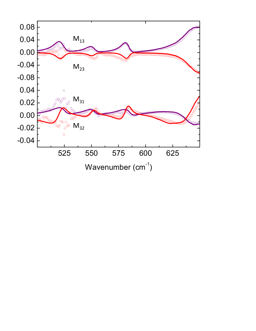
The spectra were measured at room temperature in ambient conditions on two different ellipsometer instruments. The infrared spectral range (650 - 3000 cm-1) was measured on a commercial variable angle of incidence spectroscopic ellipsometer (IR-VASE Mark-II; J.A. Woollam Co., Inc.). The far-infrared spectral range (50 - 650 cm-1) was measured on an in-house built FIR-VASE instrument.Kühne et al. (2014) Measurements were performed at = 50∘, 60∘, and 70∘ angles of incidence. Multiple azimuthal rotations were not necessary, though they were performed to ensure the cubic symmetry of the optical response. Only one azimuthal rotation is included in this analysis since all rotational data are in excellent agreement with each other. Exemplary experimental data in the FIR range is shown in Fig. 7.
III.3 Optical Hall Effect Experiment
The same sample was then mounted in our in-house optical Hall effect setup as described by Kühne et al.Kühne et al. (2014) Due to the window setup of the superconducting magnet, the angle of incidence is limited to only = 45∘. The optical Hall effect was measured in the far-infrared and in the infrared range. Measurements were taken at zero field, at T, and at T with the sample maintained at room temperature throughout the measurements. The magnetic field was oriented parallel to the incoming beam with the magnetic field strength perpendicular to the sample surface for all measurements.
III.4 Terahertz Ellipsometry
To further investigate the dielectric constants and free charge carrier contributions at quasi-static conditions, ellipsometry was measured in the THz spectrum from 670-900 GHz. The THz ellipsometer is an in-house built instrument operating in the rotating analyzer configuration allowing the measurement of the upper left Mueller matrix elements. Further information on the instrument can be found in Kühne et al.Kühne et al. (2014) Data from this instrument is shown in Fig. 10.
IV Results
IV.1 Density Functional Theory Calculations
| Mode | ||||
|---|---|---|---|---|
| (cm-1) | (cm-1) | () | () | |
| Tu-1 | 588.61 | 611.35 | 6.284 | 94.215 |
| Tu-2 | 553.45 | 569.28 | 5.686 | 33.028 |
| Tu-3 | 527.83 | 540.15 | 6.272 | 17.549 |
| Tu-4 | 460.07 | 503.84 | 0.075 | 46.718 |
| Tu-5 | 409.12 | 460.01 | 48.867 | 0.060 |
| Tu-6 | 386.87 | 394.19 | 6.593 | 1.829 |
| Tu-7 | 363.37 | 383.47 | 75.398 | 0.888 |
| Tu-8 | 330.41 | 339.21 | 37.789 | 0.919 |
| Tu-9 | 310.89 | 312.26 | 6.310 | 0.141 |
| Tu-10 | 260.02 | 260.09 | 0.139 | 0.011 |
| Tu-11 | 214.71 | 216.00 | 1.816 | 0.217 |
| Tu-12 | 171.00 | 171.29 | 0.297 | 0.042 |
| Tu-13 | 152.81 | 152.85 | 0.038 | 0.006 |
| Tu-14 | 148.44 | 148.48 | 0.038 | 0.006 |
| Tu-15 | 123.27 | 123.32 | 0.031 | 0.005 |
| Tu-16 | 100.86 | 100.86 |
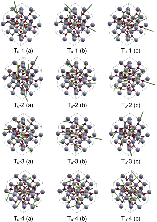
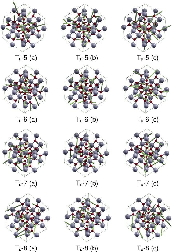
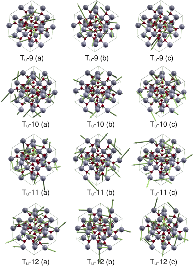
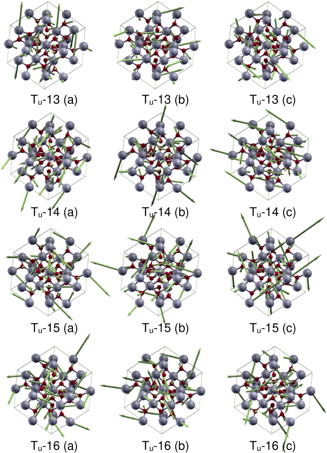
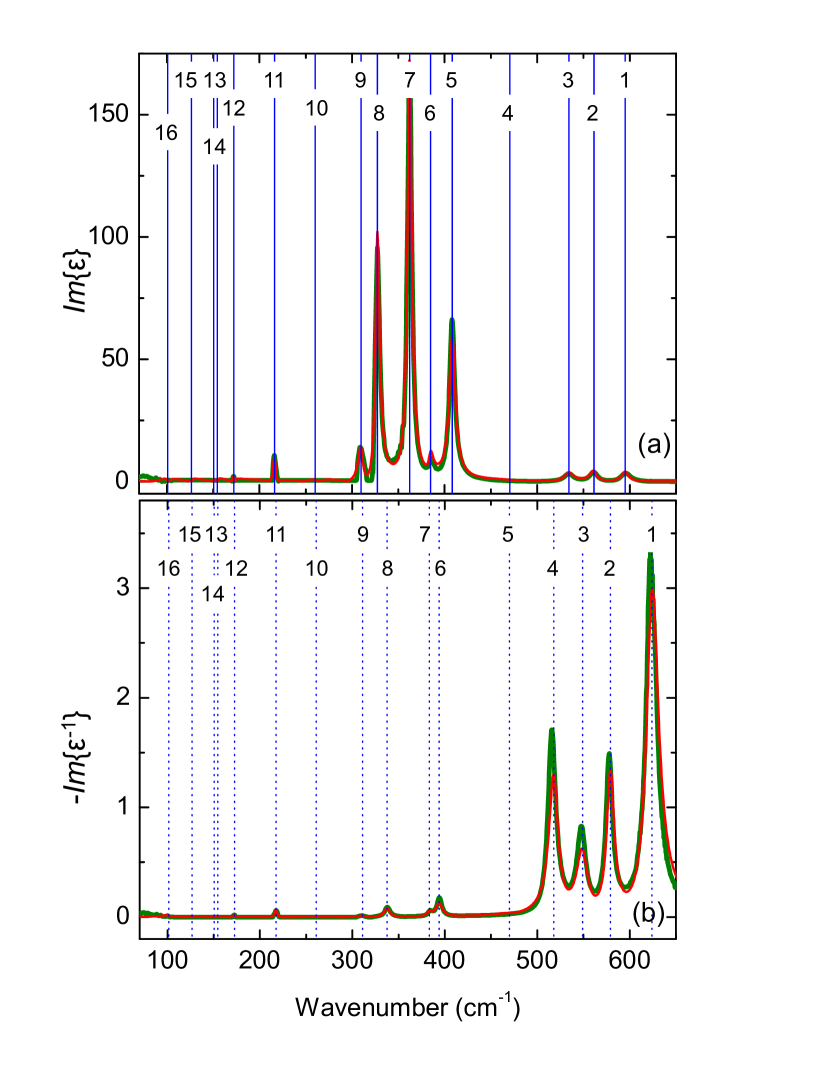
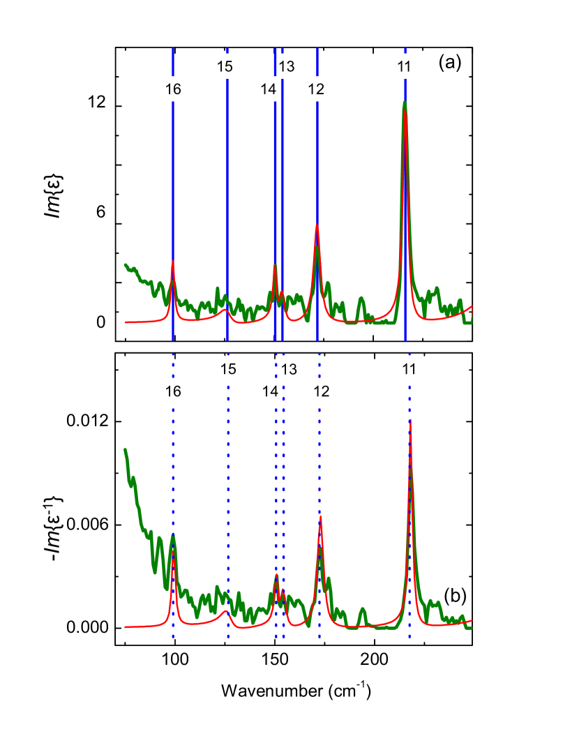
The parameters of the DFT-calculated TO and LO phonon modes are listed in Table 1 and labelled by . Renderings of the atomic displacement pattern for the TO modes are shown in Fig. 2 (modes Tu-1 to Tu-4), Fig. 3 (Tu-5 to Tu-8), Fig. 4 (Tu-9 to Tu-12), and Fig. 5 (Tu-13 to Tu-16). Because every Tu mode is triple degenerate, three eigenvectors with labels , , and are shown for every phonon mode. The corresponding transition dipoles for each such triplet are mutually orthogonal. We note that we observe 16 mode pairs as predicted by group theory. We also note that the intensities of the TO and LO modes are very small for modes 13-16 which may explain why these modes remain undetected thus far.
IV.2 Phonon Mode Analysis from Ellipsometry Data
To perform this analysis, WVASE32TM (J.A. Woollam Co., Inc.) software was utilized. We assume no finite nanometer-scale surface roughness as such roughness does not contribute to the ellipsometric data in the infrared and far-infrared spectral regions.Schubert (2004) It is worth noting here that if a surface accumulation layer had been present on this sample, it was not observable in optical Hall effect measurements nor in our zero field spectroscopic ellipsometry measurements. Initial analysis is done using a wavenumber-by-wavenumber approach where a model dielectric function is allowed to fit for each wavenumber independently to find a best-match model of the real and imaginary dielectric values. In a subtle modification to this approach, we also added a free charge carrier contribution to the model dielectric function, according to Eq. 7. This step is performed to reduce the otherwise small increase in the imaginary part of towards the far-infrared spectral range, which is caused by the absorption of the low density free electrons present in our sample. The resulting Drude model parameters will be discussed further below. The resulting dielectric function with added free charge carrier contributions lead to the therefrom calculated Mueller matrix data which excellently match with the experimental data in Fig. 6. Selected experimental and best-model calculated data in the far-infrared spectral region emphasizing small yet distinct signatures of phonon modes unidentified previously in the long wavelength range are shown in Fig. 7.
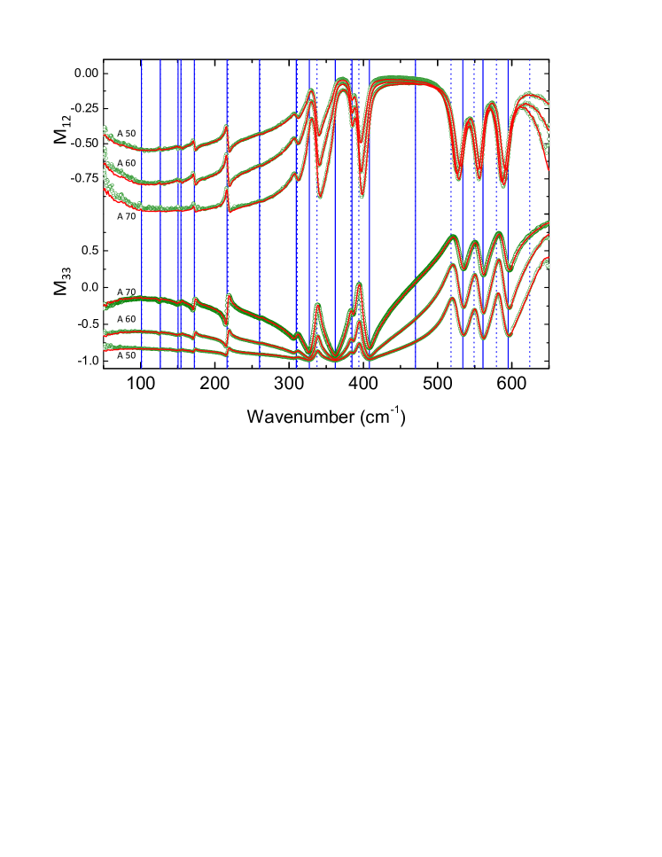
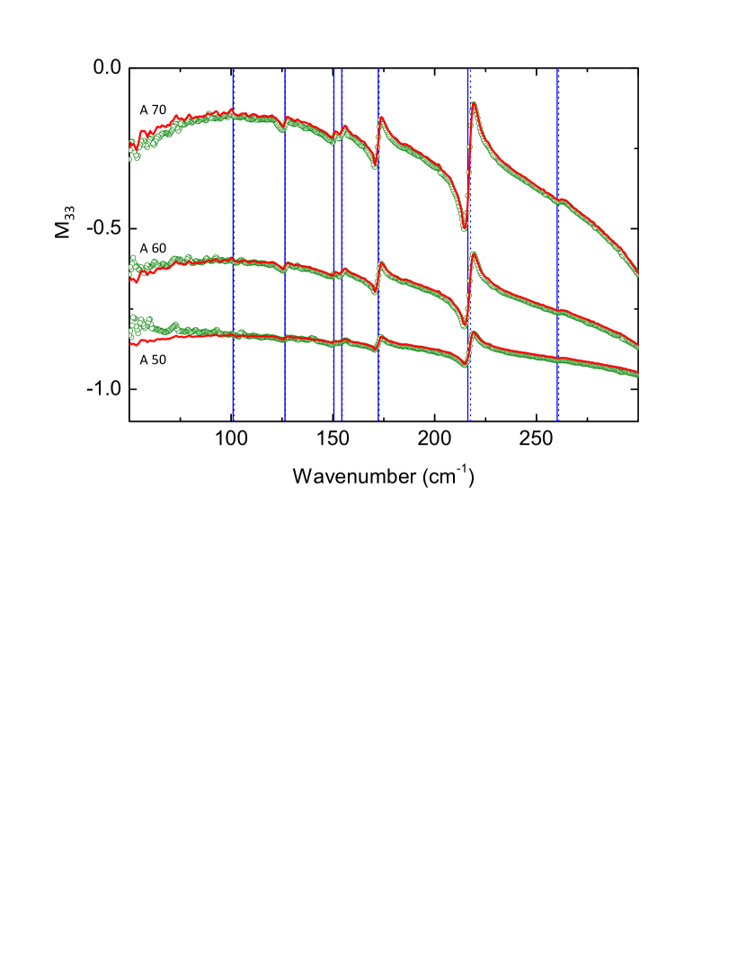
Figure 8 summarizes the wavenumber-by-wavenumber best-model parameter and Fig. 9 emphasises the far-infrared spectral region. We were then able to best-model match the dielectric function using the FPSQ model in Eq. 6. Implementing sixteen TO-LO pair parameters and we were able to find excellent agreement between the best-match model and the wavenumber-by-wavenumber produced dielectric function, as shown in Fig. 8. Note that we present the imaginary parts of and since these immediately reveal frequency and broadening of the TO and LO mode parameters, as one can assess from Eq. 6. We note further that small additional features in the far-infrared range, Fig. 9, are most likely due to noise increasing rapidly for wavenumbers below 100 cm-1 towards the THz range, best seen in Fig. 7. This noise is due to the loss of detected intensity in the far-infrared probe beam. All best-match model parameters and uncertainties are summarized in Table 2. We identify all mode pairs predicted by our DFT calculations and their broadening parameters. We note that the generalized Lowndes condition is fulfilled, where the sum of all LO broadening parameters is larger or equal to the sum of all TO broadening parameters.Kasic et al. (2000) While several modes are small in the lower spectral range, they remain detectable and were able to be fit for with limited interference. All modes are indicated in Fig. 8. Values which were range limited are designated in Table 2 with an asterisk and as a result have very large uncertainty. This can be attributed to the small magnitude of the modes (seen in the DFT analysis as well) and growing noise in the lower spectral range.
Also shown in Table 2 are previously reported TO phonon frequencies as found by Feneberg et al.Feneberg et al. (2016) and TO and LO mode frequencies as observed by Sobotta et al.Sobotta et al. (1990) Our values are in excellent agreement with the eight TO modes determined by Feneberg et al., except for the small mode T, which was not observed there. Also, Feneberg et al. did not determine any LO mode parameters, and modes below 300 cm-1remained inaccessible. The phonon modes reported by Sobotta et al. is the most comprehensive data set to date, and is in reasonable agreement with our results, except for the lack of the far-infrared modes. We note that specifically LO modes are inherently difficult to obtain from reflectance data of pellets and low quality samples which may explain some of the discrepancies between data of Sobotta et al. and our results. Modes 12-16 remained unobserved previously and can only be compared against our own DFT calculations. We note the overall very good agreement between our experimental and DFT results.
| Mode | This work | Ref. Feneberg et al.,2016 | Ref. Sobotta et al.,1990 | This work | Ref. Sobotta et al.,1990 | ||
|---|---|---|---|---|---|---|---|
| Tu-1 | 594.9 ± 0.7 | 595.5 | 612 | 624 ± 0.3 | 625 | 8.83 ± 0.4 | 16 ± 0.5 |
| Tu-2 | 561.0 ± 0.9 | 560.5 | 570 | 579.1 ± 0.3 | 578 | 8.59 ± 0.7 | 10.0 ± 0.8 |
| Tu-3 | 534.0 ± 1.3 | 534.1 | 542 | 549.1 ± 5.9 | 548 | 11.0 ± 0.9 | 14.7 ± 0.9 |
| Tu-4 | 470.0 ± 0.1 | - | 489 | 518.0 ± 0.6 | 513 | 21 ± 0.2 | 12* |
| Tu-5 | 408.2 ± 0.2 | 408.0 | 409 | 470.1 ± 0.2 | - | 8.0* | 23.2 ± 0.1 |
| Tu-6 | 384.7 ± 0.1 | 386.2 | 380 | 394.0 ± 0.1 | 391 | 5.4 ± 0.2 | 8.5 ± 0.1 |
| Tu-7 | 362.2 ± 0.2 | 361.7 | 362 | 383.2 ± 0.1 | 381 | 5.6 ± 0.3 | 8.5 ± 0.2 |
| Tu-8 | 327.3 ± 0.1 | 327.3 | 322 | 337.4 ± 0.1 | 352 | 5.3 ± 0.2 | 6.9 ± 0.1 |
| Tu-9 | 309.7 ± 1.2 | 307.3 | 301 | 310.4 ± 1.1 | 318 | 6.5 ± 1.1 | 5.4 ± 0.1 |
| Tu-10 | 260.2 ± 5.3 | - | 245 | 260.9 ± 4.7 | 245 | 16.7 ± 0.1 | 15.6 ± 0.1 |
| Tu-11 | 216.3 ± 0.4 | - | 205 | 217.6 ± 0.2 | 224 | 3.0 ± 0.4 | 2.8 ± 0.4 |
| Tu-12 | 172 ± 0.9 | - | - | 172.4 ± 0.1 | - | 4.2 ± 0.9 | 4.1 ± 0.2 |
| Tu-13 | 154.2 ± 1.1 | - | - | 154.4 ± 1.1 | - | 3.5 ± 1.2 | 3.5 ± 0.4 |
| Tu-14 | 150.5 ± 1.2 | - | - | 150.6 ± 2.1 | - | 2.1 ± 0.9 | 2.0 ± 0.2 |
| Tu-15 | 126.4 ± 1.7 | - | - | 126.7 ± 0.3 | - | 6.9 ± 2.4 | 6.8 ± 2.4 |
| Tu-16 | 99.0 ± 0.2 | - | - | 99.1 ± 0.2 | - | 2.3 ± 0.8 | 2.3 ± 0.8 |
IV.3 Free Electron Parameters
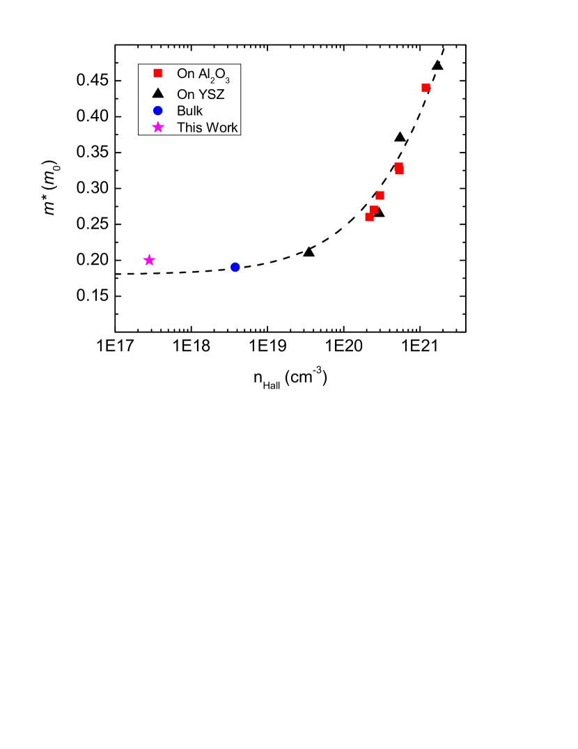
The free electron parameters were characterized via optical Hall effect measurements and compared to electrical Hall effect results. Data are shown in Fig. 11. We note that for analysis of the optical Hall effect data only one more parameter is needed, . The other two parameters, and , are already determined during the phonon mode analysis step by matching the zero field ellipsometry parameters to the best-model dielectric function. As discussed previously,Schubert et al. (2016) the optical Hall effect signatures are proportional to , and hence, combining zero field measurements with optical Hall effect measurements provides the third parameter from experiment. This then leads to determination of , and . Here we find cm-3 in excellent agreement with the electrical Hall effect density of ) cm-3. These values are also in agreement with those reported by Galazka on similar samples in 2014.Galazka, Uecker, and Fornari (2014) Due to this relatively low carrier density, the optical Hall effect data signatures are markedly small. Nonetheless, our best-match model provides a consistent fit. We also obtain the effective mass = (0.208 0.006) which is very similar to the zero density value, m0 reported by Feneberg et al.Feneberg et al. (2016) This value was obtained from matching a nonparabolic band approximation model for the effective mass parameter to a set of samples from which effective mass and free electron density parameters were determined. This data set and best-match function is reproduced in Fig. 12, where our result is included. The effective mass measured in our work by optical Hall effect corresponds to one order of magnitude lower electron density than reached by Feneberg et al., and is thus closer to the zero density value. Within our error bar, our value matches excellently with the zero density effective mass extrapolated previously. We also find the free electron mobility, cm2/(Vs) from optical Hall effect which is slightly lower than the value of 158 cm2/(Vs) obtained from electrical Hall effect, which is also within the range reported by Galazka, Uecker, and Fornari on similar oxygen annealed samples cm2/(Vs)).Galazka, Uecker, and Fornari (2014)
IV.4 Static and high frequency dielectric constants
In order to determine the high frequency dielectric constant, we extended the spectral range for our wavelength-by-wavelength analysis far above the phonon mode range, to 3000 cm-1. At frequencies far above the phonon modes yet far enough below the onset of excitonic and band-to-band transitions so that dispersion introduced by the latter is negligible, a good approximation for can be found. Our analysis resulted in 4.05 0.05. This is in good agreement with our DFT predicted value (4.128) as well as the value previously reported by Feneberg et al. (4.08).Feneberg et al. (2016) Using the LST relationship, the static dielectric constant, , can then be calculated since we have determined the complete set of phonon modes. With the values listed in Table 2 we obtain here 10.55 0.07. This value is in agreement with our DFT value of 10.74. We further conducted ellipsometry measurements at THz frequencies in order to directly evaluate the static dielectric permittivity parameters. While the free carrier concentration is small (the smallest for which effective mass parameters have been reported so far), due to the rather thick sample, our sample is opaque in the THz range. Hence, THz measurements can only be made in reflection and no substrate interferences can be detected. Such Fabry-Perot interference fringes increase sensitivity to the quasi-static DC permittivity, as demonstrated recently for -Ga2O3.Gopalan et al. (2020) Figure 10 depicts measured and best-model calculated THz Mueller matrix data measured at 50∘ angle of incidence. The best-model calculated data were obtained without further parameter variations only using the static dielectric constant and the Drude model in Eq. 7 contributions with the parameters for , , and from optical Hall effect as discussed above. The very good agreement between measured and model-calculated THz Mueller matrix data is indicative of the correctness of the static DC permittivity for In2O3, which has not been determined from experiment at DC or quasi-static frequencies previously.
V Conclusions
By using a combined approach of spectroscopic ellipsometry, DFT calculations, and optical Hall effect measurements we are able to provide a thorough investigation of the electrical and optical phonon mode properties of In2O3. All sixteen TO-LO pairs have been identified and their respective broadening parameters quantified. These values find excellent agreement with the limited sets of phonon mode information previously reported, and we introduce phonons in the far-infrared spectrum not detected thus far. Also our measured phonon modes are in excellent agreement with the results of our DFT calculations. Furthermore, by means of optical Hall effect measurements, we determine the effective electron mass at the lowest yet detected free electron density, which is in excellent agreement with the zero density effective electron mass in In2O3 predicted previously from extrapolation.
VI Acknowledgments
This work was supported in part by the National Science Foundation (NSF) under award NSF DMR 1755479, NSF DMR 1808715, by the Nebraska Materials Research Science and Engineering Center award DMR 1420645, in the framework of GraFOx, a Leibniz-Science Campus partially funded by the Leibniz Association - Germany, by Air Force Office of Scientific Research under awards FA9550-18-1-0360 and FA9550-19-S-0003, by the Swedish Research Council VR award No. 2016-00889, the Swedish Foundation for Strategic Research Grant Nos. RIF14-055 and EM16-0024, by the Swedish Governmental Agency for Innovation Systems VINNOVA under the Competence Center Program Grant No. 2016–05190, by the Knut and Alice Wallenbergs Foundation supported grant ’Wide-bandgap semiconductors for next generation quantum components’, by the Swedish Government Strategic Research Area in Materials Science on Functional Materials at Linköping University, and Faculty Grant SFO Mat LiU No. 2009-00971. Mathias Schubert acknowledges the University of Nebraska Foundation and the J. A. Woollam Foundation for financial support.
The data that support the findings of this study are available from the corresponding author upon reasonable request.
References
- King et al. (2009) P. D. C. King, T. D. Veal, F. Fuchs, C. Y. Wang, D. J. Payne, A. Bourlange, H. Zhang, G. R. Bell, V. Cimalla, O. Ambacher, R. G. Egdell, F. Bechstedt, and C. F. McConville, Phys. Rev. B 79, 205211 (2009).
- Bel Hadj Tahar et al. (1998) R. Bel Hadj Tahar, T. Ban, Y. Ohya, and Y. Takahashi, Journal of Applied Physics 83, 2631 (1998), https://doi.org/10.1063/1.367025 .
- Shigesato, Takaki, and Haranoh (1992) Y. Shigesato, S. Takaki, and T. Haranoh, Journal of Applied Physics 71, 3356 (1992), https://doi.org/10.1063/1.350931 .
- Bierwagen and Speck (2014) O. Bierwagen and J. S. Speck, physica status solidi (a) 211, 48 (2014), https://onlinelibrary.wiley.com/doi/pdf/10.1002/pssa.201330224 .
- Minami (2005) T. Minami, Semiconductor Science and Technology 20, S35 (2005).
- Lungenschmied et al. (2007) C. Lungenschmied, G. Dennler, H. Neugebauer, S. N. Sariciftci, M. Glatthaar, T. Meyer, and A. Meyer, Solar Energy Materials and Solar Cells 91, 379 (2007), selected Papers from the European Conference on Hybrid and Organic Solar Cells – ECHOS ’06.
- Diniz (2011) A. S. A. C. Diniz, Renewable Energy 36, 1153 (2011).
- Kim et al. (2009) S. I. Kim, S. H. Cho, S. R. Choi, M. C. Oh, J. H. Jang, and P. K. Song, Thin Solid Films 517, 4061 (2009), the proceedings of the 1st International Conference on Microelectronics and Plasma Technology (ICMAP 2008).
- Bartic et al. (2007) M. Bartic, C.-I. Baban, H. Suzuki, M. Ogita, and M. Isai, Journal of the American Ceramic Society 90, 2879 (2007), https://ceramics.onlinelibrary.wiley.com/doi/pdf/10.1111/j.1551-2916.2007.01842.x .
- Tischner et al. (2008) A. Tischner, T. Maier, C. Stepper, and A. Köck, Sensors and Actuators B: Chemical 134, 796 (2008).
- Kannan et al. (2010) S. Kannan, H. Steinebach, L. Rieth, and F. Solzbacher, Sensors and Actuators B: Chemical 148, 126 (2010).
- Nguyen et al. (2004) P. Nguyen, H. T. Ng, T. Yamada, M. K. Smith, J. Li, J. Han, and M. Meyyappan, Nano Letters 4, 651 (2004), https://doi.org/10.1021/nl0498536 .
- Nayak et al. (2013) P. K. Nayak, M. N. Hedhili, D. Cha, and H. N. Alshareef, Applied Physics Letters 103, 033518 (2013), https://doi.org/10.1063/1.4816060 .
- Han, Herman, and Chang (2011) S.-Y. Han, G. S. Herman, and C.-h. Chang, Journal of the American Chemical Society 133, 5166 (2011), pMID: 21417268, https://doi.org/10.1021/ja104864j .
- Kim et al. (2016) Y. G. Kim, T. Kim, C. Avis, S. Lee, and J. Jang, IEEE Transactions on Electron Devices 63, 1078 (2016).
- Sheu et al. (1998) J. K. Sheu, Y. K. Su, G. C. Chi, M. J. Jou, and C. M. Chang, Applied Physics Letters 72, 3317 (1998), https://doi.org/10.1063/1.121636 .
- Zhang et al. (2015) J. Zhang, Y. Li, B. Zhang, H. Wang, Q. Xin, and A. Song, Nature communications 6, 7561 (2015).
- Wei et al. (2010) Z. P. Wei, D. L. Guo, B. Liu, R. Chen, L. M. Wong, W. F. Yang, S. J. Wang, H. D. Sun, and T. Wu, Applied Physics Letters 96, 031902 (2010), https://doi.org/10.1063/1.3284654 .
- Gao et al. (2011) J. Gao, R. Chen, D. H. Li, L. Jiang, J. C. Ye, X. C. Ma, X. D. Chen, Q. H. Xiong, H. D. Sun, and T. Wu, Nanotechnology 22, 195706 (2011).
- Ouacha, Kleineberg, and Albrithen (2017) H. Ouacha, U. Kleineberg, and H. Albrithen, Journal of Physics D: Applied Physics 50, 455102 (2017).
- Chen, Tien, and Liao (2011) L.-C. Chen, C.-H. Tien, and W.-C. Liao, Journal of Physics D: Applied Physics 44, 165101 (2011).
- Nagata (2019) T. Nagata, in Single Crystals of Electronic Materials, Woodhead Publishing Series in Electronic and Optical Materials, edited by R. Fornari (Woodhead Publishing, 2019) pp. 523 – 546.
- Bierwagen (2015) O. Bierwagen, Semiconductor Science and Technology 30, 024001 (2015).
- Yang et al. (2008) F. Yang, J. Ma, X. Feng, and L. Kong, Journal of Crystal Growth 310, 4054 (2008).
- Karim, Feng, and Zhao (2018) M. R. Karim, Z. Feng, and H. Zhao, Crystal Growth & Design 18, 4495 (2018), https://doi.org/10.1021/acs.cgd.8b00483 .
- Galazka et al. (2013a) Z. Galazka, R. Uecker, K. Irmscher, D. Schulz, D. Klimm, M. Albrecht, M. Pietsch, S. Ganschow, A. Kwasniewski, and R. Fornari, Journal of Crystal Growth 362, 349 (2013a).
- Sadofev et al. (2012) S. Sadofev, Y. Cho, O. Brandt, M. Ramsteiner, R. Calarco, H. Riechert, S. C. Erwin, Z. Galazka, M. Korytov, M. Albrecht, R. Uecker, and R. Fornari, Applied Physics Letters 101, 172102 (2012), https://doi.org/10.1063/1.4761985 .
- Liu et al. (2019) L. Liu, S. Chen, X. Liang, and Y. Pei, Advanced Electronic Materials 5, 1900550 (2019), https://onlinelibrary.wiley.com/doi/pdf/10.1002/aelm.201900550 .
- Feneberg et al. (2016) M. Feneberg, J. Nixdorf, C. Lidig, R. Goldhahn, Z. Galazka, O. Bierwagen, and J. S. Speck, Phys. Rev. B 93, 045203 (2016).
- De Wit, Van Der Bom, and De Groot (1978) J. De Wit, J. Van Der Bom, and J. De Groot, Journal of Solid State Chemistry 25, 101 (1978).
- Preissler et al. (2013) N. Preissler, O. Bierwagen, A. T. Ramu, and J. S. Speck, Phys. Rev. B 88, 085305 (2013).
- Weiher (1962) R. L. Weiher, Journal of Applied Physics 33, 2834 (1962), https://doi.org/10.1063/1.1702560 .
- Scherer et al. (2012) V. Scherer, C. Janowitz, A. Krapf, H. Dwelk, D. Braun, and R. Manzke, Applied Physics Letters 100, 212108 (2012), https://doi.org/10.1063/1.4719665 .
- Zhang et al. (2011) K. H. L. Zhang, V. K. Lazarov, T. D. Veal, F. E. Oropeza, C. F. McConville, R. G. Egdell, and A. Walsh, Journal of Physics: Condensed Matter 23, 334211 (2011).
- Peelaers, Kioupakis, and Van de Walle (2019) H. Peelaers, E. Kioupakis, and C. G. Van de Walle, Applied Physics Letters 115, 082105 (2019), https://doi.org/10.1063/1.5109569 .
- Karazhanov et al. (2007) S. Z. Karazhanov, P. Ravindran, P. Vajeeston, A. Ulyashin, T. G. Finstad, and H. Fjellvåg, Phys. Rev. B 76, 075129 (2007).
- Fuchs and Bechstedt (2008) F. Fuchs and F. Bechstedt, Phys. Rev. B 77, 155107 (2008).
- Odaka et al. (1997) H. Odaka, S. Iwata, N. Taga, S. Ohnishi, Y. Kaneta, and Y. Shigesato, Japanese Journal of Applied Physics 36, 5551 (1997).
- Brewer and Franzen (2004) S. H. Brewer and S. Franzen, Chemical Physics 300, 285 (2004).
- Hofmann et al. (2008) T. Hofmann, V. Darakchieva, B. Monemar, H. Lu, W. Schaff, and M. Schubert, J. Electron. Mater. 37, 611 (2008).
- Kasic et al. (2000) A. Kasic, M. Schubert, S. Einfeldt, D. Hommel, and T. E. Tiwald, Phys. Rev. B 62, 7365 (2000).
- Galazka et al. (2013b) Z. Galazka, K. Irmscher, M. Pietsch, T. Schulz, R. Uecker, D. Klimm, and R. Fornari, CrystEngComm 15, 2220 (2013b).
- Galazka, Uecker, and Fornari (2014) Z. Galazka, R. Uecker, and R. Fornari, Journal of Crystal Growth 388, 61 (2014).
- Darakchieva et al. (2009) V. Darakchieva, T. Hofmann, M. Schubert, B. Sernelius, B. Monemar, P. Persson, F. Giuliani, E. Alves, H. Lu, and W. Schaff, Applied Physics Letters 94, 022109 (2009).
- Nagata et al. (2016) T. Nagata, O. Bierwagen, Z. Galazka, M. Imura, S. Ueda, H. Yoshikawa, Y. Yamashita, and T. Chikyow, Applied Physics Express 10, 011102 (2016).
- Nagata et al. (2019) T. Nagata, O. Bierwagen, Z. Galazka, M. Imura, S. Ueda, Y. Yamashita, and T. Chikyow, Japanese Journal of Applied Physics 58, SDDG06 (2019).
- Walsh (2011) A. Walsh, Applied Physics Letters 98, 261910 (2011), https://doi.org/10.1063/1.3604811 .
- Scherer et al. (2016) V. Scherer, C. Janowitz, Z. Galazka, M. Nazarzadehmoafi, and R. Manzke, EPL (Europhysics Letters) 113, 26003 (2016).
- White and Keramidas (1972) W. B. White and V. G. Keramidas, Spectrochimica Acta Part A: Molecular Spectroscopy 28, 501 (1972).
- Hamberg and Granqvist (1986) I. Hamberg and C. G. Granqvist, Journal of Applied Physics 60, R123–R160 (1986).
- Sobotta et al. (1990) H. Sobotta, H. Neumann, G. Kühn, and V. Riede, Crystal Research and Technology 25, 61 (1990), https://onlinelibrary.wiley.com/doi/pdf/10.1002/crat.2170250112 .
- Garcia-Domene et al. (2012) B. Garcia-Domene, H. M. Ortiz, O. Gomis, J. A. Sans, F. J. Manjón, A. Muñoz, P. Rodríguez-Hernández, S. N. Achary, D. Errandonea, D. Martínez-García, A. H. Romero, A. Singhal, and A. K. Tyagi, Journal of Applied Physics 112, 123511 (2012), https://doi.org/10.1063/1.4769747 .
- Kranert, Schmidt-Grund, and Grundmann (2014) C. Kranert, R. Schmidt-Grund, and M. Grundmann, physica status solidi (RRL) – Rapid Research Letters 8, 554 (2014), https://onlinelibrary.wiley.com/doi/pdf/10.1002/pssr.201409004 .
- Fiedler et al. (2019) A. Fiedler, R. Schewski, Z. Galazka, and K. Irmscher, ECS Journal of Solid State Science and Technology 8, Q3083 (2019).
- Walsh et al. (2009) A. Walsh, C. R. A. Catlow, A. A. Sokol, and S. M. Woodley, Chemistry of Materials 21, 4962 (2009), https://doi.org/10.1021/cm902280z .
- Lyddane, Sachs, and Teller (1941) R. H. Lyddane, R. Sachs, and E. Teller, Phys. Rev. 59, 613 (1941).
- Giannozzi et al. (2009) P. Giannozzi, S. Baroni, N. Bonini, M. Calandra, R. Car, C. Cavazzoni, D. Ceresoli, G. L. Chiarotti, M. Cococcioni, I. Dabo, A. D. Corso, S. de Gironcoli, S. Fabris, G. Fratesi, R. Gebauer, U. Gerstmann, C. Gougoussis, A. Kokalj, M. Lazzeri, L. Martin-Samos, N. Marzari, F. Mauri, R. Mazzarello, S. Paolini, A. Pasquarello, L. Paulatto, C. Sbraccia, S. Scandolo, G. Sclauzero, A. P. Seitsonen, A. Smogunov, P. Umari, and R. M. Wentzcovitch, J. Phys.: Cond. Mat. 21, 395502 (2009).
- Perdew and Wang (1992) J. P. Perdew and Y. Wang, Phys. Rev. B 45, 13244 (1992).
- Perdew and Wang (2018) J. P. Perdew and Y. Wang, Phys. Rev. B 98, 079904 (2018).
- van Setten et al. (2018) M. J. van Setten, M. Giantomassi, E. Bousquet, M. J. Verstraete, D. R. Hamann, X. Gonze, and G. M. Rignanese, Comput. Phys. Commun. 226, 39 (2018), 1710.10138 .
- Jain et al. (2013) A. Jain, S. P. Ong, G. Hautier, W. Chen, W. D. Richards, S. Dacek, S. Cholia, D. Gunter, D. Skinner, G. Ceder, and K. A. Persson, APL Mat. 1, 011002 (2013).
- (62) T. M. Project, .
- Monkhorst and Pack (1976) H. J. Monkhorst and J. D. Pack, Phys. Rev. B 13, 5188 (1976).
- Baroni et al. (2001) S. Baroni, S. de Gironcoli, A. D. Corso, S. Baroni, S. de Gironcoli, and P. Giannozzi, Rev. Mod. Phys. 73, 515 (2001).
- Kokalj (1999) A. Kokalj, J. Mol. Graph. Model. 17, 176 (1999).
- Gervais and Piriou (1974) F. Gervais and B. Piriou, J. Phys. C: Solid State Physics 7, 2374 (1974).
- Schubert (2004) M. Schubert, Infrared Ellipsometry on Semiconductor Layer Structures: Phonons, Plasmons and Polaritons, Springer Tracts in Modern Physics, Vol. 209 (Springer, Berlin, 2004).
- Schubert et al. (2016) M. Schubert, P. Kuehne, V. Darakchieva, and T. Hofmann, J. Opt. Soc. Am. A 33, 1553 (2016).
- Fujiwara (2007) H. Fujiwara, Spectroscopic Ellipsometry (John Wiley & Sons, New York, 2007).
- Kühne et al. (2014) P. Kühne, C. M. Herzinger, M. Schubert, J. A. Woollam, and T. Hofmann, Rev. Sci. Instrum. 85, 071301 (2014).
- Gopalan et al. (2020) P. Gopalan, S. Knight, A. Chanana, M. Stokey, P. Ranga, M. A. Scarpulla, S. Krishnamoorthy, V. Darakchieva, Z. Galazka, K. Irmscher, A. Fiedler, S. Blair, M. Schubert, and B. Sensale-Rodriguez, Applied Physics Letters 117, 252103 (2020), https://doi.org/10.1063/5.0031464 .