Thickness Dependence of Magneto-transport Properties in Tungsten Ditelluride
Abstract
We investigate the electronic structure of tungsten ditelluride (WTe2) flakes with different thicknesses in magneto-transport studies. The temperature-dependent resistance and magnetoresistance (MR) measurements both confirm the breaking of carrier balance induced by thickness reduction, which suppresses the ‘turn-on’ behavior and large positive MR. The Shubnikov-de-Haas oscillation studies further confirm the thickness-dependent change of electronic structure of WTe2 and reveal a possible temperature-sensitive electronic structure change. Finally, we report the thickness-dependent anisotropy of Fermi surface, which reveals that multi-layer WTe2 is an electronic 3D material and the anisotropy decreases as thickness decreases.
I Introduction
Tungsten ditelluride (WTe2), a layered transition metal dichalcogenide (TMD) material, has attracted a great deal of interests due to its unique electronic transport properties since the discovery of the non-saturating positive large magnetoresistance (MR) in bulk Ali et al. (2014). It is widely believed that the extraordinary MR comes from the nearly perfect balance between electron and hole concentrations Ali et al. (2014); Alekseev et al. (2015); Pletikosić et al. (2014); Thoutam et al. (2015); Wu et al. (2015); Dai et al. (2015); Luo et al. (2015). Many other peculiar electronic properties have also been observed in WTe2 in transport measurements, such as ‘turn-on’ behavior Ali et al. (2014); Wang et al. (2015a); Woods et al. (2017); Ali et al. (2015), multi-Fermi pockets revealed by Shubnikov-de-Haas (SdH) oscillations Cai et al. (2015); Zhu et al. (2015); Xiang et al. (2018), surprisingly small Fermi surface anisotropy Thoutam et al. (2015), ferroelectric property Fei et al. (2018); Sharma et al. (2019); Liu et al. (2019); Yang, Wu, and Li (2018), superconductivity Fatemi et al. (2018a); Pan et al. (2015); Kononov et al. (2021), etc. WTe2 is also a topological material. In the bulk form, WTe2 has been predicted Soluyanov et al. (2015) and observed Li et al. (2017) to be a type-II Weyl semimetal. In the monolayer form, WTe2 is a quantum spin Hall insulator Wu et al. (2018); Qian et al. (2014) at low carrier density (n). However, it is still unclear how the topological property and the electronic structure evolve by reducing the crystal thickness.
Here we investigate the evolution of electronic structure in WTe2 flakes with different thicknesses by performing temperature dependent resistance (-) measurements, MR measurements, SdH oscillation studies and angle-dependent MR measurements. Experiments show that the imbalance of carrier densities caused by thickness reduction plays an important role in the suppression of the ‘turn-on’ behavior and the large positive MR, while the non-saturating characteristic was hardly affected. We further confirm that the multi-layer WTe2 is also an electronic 3D material like bulk crystal and the anisotropy reduces as thickness decreases.
II Experiment
The WTe2 flakes with different thicknesses were obtained by mechanical exfoliation of bulk WTe2 crystals synthesized by chemical vapor transport Woods et al. (2017). Six exfoliated flakes characterized in this paper can be classified into three groups. The first group contains two thick samples (denoted as ‘sample 1’ and ‘sample 2’ hereafter) with thickness around 150 nm, the second group contains three thin flakes with thickness around 20 nm (denoted as ‘sample 3’ through ‘sample 5’ hereafter), and the third group contains one ultra-thin flake with thickness at 5 nm (‘sample 6’), whose transport properties have been reported elsewhere Zhang et al. (2020). In this paper, we will focus on the first two groups. The thick flakes are directly transferred onto silicon substrates with 285 nm-thick SiO2 coating on surface. The thin flakes was encapsulated between two pieces of hexagonal boron nitride (hBN) thin flakes which were about 10 nm thick and transferred onto the substrates by dry transfer technique Castellanos-Gomez et al. (2014). Thin WTe2 flakes get oxidized easily upon exposure to air Fatemi et al. (2018b); Wang et al. (2015b). Hence the hBN flakes are necessary here to protect the thin samples from air-induced degradation. In addition, hBN flakes provide a cleaner interface for WTe2. For the thick samples, photo-lithography was used to make the patterns. For the thin samples, electron-beam lithography was used to make patterns. The Ohmic contacts were deposited by electron-beam evaporation of Pd/Au (10 nm/200 nm for thick samples, 10 nm/40 nm for thin samples) followed by a lift-off process. Transport measurements down to 0.02 K were carried out in an Oxford dilution refrigerator. Both the longitudinal resistance and Hall resistance were measured simultaneously by using standard low frequency lock-in techniques.
III - characteristics and ‘Turn-on’ behavior
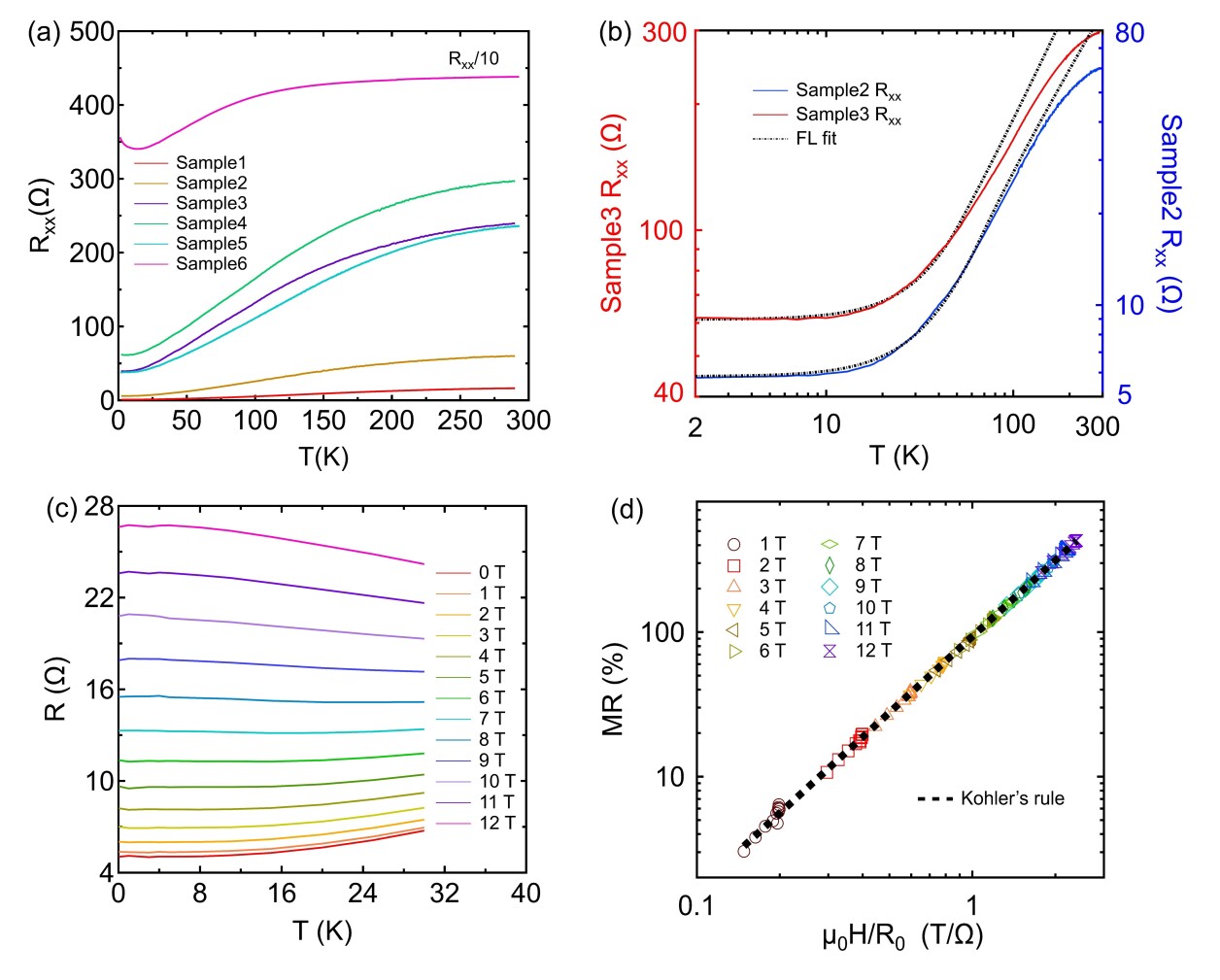
Except in the ultra-thin sample, the temperature-dependent longitudinal resistances (-) in all other five devices (samples 1-5) with different thicknesses show metallic properties across the full experiment temperature range, as shown in FIG. 1(a). The ultra-thin sample (sample 6), however, shows an insulating temperature dependence at low temperature region and it is more than 10 times resistive than all other samples. All samples in the same group show similar behavior. Thus, we pick up sample 2 and sample 3 as representatives for the thick and thin groups, respectively. In FIG. 1(b), the - curves for sample 2 and sample 3 are plotted in log-log scale and Fermi liquid fits, , applied at low temperatures are also shown as the black dashed lines for both samples. Here represents the resistance at 0 T magnetic field and are two fitting parameters. We found that the maximum applicable of the Fermi liquid fit decreased from K in sample 2 to K in sample 3 with decreasing thickness. Comparing with the case in bulk ( K) Wang et al. (2015a), the trend shows consistency that the applicable range decreases with thickness decreasing.
We further investigated the - curves at various magnetic fields up to 12 T. We unambiguously observed the ‘turn-on’ behavior in sample 2, as shown in FIG. 1(c). The - curves gradually change from metallic to insulating with magnetic field increasing from 0 T to 12 T. The critical field is around 7 T, which is much larger than the one reported in bulk (below 2 T) Ali et al. (2014); Wang et al. (2015a); Woods et al. (2017). Due to the fact that the ‘turn-on’ behavior only occurs in the Fermi liquid state Wang et al. (2015a); Khveshchenko (2001), we assume that the larger in our case is caused by the shift of the Fermi liquid state to a lower temperature region due to the thickness decreasing. Our assumption can be supported by a comparison measurement in sample 3. In sample 3, the ‘turn-on’ behavior can’t be observed up to 12 T. In a higher field, SdH oscillations emerge and disguise the ‘turn-on’ behavior. That means a magnetic field larger than 12 T is required to manifest the ‘turn-on’ behavior with the Fermi liquid state further moving to a lower temperature region (below 40 K).
In order to investigate the origin of the ‘turn-on’ behavior, we applied Kohler’s rule:
| (1) |
in which is the resistance of - curve at zero magnetic field and are the constant fitting parameters. Here MR is defined as MR=. We found that the R-T curves in FIG. 1(c) can be scaled into one curve. Specifically, the Kohler’s rule fitting gave the parameter . Comparing with the case in bulk () Wang et al. (2015a), decreased and deviated further from the perfect carrier compensation of Sondheimer and Wilson (1947); Chan et al. (2014); Murzin et al. (1998). The scaling behavior obtained by Kohler’s rule confirmed that the - curves at different magnetic fields have the same temperature dependence, although it looks like the curve at higher field shows larger MR effect. This is quite different from the case of a magnetic field-induced metal-insulator transition, which requires a larger increasing rate at a higher magnetic field due to gap opening Khveshchenko (2001); Kopelevich et al. (2006). In addition, our results show that the ‘turn-on’ behavior takes its origin from carrier compensation. The nearly broken carrier compensation in sample 3 () makes the ‘turn-on’ behavior almost invisible even at 12 T.
IV Two-band model fittings
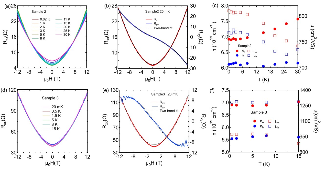
To further confirm whether perfect carrier compensation is related to the ‘turn-on’ behavior or not, we performed MR measurements on both samples. The MR curves of both samples at different temperatures are shown in FIG. 2(a) and 2(d). We found that the MR curves in sample 2 crossed at two points located at 7 T and -7 T, respectively. This is consistent with the of the ‘turn-on’ behavior. However, it’s almost impossible to identify such two crossing points in sample 3 since the MR curves at different temperatures are fully overlapped in large magnetic field region. This is also consistent with the fact that we didn’t observe obvious ‘turn-on’ behavior in sample 3.
Quasi-quadratic positive MR can be seen in both samples, which has been attributed to the perfectly balanced electron and hole densities Pletikosić et al. (2014); Woods et al. (2017); Thoutam et al. (2015); Wu et al. (2015); Dai et al. (2015); Luo et al. (2015). Comparing with the results in bulk Ali et al. (2014), which recorded MR as high as 13,000,000 , the highest MR in our samples only showed 1,200 due to reduction in thickness. The MR in both samples is notably suppressed, which indicates an imperfect balance between carrier densities and more impact from defects. But there’s still no observed trend towards saturation of MR in the samples. In order to examine the balance between carrier densities further, we additionally performed Hall measurements. Combined with MRs, we could extract the carrier densities and mobilities using the two-band model Ashcroft, Mermin et al. (1976); Rullier-Albenque et al. (2009, 2010):
| (2) | |||||
| (3) |
in which are the conductance contributions from electron and hole, respectively. are the Hall coefficients for electron-dominant and hole-dominant Hall effect. and are carrier densities and mobilities, respectively. The fitting results and the extracted carrier densities and mobilities are shown in FIG. 2.
The two-band model was perfectly applicable to our MR and Hall measurements for sample 2, while there’s a little mismatch in the low field region of MR for sample 3 (Fig. 2(e)). The low-field mismatch might come from the disorder-induced quantum interference effect Zhang et al. (2020); Lu, Shi, and Shen (2011); Hikami, Larkin, and Nagaoka (1980); Lu and Shen (2014), which is more pronounced in ultra-thin sample where weal localization and weak anti-localization effects are stronger. However, this small mismatch doesn’t have decisive influence on the extraction of carrier densities and mobilities. In sample 2, we found that the hole density was almost unchanged with temperature while the electron density gradually increases with temperature increasing (Fig. 2(c)). Such a trend is consistent with other transport and ARPES studies Pletikosić et al. (2014); Thoutam et al. (2015); Wu et al. (2015); Dai et al. (2015); Luo et al. (2015). However, the electron and hole densities are not completely equal at low temperature in our samples. The charge carrier density ratio, , is about 1.15 in sample 2 and becomes even larger in sample 3, which is 1.26. It indicates that the perfect balance between electron and hole carrier densities will be gradually broken as the thickness decreases. Furthermore, such a growing charge imbalance will cause the MR to be continuously suppressed and will also cause the ‘turn-on’ behavior to become insignificant and eventually disappear. However, it seems that the MR can still maintain the non-saturating characteristic at large field up to 12 T, no matter how much the MR is suppressed. While the MR in some imbalanced-carrier systems tends to saturate eventually at high magnetic fields Yang et al. (1999); Kopelevich et al. (2003), it is not observed in our experiments. This could be attributed to the fact the either the magnetic field used in our experiment is not large enough or the origin of the non-saturating characteristic is not the perfect balance of electron and hole compensation. Actually a linear non-saturating MR has been observed in some Dirac semimetals Liang et al. (2015); Liu et al. (2014); Shekhar et al. (2015); Ghimire et al. (2015); Xu et al. (2015), which is believed to take the origin of the lifting of a remarkable protection mechanism induced by time reversal symmetry that strongly suppresses backscatterings at zero magnetic fields. Similar linear MR curves have been observed in disordered WTe2 flakes Zhang et al. (2020); Liu et al. (2016). Possible link between the non-saturating MR in WTe2 and such a mechanism also deserves further investigation.
It is worth mentioning that both the electron and hole mobilities in sample 2 increased with decreasing temperature, which might be due to the suppression of phonon scattering at lower temperatures. In sample 3, the electron and hole mobilities were larger than those in sample 2 and remained largely unchanged with temperature. This may indicate the mobility enhancement brought about by the encapsulating hBN flakes, which eliminate the interface scattering.
V Shubnikov de Haas oscillations
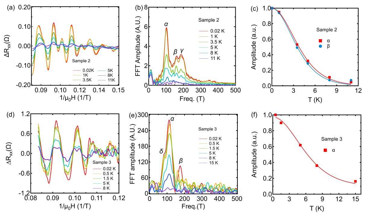
SdH oscillations can be obviously seen at low temperature MR traces (FIG. 2(a) and 2(d)) due to the high carrier mobility and the strong suppression of phonon scattering at low temperatures. The SdH oscillations were extracted from the MR curves by removing the quasi-quadratic backgrounds. The extracted oscillations at different temperatures are shown in FIG. 3(a) and 3(d) for sample 2 and sample 3, respectively. FIG. 3(b) and 3(e) shows the corresponding Fourier transformation (FT) analysis. There were three obvious peaks observed in both sample 2 and sample 3. In sample 2, the three peaks are located at 102 T (), 161 T () and 187 T (). These peak locations almost stay unchanged with temperature. In sample 3, the two peaks located at 84 T and 113 T, and the third peak located at 176 T at 0.02 K and re-located to 162 T above 0.02 K. According to the similarity of locations in sample 2, we assigned a new symbol to the first peak, to the second peak and to the third peak.
According to the Onsager relation , where is the oscillation frequency, is the flux quantum, the cross-sectional area of each Fermi pocket can be obtained: Å-2 for , , pockets in sample 2, respectively. And (at 0.02 K) and (above 0.02 K) Å-2 for , and pockets in sample 3, respectively. It is inaccurate to identify the carrier types of the Fermi pockets based on both the size of each Fermi pocket and the carrier densities obtained from the two-band model fittings, but we can conclude that the electronic structure changes dramatically with thickness, since one pocket () disappears while a new one () appears in sample 3. In addition, the shift of the pocket with temperature in sample 3 reveals a temperature-sensitive electronic structure of multi-layer WTe2. Besides the Fermi pocket topology, a temperature-induced spin splitting can be explicitly observed in sample 3, as shown in FIG. 3(d). The oscillation peaks double-split with increasing temperature, which is contrary to the common belief that the spin splitting only occurs at low temperature and high magnetic field. What happened here might be due to the breaking of spin-orbit coupling (SOC) with increasing temperature. It has been proved that SOC can be strongly suppressed by temperature in WTe2 Zhang et al. (2020). At low temperature, the SOC is strong so that the applied magnetic field is not sufficient to support an observable Zeeman splitting. At higher temperature, the missing or non-dominant SOC enables the appearance of the Paschen–Back effect at moderate magnetic field Paschen and Back (1921); Kapitza, Strelkov, and Laurman (1938); Abe et al. (2019).
The Lifshitz-Kosevich (LK) formula is commonly used to analyze the SdH oscillations Shoenberg (2009). The damping factor shown below in the LK formula is used to describe the temperature dependence of the oscillation amplitude,
| (4) |
in which is the Boltzmann constant and is the effective mass. FIG. 3(c) and 3(f) show the fitting results for the Fermi pockets in sample 2 and sample 3, respectively. Since the amplitude of the peak in sample 2 and peak in sample 3 cannot be reliably extracted above 3.5 K and the peak in sample 3 shifts location, we excluded them from the fitting analysis. The effective mass obtained from fittings are: and for sample 2, and for sample 3, where is the free electron mass. We notice that sample 2 shows comparable results with those in bulk, whereas for sample 3, the effective mass is slightly lighter. This might result from the enhanced carrier mobilities due to the encapsulated structure Cai et al. (2015); Xiang et al. (2015, 2018).
VI Fermi surface anisotropy
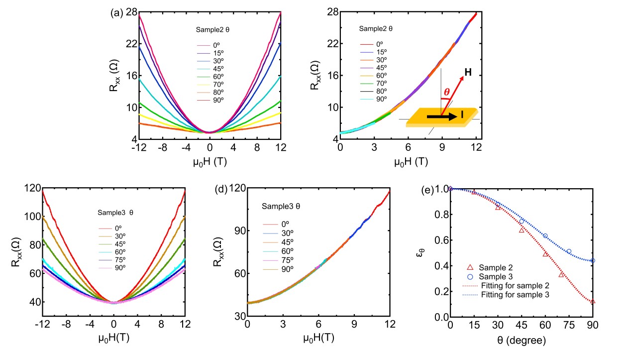
We further measured the angle-dependent MR curves, as shown in FIG. 4(a) and 4(c) for sample 2 and sample 3, respectively. is the angle between the direction of the magnetic field and the normal direction of the sample, as shown in the inset of FIG. 4(b). It is observed that the non-saturating positive MR is strongly suppressed when the magnetic field is parallel to the sample surface. Magnetoresistance oscillation study shows that the peaks in the FT spectrum shift with angle, which indicates the Fermi surface anisotropy between the in-plane and out-of-plane directions. So we further investigated the anisotropy of the Fermi surface through the scaling behavior of MR curves. The scaling behavior Blatter, Geshkenbein, and Larkin (1992); Noto and Tsuzuku (1975); Thoutam et al. (2015) can be expressed as:
| (5) |
with the scaling factor . All the MR curves can be scaled into a single curve as shown in FIG. 4(b) and 4(d), respectively, for both samples. Since the sample resistance is directly related to the effective mass by , where is the relaxation time, the scaling behavior of MR can describe the mass anisotropy , which is the in the equation. In addition, since manifests the energy band curvature, alone can also be used to describe the anisotropy of Fermi surface Noto and Tsuzuku (1975); Soule (1958); Soule, McClure, and Smith (1964); Thoutam et al. (2015).
The scaling factors were obtained for both samples at different angles and plotted in FIG. 4(e). By fitting the scaling factor versus angle, we got the anisotropy parameter and 2.28 in sample 2 and sample 3, respectively. Interestingly, the anisotropy we got from WTe2 is much smaller than that in graphite Noto and Tsuzuku (1975), a typical layered material. It is even more striking that the anisotropy parameter in the thick sample is larger than the one in the thin sample. That means the electrons in a thinner WTe2 can move more freely along direction than in a thick one. Such a small Fermi surface anisotropy indicates that WTe2 is actually an electronic 3D material. Unlike the isotropic electron gas, however, the 3D electron gas (3DEG) in WTe2 along the stacking direction is strongly modulated by sample thickness. When the thickness reduces to the order of nanometers, a thinner sample may suffer less interlayer scatterings along the stacking direction, thereby making the movement of electrons in this direction less constrained.
VII Conclusion
With a thorough magneto-transport study in a series of WTe2 flakes, we have observed a systematic change of electronic structure as a function of the thickness. First, we confirmed that the Kohler’s rule is applicable and responsible for the ‘turn-on’ behavior which normally occurs in Fermi liquid state, thereby ruling out the possibility of a metal-insulator transition. Second, we found that the imbalance of carrier densities took an important role on the suppression of ‘turn-on’ behavior and large positive MR, while the non-saturating characteristic was hardly affected. This might hint at some other origins for such a MR. Third, the SdH oscillation studies further shown the important role of thickness on the Fermi surface in WTe2 and perhaps a temperature-sensitive change in electronic structure. Finally, we reported a thickness-dependent Fermi surface anisotropy, which revealed that WTe2, a typical 2D Van der Waals material, is effectively an electronic 3D material and the anisotropy decreases with decreasing thickness.
Acknowledgements.
This work was supported by UT Dallas SPIRe fund (No. 2108630). Synthesis of WTe2 crystals was supported by DOE BES Award No. DE-SC0014476.References
- Ali et al. (2014) M. N. Ali, J. Xiong, S. Flynn, J. Tao, Q. D. Gibson, L. M. Schoop, T. Liang, N. Haldolaarachchige, M. Hirschberger, N. P. Ong, et al., “Large, non-saturating magnetoresistance in WTe2,” Nature 514, 205–208 (2014).
- Alekseev et al. (2015) P. Alekseev, A. Dmitriev, I. Gornyi, V. Y. Kachorovskii, B. Narozhny, M. Schütt, and M. Titov, “Magnetoresistance in two-component systems,” Physical Review Letters 114, 156601 (2015).
- Pletikosić et al. (2014) I. Pletikosić, M. N. Ali, A. Fedorov, R. J. Cava, and T. Valla, “Electronic structure basis for the extraordinary magnetoresistance in WTe2,” Physical Review Letters 113, 216601 (2014).
- Thoutam et al. (2015) L. Thoutam, Y. Wang, Z. Xiao, S. Das, A. Luican-Mayer, R. Divan, G. Crabtree, and W. Kwok, “Temperature-dependent three-dimensional anisotropy of the magnetoresistance in WTe2,” Physical Review Letters 115, 046602 (2015).
- Wu et al. (2015) Y. Wu, N. H. Jo, M. Ochi, L. Huang, D. Mou, S. L. Bud’ko, P. C. Canfield, N. Trivedi, R. Arita, and A. Kaminski, “Temperature-induced Lifshitz transition in WTe2,” Physical Review Letters 115, 166602 (2015).
- Dai et al. (2015) Y. Dai, J. Bowlan, H. Li, H. Miao, S. Wu, W. Kong, P. Richard, Y. Shi, S. Trugman, J.-X. Zhu, et al., “Ultrafast carrier dynamics in the large-magnetoresistance material WTe2,” Physical Review B 92, 161104 (2015).
- Luo et al. (2015) Y. Luo, H. Li, Y. Dai, H. Miao, Y. Shi, H. Ding, A. Taylor, D. Yarotski, R. Prasankumar, and J. Thompson, “Hall effect in the extremely large magnetoresistance semimetal WTe2,” Applied Physics Letters 107, 182411 (2015).
- Wang et al. (2015a) Y. Wang, L. Thoutam, Z. Xiao, J. Hu, S. Das, Z. Mao, J. Wei, R. Divan, A. Luican-Mayer, G. Crabtree, et al., “Origin of the turn-on temperature behavior in WTe2,” Physical Review B 92, 180402 (2015a).
- Woods et al. (2017) J. M. Woods, J. Shen, P. Kumaravadivel, Y. Pang, Y. Xie, G. A. Pan, M. Li, E. I. Altman, L. Lu, and J. J. Cha, “Suppression of magnetoresistance in thin WTe2 flakes by surface oxidation,” ACS Applied Materials & Interfaces 9, 23175–23180 (2017).
- Ali et al. (2015) M. N. Ali, L. Schoop, J. Xiong, S. Flynn, Q. Gibson, M. Hirschberger, N. P. Ong, and R. J. Cava, “Correlation of crystal quality and extreme magnetoresistance of WTe2,” EPL (Europhysics Letters) 110, 67002 (2015).
- Cai et al. (2015) P. Cai, J. Hu, L. He, J. Pan, X. Hong, Z. Zhang, J. Zhang, J. Wei, Z. Mao, and S. Li, “Drastic pressure effect on the extremely large magnetoresistance in WTe2: quantum oscillation study,” Physical Review Letters 115, 057202 (2015).
- Zhu et al. (2015) Z. Zhu, X. Lin, J. Liu, B. Fauqué, Q. Tao, C. Yang, Y. Shi, and K. Behnia, “Quantum oscillations, thermoelectric coefficients, and the fermi surface of semimetallic WTe2,” Physical Review Letters 114, 176601 (2015).
- Xiang et al. (2018) F.-X. Xiang, A. Srinivasan, Z. Du, O. Klochan, S.-X. Dou, A. R. Hamilton, and X.-L. Wang, “Thickness-dependent electronic structure in WTe2 thin films,” Physical Review B 98, 035115 (2018).
- Fei et al. (2018) Z. Fei, W. Zhao, T. A. Palomaki, B. Sun, M. K. Miller, Z. Zhao, J. Yan, X. Xu, and D. H. Cobden, “Ferroelectric switching of a two-dimensional metal,” Nature 560, 336–339 (2018).
- Sharma et al. (2019) P. Sharma, F.-X. Xiang, D.-F. Shao, D. Zhang, E. Y. Tsymbal, A. R. Hamilton, and J. Seidel, “A room-temperature ferroelectric semimetal,” Science Advances 5, eaax5080 (2019).
- Liu et al. (2019) X. Liu, Y. Yang, T. Hu, G. Zhao, C. Chen, and W. Ren, “Vertical ferroelectric switching by in-plane sliding of two-dimensional bilayer WTe2,” Nanoscale 11, 18575–18581 (2019).
- Yang, Wu, and Li (2018) Q. Yang, M. Wu, and J. Li, “Origin of two-dimensional vertical ferroelectricity in WTe2 bilayer and multilayer,” The Journal of Physical Chemistry Letters 9, 7160–7164 (2018).
- Fatemi et al. (2018a) V. Fatemi, S. Wu, Y. Cao, L. Bretheau, Q. D. Gibson, K. Watanabe, T. Taniguchi, R. J. Cava, and P. Jarillo-Herrero, “Electrically tunable low-density superconductivity in a monolayer topological insulator,” Science 362, 926–929 (2018a).
- Pan et al. (2015) X.-C. Pan, X. Chen, H. Liu, Y. Feng, Z. Wei, Y. Zhou, Z. Chi, L. Pi, F. Yen, F. Song, et al., “Pressure-driven dome-shaped superconductivity and electronic structural evolution in tungsten ditelluride,” Nature Communications 6, 1–6 (2015).
- Kononov et al. (2021) A. Kononov, M. Endres, G. Abulizi, K. Qu, J. Yan, D. G. Mandrus, K. Watanabe, T. Taniguchi, and C. Schönenberger, “Superconductivity in type-II Weyl-semimetal WTe2 induced by a normal metal contact,” Journal of Applied Physics 129, 113903 (2021).
- Soluyanov et al. (2015) A. A. Soluyanov, D. Gresch, Z. Wang, Q. Wu, M. Troyer, X. Dai, and B. A. Bernevig, “Type-II Weyl semimetals,” Nature 527, 495–498 (2015).
- Li et al. (2017) P. Li, Y. Wen, X. He, Q. Zhang, C. Xia, Z.-M. Yu, S. A. Yang, Z. Zhu, H. N. Alshareef, and X.-X. Zhang, “Evidence for topological type-II Weyl semimetal WTe2,” Nature Communications 8, 1–8 (2017).
- Wu et al. (2018) S. Wu, V. Fatemi, Q. D. Gibson, K. Watanabe, T. Taniguchi, R. J. Cava, and P. Jarillo-Herrero, “Observation of the quantum spin Hall effect up to 100 Kelvin in a monolayer crystal,” Science 359, 76–79 (2018).
- Qian et al. (2014) X. Qian, J. Liu, L. Fu, and J. Li, “Quantum spin Hall effect in two-dimensional transition metal dichalcogenides,” Science 346, 1344–1347 (2014).
- Zhang et al. (2020) X. Zhang, J. M. Woods, J. J. Cha, and X. Shi, “Crossover between weak antilocalization and weak localization in few-layer WTe2: Role of electron-electron interactions,” Physical Review B 102, 115161 (2020).
- Castellanos-Gomez et al. (2014) A. Castellanos-Gomez, M. Buscema, R. Molenaar, V. Singh, L. Janssen, H. S. Van Der Zant, and G. A. Steele, “Deterministic transfer of two-dimensional materials by all-dry viscoelastic stamping,” 2D Materials 1, 011002 (2014).
- Fatemi et al. (2018b) V. Fatemi, S. Wu, Y. Cao, L. Bretheau, Q. D. Gibson, K. Watanabe, T. Taniguchi, R. J. Cava, and P. Jarillo-Herrero, “Electrically tunable low-density superconductivity in a monolayer topological insulator,” Science 362, 926–929 (2018b).
- Wang et al. (2015b) L. Wang, I. Gutiérrez-Lezama, C. Barreteau, N. Ubrig, E. Giannini, and A. F. Morpurgo, “Tuning magnetotransport in a compensated semimetal at the atomic scale,” Nature Communications 6, 1–7 (2015b).
- Khveshchenko (2001) D. Khveshchenko, “Magnetic field-induced semimetal-insulator transition in graphite,” Physical Review Letter 87, 206401 (2001).
- Sondheimer and Wilson (1947) E. Sondheimer and A. H. Wilson, “The theory of the magneto-resistance effects in metals,” Proceedings of the Royal Society of London. Series A. Mathematical and Physical Sciences 190, 435–455 (1947).
- Chan et al. (2014) M. Chan, M. Veit, C. Dorow, Y. Ge, Y. Li, W. Tabis, Y. Tang, X. Zhao, N. Barišić, and M. Greven, “In-plane magnetoresistance obeys Kohler’s rule in the pseudogap phase of cuprate superconductors,” Physical Review Letters 113, 177005 (2014).
- Murzin et al. (1998) S. Murzin, S. Dorozhkin, G. Landwehr, and A. Gossard, “Effect of hole-hole scattering on the conductivity of the two-component 2D hole gas in GaAs/(AlGa) As heterostructures,” Journal of Experimental and Theoretical Physics Letters 67, 113–119 (1998).
- Kopelevich et al. (2006) Y. Kopelevich, J. M. Pantoja, R. Da Silva, and S. Moehlecke, “Universal magnetic-field-driven metal-insulator-metal transformations in graphite and bismuth,” Physical Review B 73, 165128 (2006).
- Ashcroft, Mermin et al. (1976) N. W. Ashcroft, N. D. Mermin, et al., Solid state physics (Holt, Rinehart and Winston, New York London, 1976).
- Rullier-Albenque et al. (2009) F. Rullier-Albenque, D. Colson, A. Forget, and H. Alloul, “Hall effect and resistivity study of the magnetic transition, carrier content, and Fermi-liquid behavior in Ba(Fe1-xCox)2As2,” Physical Review Letters 103, 057001 (2009).
- Rullier-Albenque et al. (2010) F. Rullier-Albenque, D. Colson, A. Forget, P. Thuéry, and S. Poissonnet, “Hole and electron contributions to the transport properties of Ba(Fe1-xRux)2As2 single crystals,” Physical Review B 81, 224503 (2010).
- Lu, Shi, and Shen (2011) H.-Z. Lu, J. Shi, and S.-Q. Shen, “Competition between weak localization and antilocalization in topological surface states,” Physical Review Letters 107, 076801 (2011).
- Hikami, Larkin, and Nagaoka (1980) S. Hikami, A. I. Larkin, and Y. Nagaoka, “Spin-orbit interaction and magnetoresistance in the two dimensional random system,” Progress of Theoretical Physics 63, 707–710 (1980).
- Lu and Shen (2014) H.-Z. Lu and S.-Q. Shen, “Finite-temperature conductivity and magnetoconductivity of topological insulators,” Physical Review Letters 112, 146601 (2014).
- Yang et al. (1999) F. Yang, K. Liu, K. Hong, D. Reich, P. Searson, and C. Chien, “Large magnetoresistance of electrodeposited single-crystal bismuth thin films,” Science 284, 1335–1337 (1999).
- Kopelevich et al. (2003) Y. Kopelevich, J. Torres, R. R. da Silva, F. Mrowka, H. Kempa, and P. Esquinazi, “Reentrant metallic behavior of graphite in the quantum limit,” Physical Review Letters 90, 156402 (2003).
- Liang et al. (2015) T. Liang, Q. Gibson, M. N. Ali, M. Liu, R. Cava, and N. Ong, “Ultrahigh mobility and giant magnetoresistance in the Dirac semimetal Cd3As2,” Nature Materials 14, 280–284 (2015).
- Liu et al. (2014) Z. Liu, B. Zhou, Y. Zhang, Z. Wang, H. Weng, D. Prabhakaran, S.-K. Mo, Z. Shen, Z. Fang, X. Dai, et al., “Discovery of a three-dimensional topological Dirac semimetal, Na3Bi,” Science 343, 864–867 (2014).
- Shekhar et al. (2015) C. Shekhar, A. K. Nayak, Y. Sun, M. Schmidt, M. Nicklas, I. Leermakers, U. Zeitler, Y. Skourski, J. Wosnitza, Z. Liu, et al., “Extremely large magnetoresistance and ultrahigh mobility in the topological Weyl semimetal candidate NbP,” Nature Physics 11, 645–649 (2015).
- Ghimire et al. (2015) N. J. Ghimire, Y. Luo, M. Neupane, D. Williams, E. Bauer, and F. Ronning, “Magnetotransport of single crystalline NbAs,” Journal of Physics: Condensed Matter 27, 152201 (2015).
- Xu et al. (2015) S.-Y. Xu, N. Alidoust, I. Belopolski, Z. Yuan, G. Bian, T.-R. Chang, H. Zheng, V. N. Strocov, D. S. Sanchez, G. Chang, et al., “Discovery of a Weyl fermion state with Fermi arcs in niobium arsenide,” Nature Physics 11, 748–754 (2015).
- Liu et al. (2016) W. L. Liu, M. L. Chen, X. X. Li, S. Dubey, T. Xiong, Z. M. Dai, J. Yin, W. L. Guo, J. L. Ma, Y. N. Chen, et al., “Effect of aging-induced disorder on the quantum transport properties of few-layer WTe2,” 2D Materials 4, 011011 (2016).
- Paschen and Back (1921) F. Paschen and E. Back, “Liniengruppen magnetisch vervollständigt,” Physica 1, 261–273 (1921).
- Kapitza, Strelkov, and Laurman (1938) P. L. Kapitza, P. Strelkov, and E. Laurman, “The Zeeman and Paschen-Back effects in strong magnetic fields,” Proceedings of the Royal Society of London. Series A. Mathematical and Physical Sciences 167, 1–15 (1938).
- Abe et al. (2019) M. Abe, R. Itoyama, Y. Komiyama, T. Ito, T. Mashimo, and S. Tojo, “Quantitative investigation of the Zeeman and Paschen-Back effects of the hyperfine structure during the rubidium 52S52D5/2 two-photon transition,” Physical Review A 99, 053420 (2019).
- Shoenberg (2009) D. Shoenberg, Magnetic oscillations in metals (Cambridge university press, 2009).
- Xiang et al. (2015) F.-X. Xiang, M. Veldhorst, S.-X. Dou, and X.-L. Wang, “Multiple Fermi pockets revealed by Shubnikov-de Haas oscillations in WTe2,” EPL (Europhysics Letters) 112, 37009 (2015).
- Blatter, Geshkenbein, and Larkin (1992) G. Blatter, V. B. Geshkenbein, and A. Larkin, “From isotropic to anisotropic superconductors: a scaling approach,” Physical Review Letters 68, 875 (1992).
- Noto and Tsuzuku (1975) K. Noto and T. Tsuzuku, “A simple two-band theory of galvanomagnetic effects in graphite in relation to the magnetic field azimuth,” Japanese Journal of Applied Physics 14, 46 (1975).
- Soule (1958) D. Soule, “Magnetic field dependence of the Hall effect and magnetoresistance in graphite single crystals,” Physical Review 112, 698 (1958).
- Soule, McClure, and Smith (1964) D. Soule, J. McClure, and L. Smith, “Study of the Shubnikov-de Haas effect. Determination of the Fermi surfaces in graphite,” Physical Review 134, A453 (1964).