Institut für Theoretische Physik und Astrophysik, Christian-Albrechts-Universität zu Kiel, D-24098 Kiel, Germany \alsoaffiliationHelmholtz-Zentrum für Materialien und Energie GmbH, Berlin, Germany \alsoaffiliationHelmholtz-Zentrum für Materialien und Energie GmbH, Berlin, Germany
Two-dimensional plasmonic polarons in n-doped monolayer MoS2
Abstract
We report experimental and theoretical evidence of strong electron-plasmon interaction in -doped single-layer MoS2. Angle-resolved photoemission spectroscopy (ARPES) measurements reveal the emergence of distinctive signatures of polaronic coupling in the electron spectral function. Calculations based on many-body perturbation theory illustrate that electronic coupling to two-dimensional (2D) carrier plasmons provides an exhaustive explanation of the experimental spectral features and their energies. These results constitute compelling evidence of the formation of plasmon-induced polaronic quasiparticles, suggesting that highly-doped transition-metal dichalcogenides may provide a new platform to explore strong-coupling phenomena between electrons and plasmons in 2D.
The interplay of charge confinement, reduced dielectric screening, and strong light-matter coupling in few-layer semiconducting transition-metal dichalcogenides (TMDCs) underpins a vast spectrum of emergent many-body effects, including the formation of excitons 1, 2, 3, 4, trions 5, polarons 6, 7, polaritons 8, 9, 10, 11, 12, and superconductivity 13. At variance with three-dimensional solids, TMDCs further allows for unprecedented opportunities to tailor these phenomena via cavity embedding 14, circular dichroism 15, 16, gating 13, nano-structuring 17, 12, substrate engineering 18, and doping 6.
Highly-tunable carrier densities are particularly desirable for the study of many-body interactions in TMDCs, as they may enable control of plasmons (collective excitation of the electron density) and polarons (electrons dressed by a phonon cloud) 19, 20. Polarons typically arise in semiconductors and insulators as a result of strong coupling to longitudinal-optical (LO) vibrational modes 19, 21, 20, 22. Polarons may lead to charge trapping 21, 23 and to a renormalization of the band effective masses 22. The relevance of such phenomena for the opto-electronic properties of solids, alongside with the recent discovery of polarons in the photoemission spectrum of doped oxides 19, 20 and 2D materials 6, 24, has reignited theoretical and experimental research on polaronic quasiparticles 21, 23, 22, 25, 26, 7, 27, 28.
In close analogy to phonon-induced polarons, the formation of polaronic quasiparticles may also be stimulated by the coupling to extrinsic plasmons in highly-doped semiconductors 25, leading to distinctive satellite features in angle-resolved photoemission spectroscopy (ARPES). The experimental observation of plasmonic polarons in three-dimensional solids is hindered by rather low electron-plasmon coupling strengths ( 25), and by the difficulty to achieve degenerate doping concentrations (a prerequisite for the excitation of plasmons) while simultaneously retaining crystallinity of the sample. Single-layer TMDCs circumvent this problem since highly-tunable carrier densities can be realized. In particular, some of us have recently demonstrated that the carrier population in the conduction band of monolayer MoS2 and WS2 can be tailored by stimulating the formation of chalcogen vacancies via repeated annealing cycles 29. Additionally, we show here that the 2D confinement of plasmons and charge carriers provide suitable conditions for the establishment of a strong-coupling regime, leading to the emergence of plasmonic-polaron quasiparticles.
In this manuscript, we report the observation of plasmon-induced polarons in -doped monolayer MoS2. ARPES measurements of the conduction band reveals distinctive fingerprints of bosonic satellites due to electron-boson coupling. The satellite energy, ranging between 130 and 200 meV, is much larger than the characteristic phonon energies ( meV), and depends pronouncedly on the carrier density. These characteristics are incompatible with a coupling mechanism due to LO phonons. By explicitly accounting for the effects of electronic coupling to 2D plasmons in a first-principles many-body framework, our calculations of the spectral function identify electron-plasmon interactions as the origin of the polaronic spectral features observed in experiments. These findings provide compelling evidence of the emergence of 2D plasmonic polarons in -doped monolayer MoS2, and they demonstrate the establishment of a strong-coupling regime resulting from the confinement of carriers and plasmons in 2D.
The measured samples consist of a chemical-vapor-deposition (CVD) grown fully-closed MoS2 monolayer film with azimuthal disorder on a sapphire substrate 30. Top mechanical clamping of the sample enabled electrical contact of the monolayer to ground. Sample charging during ARPES measurements was avoided upon doping of the monolayer as described thereafter. Degenerate -doping was achieved by repeated in-situ vacuum annealing cycles (with final annealing for 12 hours at 850 K), which is known to effectively -dope MoS2 monolayer 31. The Fermi-level position (corresponding to 0 eV binding energy) and the instrumental broadening were determined by fitting the Fermi edge of a gold polycrystal using a broadened Fermi-Dirac function. The estimate doping concentrations , , and cm-2 (referred to simply as , , in the following), result from the formation of sulfur vacancies either by direct desorption of sulfur atoms or by desorption of substitutional oxygen present at sulfur-vacancy sites, naturally present in CVD grown samples 32, 33. Our calculations indicate that this concentration of S vacancies leaves the band structure unchanged (Supplementary Note 5 and Fig. S4 in the Supporting Information (SI)). The photoemission measurements on and were performed in an analysis chamber (base pressure mbar) equipped with a Specs Phoibos 100 hemispherical electron analyzer and using the HeI radiation provided by monochromated helium discharge lamp (consisting of a HIS-13 lamp mounted on a VUV5046 UV-monochromator). These measurements were performed at room temperature. The overall energy resolution amounted to 117 meV (65 meV instrumental energy resolution) as determined from the Fermi edge of a polycrystalline gold sample and the angular resolution was about degrees. The ARPES measurements on were performed at 230 K using a DA30-L hemispherical analyzer with an angular resolution of ca. 0.3 ∘ and an overall resolution of 100 meV (65 meV instrumental energy resolution). The energy distribution curves were measured every two degrees by rotating the manipulator about the polar axis. Despite photoemission averaging over all azimuthal orientations as exhibited by the MoS2 grains, the low dimensionality of the system promotes the observation in the ARPES spectra of well-resolved electronic band dispersion along the high-symmetry directions -K and -M 34.
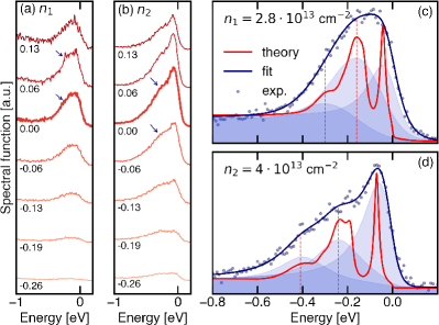
Figures 1 (a) and (b) report ARPES spectral functions of monolayer MoS2 for crystal momenta in the vicinity of the high-symmetry point K for doping concentrations and , respectively, whereas the full measured spectral function for the valence band is shown in Fig. S5 in the SI. The on-curve labels indicate the photo-electron crystal momentum , relative to the K point in units of Å-1. Energies are referenced to the Fermi level that is located 39 and 56 meV above the conduction-band minimum (CBm), respectively. At K and neighboring crystal momenta, the spectral functions are characterized by a quasiparticle peak close to the Fermi level. The peak position corresponds to the binding energy of quasi-electrons around the CBm. At binding energies larger than those of quasiparticle excitations, the spectral function for carrier concentration () exhibits a shoulder-like structure red-shifted by 130 meV (170 meV) from the quasiparticle peak and extending up to 0.6 eV below the Fermi level. These spectral features, indicated by arrows in Figs. 1 (a) and (b), become more pronounced at higher carrier densities.
A more detailed view of these spectral signatures is given in Figs. 1 (c) and (d), which report the spectral functions for and (corresponding to the thick lines in Figs. 1 (a) and (b)), whereas measurements for a third carrier concentration () are reported in Fig. S7 (see SI). For , the spectral function exhibits a satellite structure at 170 meV and a less-pronounced secondary structure at 330 meV below the quasiparticle peak. These features become more pronounced for momenta close to the K point at Å-1 (Fig. S6 in the SI). To better resolve the underlying spectral features that give rise to the satellite, in Fig. S8 we apply the prescription of Ref. 35 and de-convolute the experimental spectra by a Gaussian function to reduce the spectral broadening due to finite resolution and lifetime effects. These spectral features closely resemble the characteristic spectral fingerprints of electron-boson interaction in photoemission spectroscopy. Specifically: (i) they have non-vanishing intensity within the gap and, therefore, may not be attributed to the emission of a photo-electron; (ii) they are roughly spaced from the quasiparticle peak by multiples of 130, 170, and 200 meV for , , and , respectively, as illustrated by the spectral-function decomposition in terms of Gaussian lineshapes shown in Figs. 1 (c) and (d) and Fig. S7. These points suggest that carriers in the conduction band may be subject to polaronic coupling to bosonic excitations – such as, e.g., polar phonons or 2D carrier plasmons – and that the first and second satellites may stem from the excitation of one and two bosons with an effective energy alongside with the creation of a photo-hole.
The comparison between the boson energy and the energy of optical phonons in monolayer MoS2, that ranges between between 30 and 60 meV (see Fig. S9 of the SI), allow us to promptly exclude the Fröhlich interaction between electrons and LO phonons as possible coupling mechanism responsible for the satellite formation. Recent experimental and theoretical investigations of bulk MoS2 6, 7 have indeed revealed the emergence of Holstein polarons in ARPES. However, their spectral signatures occur at 30-40 meV below the Fermi level, energies that are too small to possibly explain the polaronic spectral features of Fig. 1. In analogy to polarons in oxides 27, strong coupling between electrons and plasmons may also trigger the formation of plasmon-induced polaronic quasiparticles (plasmonic polarons) in -doped semiconductors and insulators. Plasmonic polarons result from the simultaneous excitation of a plasmon and a hole, and they manifest themselves in ARPES under the form of photoemission satellites. The satellite energy observed in our measurements depends pronouncedly on the carrier concentration (Fig. S10 of SI), suggesting a coupling mechanism related to electronic degrees of freedom which is compatible with this picture. To inspect whether a bosonic coupling mechanism induced by carrier plasmons may account for these phenomena, we proceed to investigate the plasmon dispersion in doped MoS2.
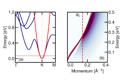
For concentrations of -type carriers larger than cm-2, MoS2 undergoes a metal-insulator transition 36, characterized by the onset of metallic transport properties 37 and by the partial filling of the K valley in the conduction band. The conduction-band dispersion of monolayer MoS2 as obtained from density-functional theory calculations is reported in Fig. 2 (a). The Fermi energy of the doped system depends linearly on the carrier concentration via the expression , with being the K-valley degeneracy, and the energy of the CBm. For the experimentally determined Fermi energies , , and meV, this expression allows one to determine the carrier concentrations , , and respectively. For , the Fermi energy is marked by the horizontal dashed line in Fig. 2 (a). Upon interaction with light, extrinsic carriers in the conduction band can be collectively excited leading to well-defined 2D carrier plasmon resonances. The energy-momentum dispersion relation of 2D plasmons in MoS2 is here approximated by the loss function of a 2D homogeneous electron gas (2HEG) 38, 39. All calculations have been conducted using the experimental effective mass (with being the bare electron mass), which has been obtained by ARPES measurements of the conduction band of monolayer MoS2 single-crystals (see Supplementary Note 3 and Fig. S1). The influence of on the calculations and on electron-plasmon interaction is discussed in Supplementary Note 4 and Fig. S2-S3. We further explicitly account for the extrinsic dielectric environment induced by the semi-infinite sapphire (Al2O3) substrate by introducing the dielectric constant , with being the high-frequency dielectric constant of bulk sapphire 40.
The loss function, illustrated in Fig. 2 (b) for the carrier concentration , exhibits pronounced plasmon peaks, with plasmon energies ranging from 0 to 0.24 eV. Only plasmons with momenta can be excited, where Å-1 (marked by a dashed vertical line in Fig. 2 (b)) is the critical momentum for the onset of Landau damping, namely, the decay of plasmons upon excitation of electron-hole pairs. The plasmon dispersion obtained from the loss function compares well with the analytical result for homogeneous 2D metals 41, illustrated in Fig. 2 (b) as a continuous line. Here, and .
In systems characterized by electronic coupling to weakly-dispersive bosonic modes (as, e.g., optical phonons or 3D plasmons) the energy of polaronic satellites can be directly related to the boson energy. Therefore, at a first sight it might seem surprising that the coupling to 2D plasmons could give rise to a satellite peak with a well-defined energy, since the 2D plasmon dispersion continuously spans the energy range between 0 and 240 meV (Fig. 2 (b)). To clarify this aspect, we show in the following that the satellite energy is related to the average energy of 2D plasmons in the Brillouin zone. This finding leads us to the interpretation of the measured ARPES satellite as a result of the collective coupling to all 2D plasmons in the system, rather than to a single bosonic excitation. To estimate the average energy of 2D plasmons, we consider the density of states of plasmonic excitations:
| (1) |
where and is the plasmon energy at the critical momentum . This result may be promptly verified by analytical integration of Eq. (1), as illustrated in the SI. For , , and , the density of states is illustrated in Fig. S11. From Eq. (1), we can estimate the average plasmon energy as and the standard deviation . For , the value eV yields meV which agrees well with the effective boson energy meV derived from the satellite energy. Similarly, the spread of the plasmon energies in the Brillouin zone is quantified by meV, which is in good agreement with the half width at half maximum of the satellite peak meV, which we extract from Gaussian decomposition of the experimental spectra. This analysis suggests that the observation of a well-defined satellite in ARPES is compatible with a bosonic coupling mechanism induced by 2D carrier plasmons. In particular, the satellite energy can be related to the average energy of 2D plasmons, whereas the satellite linewidth reflects the spread of plasmon energies as quantified by the standard deviation .
To quantitatively demonstrate the influence of the electron-plasmon interaction on ARPES measurements, we conducted first-principles calculations of the spectral function based on the cumulant expansion approach 42, 43, 44, the state of the art for spectral-function calculations of coupled electron-boson systems 45. The cumulant spectral function can be expressed as 22:
| (2) |
where denotes convolution over frequency, and is the quasiparticle contribution to the spectral function. is the single-particle energy, and is the electron self-energy due to the electron-plasmon interaction, for which an explicit expression is given in the SI. Dynamical correlations due to the electron-plasmon interaction are accounted for by the satellite function :
| (3) |
with , and the dependence on and has been omitted. Computational details are reported in Supplementary Note 6.
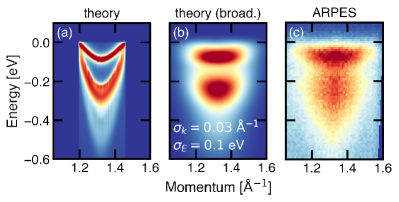
The cumulant spectral function of -doped MoS2 is illustrated in Figs. 1 (c)-(d) as a red line for and , respectively. The spectral function for a broader range of carrier densities is illustrated in Fig. S10 (b). Remarkably, the increase of the satellite energy with carrier concentration is in excellent agreement with the calculated trend (see Fig. S10 (a)). The experimental background signal has been added to theoretical data to facilitate the comparison. The calculated spectral function exhibits two distinct satellite resonances at energies in excellent agreement with the ARPES spectral features. The Taylor expansion of Eq. (2) up to second order in promptly reveals the physical origin of these spectral features: beside the quasiparticle peak, arising from alone, the second term in the expansion stems from the convolution , and its intensity may be attributed to the rate of photoemission processes resulting from the coupled excitation of a photo-hole and a plasmon. Similarly, subsequent arguments in the Taylor expansion can be related to multiple plasmon excitations. This allows us to relate subsequent satellites to photoemission processes resulting from the simultaneous excitation a photo-hole and emission of plasmons. The quantitative agreement between experiment and theory is further illustrated in Fig. 3, where the full calculated and measured angle-resolved spectral functions are compared for the carrier concentration cm-2. Finite experimental resolution for energy (momentum) is explicitly accounted for in Fig. 3 (b) by convolution with a Gaussian function with full-width at half maximum of 100 meV (0.03 Å-1). The calculated satellite structure is sharper as compared to the measurements, since our calculations do not explicitly account for finite lifetime effects in the plasmon dispersion arising from the plasmon-phonon scattering. Scattering between plasmons and phonons can indeed lower the plasmon lifetime, introducing additional broadening of the plasmon satellite 39.
In conclusion, we reported the observation of 2D plasmonic polarons in -doped monolayer MoS2 at degenerate doping concentrations. The emergence of distinctive signatures of polaronic satellites in ARPES experiments provides compelling evidence of the strong coupling between 2D carrier plasmons and extrinsic carriers, and it is corroborated by first-principles calculations of the electron-plasmon interaction. This finding indicates that, at sufficiently large doping concentrations, the quantum confinement of holes and plasmons in a 2D semiconductor triggers the onset of a strong-coupling regime, whereby electron-plasmon coupling results in the formation of 2D plasmonic polarons.
This work was funded by the Deutsche Forschungsgemeinschaft (DFG) – Projektnummer 182087777 – SFB 951. FC acknowledges useful discussions with Pasquale Pavone. AA and VT are indebted to the support from the KAUST Office of Sponsored Research (OSR) under Award No: OSR-2018-CARF/CCF-3079. MZ acknowledges support by the Research Promotion Foundation of the Republic of Cyprus under Award: NEW INFRASTRUCTURE/TPATH/0308/04 and the DECI resource Saniyer at UHeM based in Turkey [http://en.uhem.itu.edu.tr] with support from the PRACE aisbl.
Supporting Information Available: The Supporting Information is available free of charge at \urllink to be added by publisher.46, 47, 48, 49, 50, 51, 52, 53, 54, 55, 56, 57, 58, 59 Supplementary Notes 1-6; Supplementary Figures S1-S12.
References
- Mak et al. 2010 Mak, K. F.; Lee, C.; Hone, J.; Shan, J.; Heinz, T. F. Atomically Thin : A New Direct-Gap Semiconductor. Phys. Rev. Lett. 2010, 105, 136805
- Qiu et al. 2013 Qiu, D. Y.; da Jornada, F. H.; Louie, S. G. Optical Spectrum of : Many-Body Effects and Diversity of Exciton States. Phys. Rev. Lett. 2013, 111, 216805
- Molina-Sánchez et al. 2016 Molina-Sánchez, A.; Palummo, M.; Marini, A.; Wirtz, L. Temperature-dependent excitonic effects in the optical properties of single-layer . Phys. Rev. B 2016, 93, 155435
- Hong et al. 2020 Hong, J.; Senga, R.; Pichler, T.; Suenaga, K. Probing Exciton Dispersions of Freestanding Monolayer by Momentum-Resolved Electron Energy-Loss Spectroscopy. Phys. Rev. Lett. 2020, 124, 087401
- Mak et al. 2013 Mak, K. F.; He, K.; Lee, C.; Lee, G. H.; Hone, J.; Heinz, T. F.; Shan, J. Tightly bound trions in monolayer MoS2. Nature Mater. 2013, 12, 207–211
- Kang et al. 2018 Kang, M.; Jung, S. W.; Shin, W. J.; Sohn, Y.; Ryu, S. H.; Kim, T. K.; Hoesch, M.; Kim, K. S. Holstein polaron in a valley-degenerate two-dimensional semiconductor. Nature Mater. 2018, 17, 676
- Garcia-Goiricelaya et al. 2019 Garcia-Goiricelaya, P.; Lafuente-Bartolome, J.; Gurtubay, I. G.; Eiguren, A. Long-living carriers in a strong electron–phonon interacting two-dimensional doped semiconductor. Commun. Phys. 2019, 2, 81
- Zheng et al. 2017 Zheng, D.; Zhang, S.; Deng, Q.; Kang, M.; Nordlander, P.; Xu, H. Manipulating Coherent Plasmon–Exciton Interaction in a Single Silver Nanorod on Monolayer WSe2. Nano Lett. 2017, 17, 3809–3814
- Stührenberg et al. 2018 Stührenberg, M.; Munkhbat, B.; Baranov, D. G.; Cuadra, J.; Yankovich, A. B.; Antosiewicz, T. J.; Olsson, E.; Shegai, T. Strong Light–Matter Coupling between Plasmons in Individual Gold Bi-pyramids and Excitons in Mono- and Multilayer WSe2. Nano Lett. 2018, 18, 5938–5945
- Gonçalves et al. 2018 Gonçalves, P. A. D.; Bertelsen, L. P.; Xiao, S.; Mortensen, N. A. Plasmon-exciton polaritons in two-dimensional semiconductor/metal interfaces. Phys. Rev. B 2018, 97, 041402
- Liu et al. 2018 Liu, W.; Wang, Y.; Naylor, C. H.; Lee, B.; Zheng, B.; Liu, G.; Johnson, A. T. C.; Pan, A.; Agarwal, R. Understanding the Different Exciton–Plasmon Coupling Regimes in Two-Dimensional Semiconductors Coupled with Plasmonic Lattices: A Combined Experimental and Unified Equation of Motion Approach. ACS Photon. 2018, 5, 192–204
- Cuadra et al. 2018 Cuadra, J.; Baranov, D. G.; Wersäll, M.; Verre, R.; Antosiewicz, T. J.; Shegai, T. Observation of Tunable Charged Exciton Polaritons in Hybrid Monolayer WS2-Plasmonic Nanoantenna System. Nano Lett. 2018, 18, 1777–1785
- Costanzo et al. 2016 Costanzo, D.; Jo, S.; Berger, H.; Morpurgo, A. F. Gate-induced superconductivity in atomically thin MoS2 crystals. Nature Nanotechol. 2016, 11, 339–344
- Latini et al. 2019 Latini, S.; Ronca, E.; De Giovannini, U.; Hübener, H.; Rubio, A. Cavity Control of Excitons in Two-Dimensional Materials. Nano Lett. 2019, 19, 3473–3479
- Cao et al. 2012 Cao, T.; Wang, G.; Han, W.; Ye, H.; Zhu, C.; Shi, J.; Niu, Q.; Tan, P.; Wang, E.; Liu, B. et al. Valley-selective circular dichroism of monolayer molybdenum disulphide. Nature Commun. 2012, 3, 887
- Beyer et al. 2019 Beyer, H.; Rohde, G.; Grubišić Čabo, A.; Stange, A.; Jacobsen, T.; Bignardi, L.; Lizzit, D.; Lacovig, P.; Sanders, C.; Lizzit, S. et al. 80% Valley Polarization of Free Carriers in Singly Oriented Single-Layer WS 2 on Au(111). Phys. Rev. Lett. 2019, 123, 236802
- Kang et al. 2015 Kang, K.; Xie, S.; Huang, L.; Han, Y.; Huang, P. Y.; Mak, K. F.; Kim, C.-J.; Muller, D.; Park, J. High-mobility three-atom-thick semiconducting films with wafer-scale homogeneity. Nature 2015, 520, 656–660
- Briggs et al. 2020 Briggs, N.; Bersch, B.; Wang, Y.; Jiang, J.; Koch, R. J.; Nayir, N.; Wang, K.; Kolmer, M.; Ko, W.; De La Fuente Duran, A. et al. Atomically thin half-van der Waals metals enabled by confinement heteroepitaxy. Nature Mater. 2020, 19, 637–643
- Moser et al. 2013 Moser, S.; Moreschini, L.; Jaćimović, J.; Barišić, O. S.; Berger, H.; Magrez, A.; Chang, Y. J.; Kim, K. S.; Bostwick, A.; Rotenberg, E. et al. Tunable Polaronic Conduction in Anatase . Phys. Rev. Lett. 2013, 110, 196403
- Wang et al. 2016 Wang, Z.; McKeown Walker, S.; Tamai, A.; Wang, Y.; Ristic, Z.; Bruno, F. Y.; de la Torre, A.; Riccò, S.; Plumb, N. C.; Shi, M. et al. Tailoring the nature and strength of electron-phonon interactions in the SrTiO3(001) two-dimensional electron liquid. Nat. Mater. 2016, 15, 835–839
- Janotti et al. 2014 Janotti, A.; Varley, J. B.; Choi, M.; Van de Walle, C. G. Vacancies and small polarons in . Phys. Rev. B 2014, 90, 085202
- Verdi et al. 2017 Verdi, C.; Caruso, F.; Giustino, F. Origin of the crossover from polarons to Fermi liquids in transition metal oxides. Nat. Commun. 2017, 8, 15769
- Moses et al. 2016 Moses, P. G.; Janotti, A.; Franchini, C.; Kresse, G.; Van de Walle, C. G. Donor defects and small polarons on the TiO2(110) surface. J. Appl. Phys. 2016, 119, 181503
- Chen et al. 2018 Chen, C.; Avila, J.; Wang, S.; Wang, Y.; Mucha-Kruczyński, M.; Shen, C.; Yang, R.; Nosarzewski, B.; Devereaux, T. P.; Zhang, G. et al. Emergence of Interfacial Polarons from Electron–Phonon Coupling in Graphene/h-BN van der Waals Heterostructures. Nano Lett. 2018, 18, 1082–1087
- Riley et al. 2018 Riley, J. M.; Caruso, F.; Verdi, C.; Duffy, L. B.; Watson, M. D.; Bawden, L.; Volckaert, K.; van der Laan, G.; Hesjedal, T.; Hoesch, M. et al. Crossover from lattice to plasmonic polarons of a spin-polarised electron gas in ferromagnetic EuO. Nature Commun. 2018, 9, 2305
- Caruso et al. 2018 Caruso, F.; Verdi, C.; Poncé, S.; Giustino, F. Electron-plasmon and electron-phonon satellites in the angle-resolved photoelectron spectra of -doped anatase . Phys. Rev. B 2018, 97, 165113
- Sio et al. 2019 Sio, W. H.; Verdi, C.; Poncé, S.; Giustino, F. Polarons from First Principles, without Supercells. Phys. Rev. Lett. 2019, 122, 246403
- Sio et al. 2019 Sio, W. H.; Verdi, C.; Poncé, S.; Giustino, F. Ab initio theory of polarons: Formalism and applications. Phys. Rev. B 2019, 99, 235139
- Amsalem et al. 2020 Amsalem, P.; Ma, J.; Schultz, T., et al. submitted 2020,
- Aljarb et al. 2017 Aljarb, A.; Cao, Z.; Tang, H.-L.; Huang, J.-K.; Li, M.; Hu, W.; Cavallo, L.; Li, L.-J. Substrate Lattice-Guided Seed Formation Controls the Orientation of 2D Transition-Metal Dichalcogenides. ACS Nano 2017, 11, 9215–9222
- Baugher et al. 2013 Baugher, B. W. H.; Churchill, H. O. H.; Yang, Y.; Jarillo-Herrero, P. Intrinsic Electronic Transport Properties of High-Quality Monolayer and Bilayer MoS2. Nano Lett. 2013, 13, 4212–4216
- Schuler et al. 2019 Schuler, B.; Qiu, D. Y.; Refaely-Abramson, S.; Kastl, C.; Chen, C. T.; Barja, S.; Koch, R. J.; Ogletree, D. F.; Aloni, S.; Schwartzberg, A. M. et al. Large Spin-Orbit Splitting of Deep In-Gap Defect States of Engineered Sulfur Vacancies in Monolayer . Phys. Rev. Lett. 2019, 123, 076801
- Liu et al. 2017 Liu, M.; Shi, J.; Li, Y.; Zhou, X.; Ma, D.; Qi, Y.; Zhang, Y.; Liu, Z. Temperature-Triggered Sulfur Vacancy Evolution in Monolayer MoS2/Graphene Heterostructures. Small 2017, 13, 1602967
- Park et al. 2019 Park, S.; Schultz, T.; Han, A.; Aljarb, A.; Xu, X.; Beyer, P.; Opitz, A.; Ovsyannikov, R.; Li, L.-J.; Meissner, M. et al. Electronic band dispersion determination in azimuthally disordered transition-metal dichalcogenide monolayers. Commun. Phys. 2019, 2, 68
- Anderson 1990 Anderson, O. Deconvolution of UPS and XPS spectra. Vacuum 1990, 41, 1700 – 1702
- Mott 1968 Mott, N. F. Metal-Insulator Transition. Rev. Mod. Phys. 1968, 40, 677–683
- Radisavljevic and Kis 2013 Radisavljevic, B.; Kis, A. Mobility engineering and a metal–insulator transition in monolayer MoS2. Nat. Mater. 2013, 12, 815
- Caruso and Giustino 2016 Caruso, F.; Giustino, F. The GW plus cumulant method and plasmonic polarons: application to the homogeneous electron gas*. Eur. Phys. J. B 2016, 89, 238
- Caruso et al. 2018 Caruso, F.; Novko, D.; Draxl, C. Phonon-assisted damping of plasmons in three- and two-dimensional metals. Phys. Rev. B 2018, 97, 205118
- Fontanella et al. 1974 Fontanella, J.; Andeen, C.; Schuele, D. Low‐frequency dielectric constants of -quartz, sapphire, MgF2, and MgO. J. Appl. Phys. 1974, 45, 2852–2854
- Giuliani and Vignale 2005 Giuliani, G. F.; Vignale, G. Quantum theory of the electron liquid; Cambridge Univ. Press: Cambridge, 2005
- Langreth 1970 Langreth, D. C. Singularities in the X-Ray Spectra of Metals. Phys. Rev. B 1970, 1, 471–477
- Aryasetiawan et al. 1996 Aryasetiawan, F.; Hedin, L.; Karlsson, K. Multiple Plasmon Satellites in Na and Al Spectral Functions from ab initio Cumulant Expansion. Phys. Rev. Lett. 1996, 77, 2268–2271
- Guzzo et al. 2011 Guzzo, M.; Lani, G.; Sottile, F.; Romaniello, P.; Gatti, M.; Kas, J. J.; Rehr, J. J.; Silly, M. G.; Sirotti, F.; Reining, L. Valence Electron Photoemission Spectrum of Semiconductors: Ab Initio Description of Multiple Satellites. Phys. Rev. Lett. 2011, 107, 166401
- Caruso et al. 2018 Caruso, F.; Verdi, C.; Giustino, F. Handbook of Materials Modeling; Springer, Berlin, 2018
- Giannozzi et al. 2017 Giannozzi, P.; Andreussi, O.; Brumme, T.; Bunau, O.; Nardelli, M. B.; Calandra, M.; Car, R.; Cavazzoni, C.; Ceresoli, D.; Cococcioni, M. et al. Advanced capabilities for materials modelling with Quantum ESPRESSO. J. Phys: Condens. Matter 2017, 29, 465901
- Molina-Sánchez et al. 2013 Molina-Sánchez, A.; Sangalli, D.; Hummer, K.; Marini, A.; Wirtz, L. Effect of spin-orbit interaction on the optical spectra of single-layer, double-layer, and bulk MoS2. Phys. Rev. B 2013, 88, 045412
- Poncé et al. 2016 Poncé, S.; Margine, E.; Verdi, C.; Giustino, F. EPW: Electron–phonon coupling, transport and superconducting properties using maximally localized Wannier functions. Comput. Phys. Commun. 2016, 209, 116 – 133
- Mostofi et al. 2008 Mostofi, A. A.; Yates, J. R.; Lee, Y.-S.; Souza, I.; Vanderbilt, D.; Marzari, N. wannier90: A tool for obtaining maximally-localised Wannier functions. Comput. Phys. Commun. 2008, 178, 685 – 699
- Marzari et al. 2012 Marzari, N.; Mostofi, A. A.; Yates, J. R.; Souza, I.; Vanderbilt, D. Maximally localized Wannier functions: Theory and applications. Rev. Mod. Phys. 2012, 84, 1419–1475
- Pines and Schrieffer 1962 Pines, D.; Schrieffer, J. R. Approach to Equilibrium of Electrons, Plasmons, and Phonons in Quantum and Classical Plasmas. Phys. Rev. 1962, 125, 804–812
- Caruso and Giustino 2016 Caruso, F.; Giustino, F. Theory of electron-plasmon coupling in semiconductors. Phys. Rev. B 2016, 94, 115208
- Anemone et al. 2019 Anemone, G.; Taleb, A. A.; Benedek, G.; Castellanos-Gomez, A.; Farías, D. Electron–Phonon Coupling Constant of 2H-MoS2(0001) from Helium-Atom Scattering. J. Phys. Chem. C 2019, 123, 3682–3686
- Filip et al. 2015 Filip, M. R.; Verdi, C.; Giustino, F. GW Band Structures and Carrier Effective Masses of CH3NH3PbI3 and Hypothetical Perovskites of the Type APbI3: A = NH4, PH4, AsH4, and SbH4. J. Phys. Chem. C 2015, 119, 25209–25219
- Poncé et al. 2018 Poncé, S.; Margine, E. R.; Giustino, F. Towards predictive many-body calculations of phonon-limited carrier mobilities in semiconductors. Phys. Rev. B 2018, 97, 121201
- Popescu and Zunger 2012 Popescu, V.; Zunger, A. Extracting versus effective band structure from supercell calculations on alloys and impurities. Phys. Rev. B 2012, 85, 085201
- Medeiros et al. 2014 Medeiros, P. V. C.; Stafström, S.; Björk, J. Effects of extrinsic and intrinsic perturbations on the electronic structure of graphene: Retaining an effective primitive cell band structure by band unfolding. Phys. Rev. B 2014, 89, 041407
- Zacharias and Giustino 2020 Zacharias, M.; Giustino, F. Theory of the special displacement method for electronic structure calculations at finite temperature. Phys. Rev. Res. 2020, 2, 013357
- Jeong et al. 2019 Jeong, T. Y.; Kim, H.; Choi, S.-J.; Watanabe, K.; Taniguchi, T.; Yee, K. J.; Kim, Y.-S.; Jung, S. Spectroscopic studies of atomic defects and bandgap renormalization in semiconducting monolayer transition metal dichalcogenides. Nature Commun. 2019, 10, 3825