Ab initio study of anisotropic mechanical and electronic properties of strained carbon-nitride nanosheet with interlayer bonding
Abstract
Due to the noticeable structural similarity and being neighborhood in periodic table of group-IV and -V elemental monolayers, whether the combination of group-IV and -V elements could have stable nanosheet structures with optimistic properties has attracted great research interest. In this work, we performed first-principles simulations to investigate the elastic, vibrational and electronic properties of the carbon nitride (CN) nanosheet in the puckered honeycomb structure with covalent interlayer bonding. It has been demonstrated that the structural stability of CN nanosheet is essentially maintained by the strong interlayer bonding between adjacent carbon atoms in the opposite atomic layers. A negative Poisson’s ratio in the out-of-plane direction under biaxial deformation, and the extreme in-plane stiffness of CN nanosheet, only slightly inferior to the monolayer graphene, are revealed. Moreover, the highly anisotropic mechanical and electronic response of CN nanosheet to tensile strain have been explored.
- DOI
I Introduction
The fascinating mechanical and electronic properties of monolayer graphene and its heterostructures, derived from its unique hexagonal symmetry with intralayer bonding, such as high carrier mobility, massless Dirac fermions, and ultrastrength in-plane stiffness, have attracted significant research interest in two-dimensional (2D) materials for the last decade [1, 2, 3]. Not only have the extraordinary properties of monolayer graphene been revealed, but also the existence of other group-IV elements forming honeycomb lattices, i.e., silicene and germanene, has been demonstrated [4, 5]. However, the electronic application of group-IV element monolayer is limited by the band gap closure around the Fermi level [6]. Recent synthesis of phosphorene has demonstrated the actual existence of group-V elemental monolayer and its intriguing properties, such as direct band gap, high carrier mobility, and prevalent optical properties have been revealed [7, 8, 9]. Besides, the theoretical predictions of stability, electronic structures [10, 11] and experimental synthesis [11] of group-III element monolayers have been systematically studied. Because of their noticeable structural similarity and being neighborhood in periodic table of group-IV and -V elemental monolayers, one would ask, whether the compounds consisting of group-IV and -V elements could have stable nanosheet structures with optimistic properties. Plentiful attempts have been directed towards synthesizing group IV-V compounds, e.g., carbon nitride (CN) and carbon phosphide (CP), from three-dimensional (3D) bulk phases to 2D nanosheets [12]. Some experiment results have manifested the existence of - showing comparable hardness to diamond [13, 14, 15]. Moreover, the possibility of a wide range of other nitrogen concentration is shown in other experimental data [16, 17]. The synthesis of amorphous CP films using radio frequency plasma deposition method has been reported by Pearce et al. [18] Different C/P ratios can be achieved by adjusting the ratio of PH3/CH4 gas during the synthesis. In other experiments, the pulsed laser deposition [19, 20] and magnetron sputtering techniques [21] were used in producing CP films.
Several possible crystal structures for CN bulk phase have been suggested via theoretical study, including the eight structures considered by Cote and Cohen, among which the GaSe layered phase (honeycomb crystal) is assumed to be the most energetically favorable structure [22]. Besides that, in our earlier work [23], it is predicted that the GaSe layered phase are energetically favorable for all group IV-V compounds except for SnSb, and it shows semiconductor characters while other structures show metallic properties. For 2D nanosheets, Wang et al. suggested three kinds of potential structures for CP which they calculated super carrier mobility and strong anisotropy [24]. On the other hand, the electronic and thermal properties of multi-layer nanosheets and its heterostructures are substantially affected by the interlayer interaction [25, 26, 27, 28, 29]. There are generally two ways for layer interactions, Van der Walls (vdW) force and covalent bonding. The covalent bonding naturally brings in stronger cross-plane coupling than the weak vdW force. Recent experiments have shown that the bonding of C atoms between the layers of graphite could be induced by visible-light irradiation [30]. The cooperative and nonlinear formation mechanisms of this excited interlayer bonds are demonstrated [31]. The influence of these interlayer interaction to the thermal properties of multi-layer graphene has been conducted both experimentally and theoretically [32, 33, 34].
In this paper, we performed first-principles simulations to investigate the elastic, vibrational and electronic properties of the CN nanosheet in the puckered honeycomb structure with covalent interlayer bonding. It has been demonstrated that the structure stability of CN nanosheets is essentially maintained by the strong interlayer bonding between two adjacent carbon atoms in the opposite atomic layers. Our numerical results show a negative Poisson’s ratio in the out-of-plane direction under biaxial deformation. We attribute this abnormal Poisson’s ratio to the introduction of additional degrees of out-of-plane atomic relaxations by the formation of covalent interlayer bonding in CN nanosheet. With the application of various uniaxial and biaxial tension strains, the highly anisotropic mechanical and electronic response of CN nanosheet to the the strain has been explored. It is identified that the tensile strength of CN nanosheets are dictated by the instability of out-of-plane transverse phonon branch ZA for armchair tension , but in-plane transverse phonon branch TA for the zigzag tension . Our calculations indicate that the indirect band gap of CN nanosheet could be significantly tailored through strain engineering which manifests its potential application in the optoelectronic fields.
II Method
We carried out the first-principles calculations based on the density functional theory (DFT) as implemented in the Quantum Espresso simulation package [35]. The Perdew-Burke-Ernzerhof (PBE) exchange-correlation functional [36] along with the projector augmented wave (PAW) pseudopotentials [37] were adopted for the self-consistent total energy and electronic-structure calculations. The kinetic energy cutoff for wave functions and charge density were set to be 85 Ry and 595 Ry respectively. To model CN nanosheets, a four-atom primitive cell containing two carbon atoms and two nitrogen atoms was chosen with periodic boundary condition applied (see Fig. 1). Specifically, for stress-strain calculations, an eight-atom orthogonal unit cell was employed to achieve uniaxial stress along the armchair and zigzag direction (Fig. 1, dashed boxes). A Monkhorst-Pack grid of () -points was used to sample the first reciprocal Brillouin Zone (BZ). The energy convergence criteria for electronic and ionic iterations were set to be Ry and Ry, respectively. All atomic positions and unit cell were optimized until the atomic forces were less than . A minimum of 20 Å vacuum spacing in the out-of-plane direction was applied to prevent interaction from adjacent supercells. The phonon dispersion curves were calculated by diagonalizing the dynamical matrix based on the density functional perturbation theory.
It is well known that the PBE functional may underestimate the calculated band gaps. In this work, the frequency-dependent quasiparticle calculations were performed to correct the ground state band gaps obtained by PBE. Furthermore, a scissors operator method has been implemented to correct band gaps under tensile strains [38, 39]. The calculations were conducted as a “one-shot” correction to self-consistent PBE calculations. This approach, denoted as , has yielded remarkably accurate band structures for many materials [40, 41, 42]. Various tests were carried out to achieve convergence regarding -points, vacuum level, number of bands, and kinetic energy cutoff. Final corrections on the PBE bands gaps were obtained by using () -points in BZ, 25 Å vacuum spacing, 120 bands and default cut-off potential for .
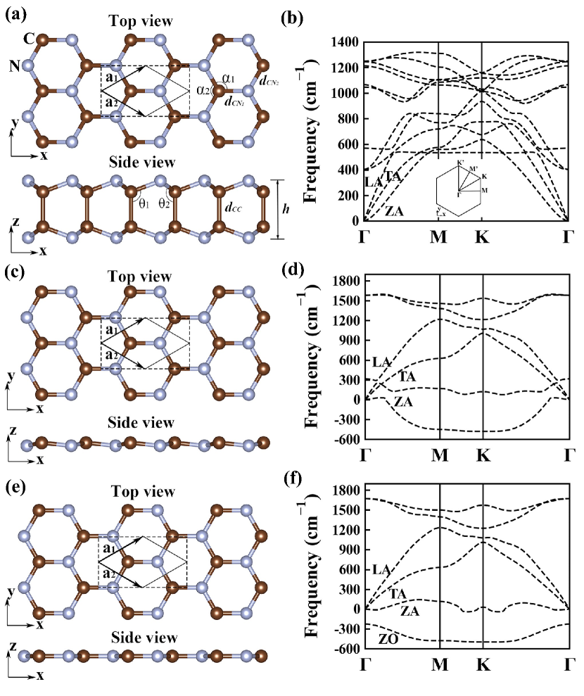
In contrast to the flatness of graphene, the CN nanosheet we proposed here is a puckered honeycomb structure with covalent interlayer bonding. The bravais lattice vectors of primitive cell are defined as and , shown in Fig. 1(a). The armchair and zigzag directions are along the and directions, respectively. Under uniaxial tension, the original lattice symmetry is broken, thus the structure parameters along armchair direction and zigzag direction are different (the subscripts are assigned to distinguish them). The intralayer bonding and are formed between carbon and nitrogen atoms in the same atomic layer, while the interlayer bonding is formed between two adjacent carbon atoms in the opposite atomic layers. The in-plane N-C-N bond angles is named as and , and out-of-plane N-C-C bond angle is named as and , respectively. The layer height of CN nanosheet is characterized by the atomic distance between two nitrogen atoms sited opposite in the out-of-plane direction, i.e., . The first BZ is deformed under the uniaxial tension with high symmetry points splitting up, as shown in Fig. 1(b).
For the stress-strain relations, in order to make a direct comparison of 2D nanosheets with experiments and other theoretical results, we need to rescale the supercell stress by to obtain the equivalent stress, where is the cell length in the direction perpendicular to atomic layers and is the effective thickness of nanosheet. In this work, we take Å for CN nanosheet which is the equilibrium interlayer spacing of CN bulk phase calculated in previous work by Cohen et al. [22] It is worthwhile to mention that the vdW interactions between adjacent atomic layers of CN nanosheet are neglected in our calculations because those vdW corrections are assumed to be much weaker than the covalent interlayer bonding of CN nanosheet [25].
III Results
We first optimize the equilibrium structural parameters of CN nanosheets in 2D honeycomb lattices. In present work, we consider three atomic configurations in accordance with the rate of buckling in the out-of-plane direction, i.e., low-buckled (LB) (or puckered) geometry with covalent interlayer bonding, LB geometry without interlayer bonding, and planar (PL) geometry. The structural stabilities of these three atomic configurations are examined by calculating the phonon dispersion curves.
Figure. 1 shows the optimized structure models along with the ground state phonon dispersion curves of these three atomic configurations of CN nanosheets. While the LB geometry without interlayer bonding and PL geometry both show imaginary (negative) frequencies in the phonon dispersion, the structural stability is exclusively attained by the LB geometry with covalent interlayer bonding . Compared to the planar geometry, the out-of-plane transverse phonon branch ZO is stabilized through the buckling of C-N atomic layers in the LB geometry [Fig. 1(d) and 1(f)]. The planar orbital is slightly dehybridized with perpendicular orbital to form a -like orbital as a result of the buckling. This buckled stabilization mechanism could be interpreted as the in-plane bonding formed between C and N atoms is not strong enough to maintain the planar geometry by comparison with the C-C bonding in the monolayer graphene [43]. However, it is still unstable with respect to the out-of-plane transverse phonon branch ZA in the LB geometry without interlayer bonding. Through the coupling of two symmetrically buckled atomic layers in hexagonal lattice, as the formation of covalent interlayer bonds between two adjacent C atoms, the CN nanosheets is stabilized with fourfold bonding of C atoms and threefold bonding of N atoms [Fig. 1(b) and 1(d)]. The coordination number of C and N atoms are consistent with the number of valence electrons needed to fully fill their electronic shell respectively. In contrast to the weak vdW interactions between few layers planar graphene, this strong interlayer bonding between C atoms together with the buckled C-N atomic layers maintain the structure stability of CN nanosheet. Besides that, It is further confirmed by the comparison of the calculated cohesive energy among these three atomic configurations. The cohesive energy is defined as , where is the total energy per pair atoms of optimized CN nanosheet; and are the total energies of isolated C and N atoms corresponding to nonmagnetic state. The cohesive energy of LB geometry with covalent interlayer bonding, eV/atom, turns out to be much larger than other two atomic configurations without interlayer bonding (Table SI, supplementary material). Consequently, from the indication of structure stability analysis above, our theoretical results below will be built based on the LB geometry with covalent interlayer bonding .
| Structure | (°) | (°) | (Å) | (Å) | (Å) | (Å) | (eV/atom) | |
| CN | 110.3 | 108.6 | 1.46 | 1.63 | 2.38 | 2.65 | 8.36 |
Table. 1 summarizes the calculated equilibrium structural parameters of CN nanosheet. It is interesting to compare the lattice parameters of CN nanosheet with those of graphene and other hexagonal lattice structures. The bond length of intralayer C-N bond of CN nanosheet, Å, is approaching that of the C-C bond in monolayer graphene (1.44 Å) and B-N bond in boron nitride (1.45 Å), both having very high in-plane strength, but much shorter than the Mo-S bond in (2.42 Å) and all other potential hexagonal structure of binary monolayer of group-IV elements and group III-V compounds reported by Şahain et al.[43] As for the interlayer C-C bond, Å, it is a bit longer than the bond length of hybridized orbital in diamond (1.53 Å). In addition, the in-plane bond angle and out-of-plane bond angle are 108.6° and 110.3° respectively, which are quite close to that of 109.5° in diamond. Briefly, the strong interlayer bonding together with the hybridized -like orbital underlie unusual in-plane and out-of-plane mechanical strength of CN nanosheet compared to other traditional 2D materials.
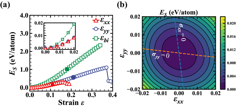
To further explore the impact of strain on vibrational, mechanical and electronic properties of CN nanosheet, we then stretch the eight-atom unit cell of CN with a series of incremental tensile strains including uniaxial tension along (armchair) direction , uniaxial tension along (zigzag) direction , and biaxial tension (). The atomic positions for each step are taken from the relaxed coordinates of the former step to ensure the continuity of strain path. For the uniaxial tension, the optimized structures are attained by simultaneously relaxing the strain components orthogonal to the applied strain. The variation in strain energies, , by subtracting the total energy per atom of the deformed structure from the equilibrium one, is obtained as functions of elastic strain in both harmonic and anharmonic domain. Owing to the hexagonal symmetry of honeycomb structure, CN nanosheet shows isotropic strain energy response at small strains [inset in Fig. 2(a)]. In Fig. 2(b), we show the contour plot of strain energy as functions of strains (). The energy-strain relation is then obtained as a quadratic polynomial , where , , and are parameters to be fitted. With the small strain limit, we set as CN nanosheet is elastically isotropic within the plane. The elastic stiffness constants can then be expressed in terms of these fitting parameters, i.e., ; . Hence, the effective Young’s modulus can be obtained as, , where are the equilibrium surface area of the system. The CN nanosheet is calculated to have an effective Young’s modulus GPa which is comparable to that of 1 TPa in monolayer graphene [44, 45].
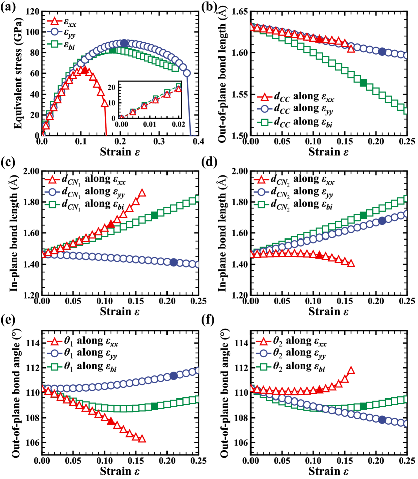
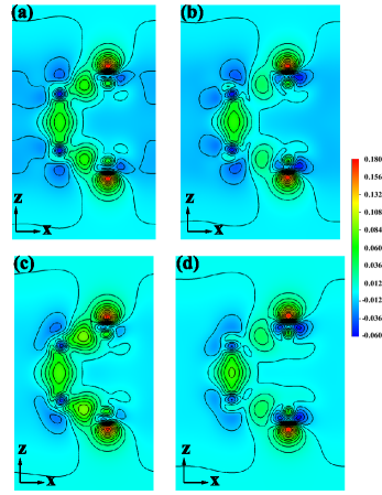
Furthermore, we calculate the ideal strength of CN nanosheet under tensile strain. Figure. 3(a) shows the equivalent stress as functions of tensile strains for CN nanosheet. Similar to the strain energy response, CN nanosheet has isotropic in-plane elastic response at small strains. There is no observable difference of the elastic response between the uniaxial tension and when strains are less than 0.02. While, at large strains, due to the broken of lattice symmetry, the elastic response in armchair direction becomes distinct from zigzag direction. The maximum stress for uniaxial tension along armchair direction is , at . Compared to that, CN nanosheet is stronger in the zigzag direction with maximum stress , at . Thus, we predict that the zigzag direction is 41% stronger than the armchair direction and can sustain 91% more strain. For the biaxial tension, the maximum stress is 82 GPa, at , which is between that along the armchair and zigzag tensions. It is worth mentioned that the ideal strength of CN nanosheet in armchair and zigzag direction are both smaller than those of 110 GPa and 121 GPa in monolayer graphene [46], but approaching that of 88 GPa and 102 GPa in single-layer hexagonal BN [47]. Moreover, we have explored the responses of the atomic relaxations, i.e., bond length and bond angle, with respect to the tensile strains, shown in Fig. 3(b-f). Most structure parameters show similar trend of variation (linear and monotonic) with respect to the tensions, especially within small strains. However, it is noted that the out-of-plane bond angle shows non-monotonic response (negative to positive slop ratio) with respect to the biaxial tension. This unique mechanical response indicates that there is competition between in-plane and out-of-plane atomic relaxation under tensile strain. The plot of deformation charge density gives a more vivid understanding of the variations of structure versus the tensile strains, as shown in Fig. 4. In the analysis of Poisson’s ratio, we will give further explanation about the competition mechanism of this unique mechanical response.
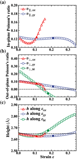
The finite-deformation Poisson’s ratio is defined as the ratio of the transverse strain to the applied strain [46, 43]. The in-plane Poisson’s ratio is thus well defined as and where the prime symbol denotes the relaxed strain. Nevertheless, for the out-of-plane Poisson’s ratio, it depends on the determination of the deformation in the out-of-plane direction, i.e., . In our calculations, we make it equal the variation of layer height, namely, . Hence we obtain the out-of-plane Poisson’s ratio , , and . In Fig. 5(a), the in-plane Poisson’s ratio and exhibit quantitatively different value in response to the applied strain. The variation of to the strain is much intense than that of the . Despite the anisotropy of in-plane Poisson’s ratio, it shows similar trend for and under applied strain (non-monotonic, negative to positive slop ratio). In contrast, the in-plane Poisson’s ratio of monolayer graphene is a monotonically decreasing function of the tensile strain [46]. In Fig. 5(b), a negative Poisson’s ratio in the out-of-plane direction exists under biaxial tension at . In order to manifest the existence of this negative out-of-plane Poisson’s ratio, Fig. 5(c) depicts the relaxation of layer height for same set of tensile strain. The layer height has the trend from decreasing to increasing with respect to the increase of biaxial tension. We attribute this negative out-of-plane Poisson’s ratio to the additional degrees of out-of-plane atomic relaxation introduced by the formation of interlayer bonding of CN nanosheet. Unlike monolayer graphene, which is a truly 2D material with single atomic layer, the CN nanosheet is composed of four atomic layers N-C-C-N with covalent interlayer bonding, or two buckling C-N layers. As a consequence, the out-of-plane atomic relaxation, which is absent in monolayer graphene, will be involved in the mechanical response of CN nanosheet. The in-plane interactions thus competing with the out-of-plane covalent bonding make a complex atomic relaxation process under tensile strain. We note that the different definition on the Poisson’s ratio are proposed in some other reports. The Poisson’s ratio is defined as the partial derivative of transverse strain to axial strain, namely, , in Refs. [48, 49]. With this definition, there is still a negative Poisson’s ratio under biaxial tension beyond in the CN nanosheet.
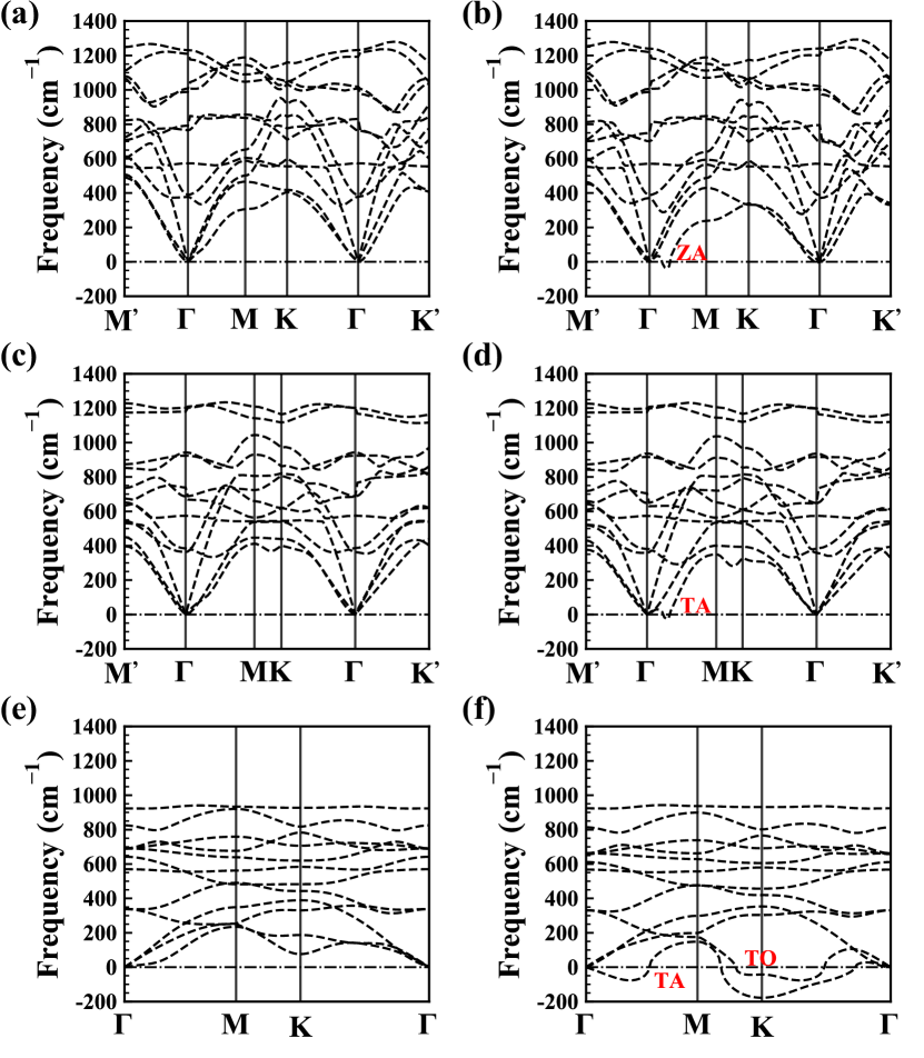
While the stress strain relation provides a rough indication of the ideal strength of CN nanosheet, it is still necessary to check whether the structure stability could be maintained before approaching the maximum stress, because the elastic instability may disrupt the homogeneous lattice structure on the strain path (the instability is not soft mode) [50, 51]. In Fig. 6, we present the anisotropic phonon dispersion curves for CN nanosheet under tensile strain. At uniaxial strain , there is no indication of phonon instability, that is, all of phonon frequencies shown are positive [Fig. 6(a)]. With the increasing of tension, the phonon instability does occur at [Fig. 6(b)]. The eigenvectors of the unstable phonon indicate that this phonon branch is the ZA mode (Fig. S1, supplementary material). Noted that the critical strain is beyond maximum strain which means the ideal strength, GPa, could be attained along armchair direction. In comparison, the phonon dispersion curves maintain stable until the uniaxial strain , but then initially has a negative frequency on the TA phonon branch at . The ideal strength is thus obtained ahead of the maximum strength, i.e., GPa, at . For biaxial tension, the TA branch and TO branch phonon instability simultaneously occur at . It indicates that the failure mechanism under biaxial tension is the combination of the phonon instability and elastic instability.
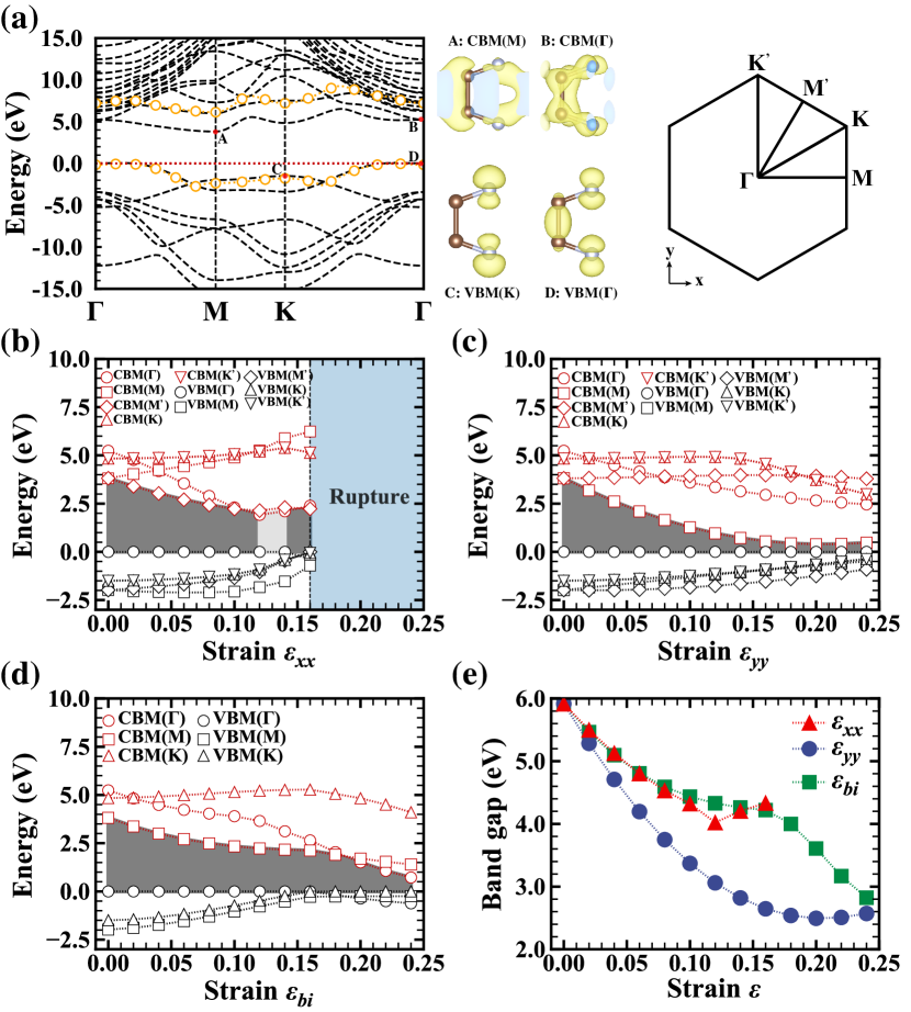
Not only mechanical properties and atomic configuration but also the electronic properties of CN nanosheet, specifically its band gap, can be tailored through stretching. Our results on the electronic band structures of CN nanosheet and its variation with respect to different tensile strains are presented in Fig. 7. As expected, CN nanosheet with covalent interlayer bonding is determined to be semiconductor with an indirect band gap at equilibrium state. It is the fact that all electrons are involved in the formation of covalent bonds in both in-plane and out-of-plane direction. PBE predicts an indirect band gap of 3.8 eV formed from the valance band maximum (VBM) at the point to the conduction band minimum (CBM) at the M point and a direct band gap of 5.2 eV at the point. With corrections, the bands are shifted significantly in energy and the shift is not constant for different bands, resulting in a large increase of band gap at the M point than the point. The band gap corrections at high symmetry points are calculated to be 2.1 eV at point, and 2.6 eV at M and K point. This yields 6.2 eV and 7.3 eV for the indirect and direct transition, respectively. In contrast, regardless of the instability in the out-of-plane direction, the monolayer structures without the interlayer bonding (Fig. 1(c) and Fig. 1(e)) are calculated to display a metallic character (Fig. S2, supplementary material). With this in mind, the CN nanosheet is convinced to be a semiconductor with wide indirect band gap.
The analysis of isosurface charge density could provide a comprehensive understanding of the orbital composition of electronic band. The highest valance state is comprised by atomic orbitals along the perpendicular direction, i.e., strong orbital between C atoms together with partial orbital of N atoms, and the second highest valance state is exclusively composed by partial orbitals perpendicular to atomic plane. For lowest and second lowest conduction band, both the in-plane and out-of-plane atomic orbitals take part in the band formation. Thus, the strong interlayer bonding substantially reshape the band structure and electronic properties of CN nanosheet.
We have plotted the variation of VBM and CBM obtained with PBE as functions of different tensile strains in Fig. 7(b-d). Generally, the band gap decreases with increasing tensile strain in the elastic region for tensile strain and . For armchair tension , the band gap first decreases with increasing armchair tension, passing through a minimum, then increases and forms a direct band gap from to . This direct band gap is a consequence of the intersection of CBM between and . With the increasing of these three tensions, there is tendency that the VBM at other high symmetry points (M, K and their splitting under uniaxial tension) are raised with regard to the VBM at . However, the variations of CBM are much more complicated and shows strong anisotropy to the applied strain. Finally, variations of band gap with respect to the tensile strain are summarized in Fig. 7(e). It is notable that these band gap results are obtained at the PBE level and then corrected using the scissors operator method based on the 2.1 eV difference between the PBE and PBE+ band gap at the point. Accordingly, the electronic band structure of CN nanosheet can be constructively controlled by tensile strain and the transition between direct and indirect band gaps can be realized. Similar trends can be also found for 2D C(=Si, Ge, As) nanosheets in our early work [52]. Thus strained CN nanosheet have important and potential applications in optoelectronics and energy engineering.
IV Conclusion
In summary, we have investigated the elastic, vibrational and electronic properties of the CN nanosheet in the puckered honeycomb structure with covalent interlayer bonding using first-principles simulations. The strong interlayer bonding between C atoms together with the hybrid intralayer bonding of C-N atoms maintain the structure stability of CN nanosheet. It is found that CN nanosheet has an effective Young’s modulus of 1013 GPa which indicates comparable in-plane stiffness to monolayer graphene. A negative Poisson’s ratio in the out-of-plane direction under biaxial deformation, which is attributed to additional degree of atomic relaxation introduced by the interlayer bonding, is revealed. The highly anisotropic mechanical and electronic response of CN nanosheet to the tensile strain have been explored. It is identified that the tensile strength of CN nanosheets are dictated by the instability of out-of-plane transverse phonon branch ZA for armchair tension , but in-plane transverse phonon branch TA for the zigzag tension . Our results show that the band structure of CN nanosheet could be effectively tailored through strain engineering. This work demonstrates that CN nanosheet can be engineered through the controlling of covalent interlayer bonding and applied strain to enhance structure stability, increase buckling strength, and modify band gap, all indispensable characteristics for potential application in the nanoelectromechanical system.
Acknowledgements.
This work is supported by the Special Program for Applied Research on Super Computation of the NSFC-Guangdong Joint Fund (the second phase) under grant no. U1501501, and the Xiamen University Malaysia Research Fund, grant no. XMUMRF/2019-C3/IORI/0001.References
- Novoselov et al. [2004] K. S. Novoselov, A. K. Geim, S. V. Morozov, D. Jiang, Y. Zhang, S. V. Dubonos, I. V. Grigorieva, and A. A. Firsov, Electric field effect in atomically thin carbon films, Science 306, 666 (2004).
- Zhang et al. [2005] Y. Zhang, Y. W. Tan, H. L. Stormer, and P. Kim, Experimental observation of the quantum Hall effect and Berry’s phase in graphene, Nature 438, 201 (2005).
- Berger et al. [2006] C. Berger, Z. Song, X. Li, X. Wu, N. Brown, C. Naud, D. Mayou, T. Li, J. Hass, A. N. Marchenkov, E. H. Conrad, P. N. First, and W. A. de Heer, Electronic confinement and coherence in patterned epitaxial graphene, Science 312, 1191 (2006).
- Nakano et al. [2006] H. Nakano, T. Mitsuoka, M. Harada, K. Horibuchi, H. Nozaki, N. Takahashi, T. Nonaka, Y. Seno, and H. Nakamura, Soft synthesis of single-crystal silicon monolayer sheets, Angew. Chem. Int. Ed. 45, 6303 (2006).
- Cahangirov et al. [2009] S. Cahangirov, M. Topsakal, E. Aktürk, H. Şahin, and S. Ciraci, Two- and one-dimensional honeycomb structures of silicon and germanium, Phys. Rev. Lett. 102, 236804 (2009).
- Wallace [1947] P. R. Wallace, The band theory of graphite, Phys. Rev. 71, 622 (1947).
- Liu et al. [2014] H. Liu, A. T. Neal, Z. Zhu, Z. Luo, X. Xu, D. Tomanek, and P. D. Ye, Phosphorene: an unexplored 2D semiconductor with a high hole mobility, ACS Nano 8, 4033 (2014).
- Li et al. [2014] L. Li, Y. Yu, G. J. Ye, Q. Ge, X. Ou, H. Wu, D. Feng, X. H. Chen, and Y. Zhang, Black phosphorus field-effect transistors, Nat. Nanotechnol. 9, 372 (2014).
- Lin et al. [2015] J.-H. Lin, H. Zhang, and X.-L. Cheng, First-principle study on the optical response of phosphorene, Front. Phys. 10, 1 (2015).
- Zheng et al. [2002] J.-C. Zheng, H.-Q. Wang, A. Wee, and C. Huan, Structural and electronic properties of Al nanowires: an pseudopotential study, Int. J. Nanosci. 1, 159 (2002).
- Wang et al. [2019] Z.-Q. Wang, T.-Y. Lü, H.-Q. Wang, Y. P. Feng, and J.-C. Zheng, Review of borophene and its potential applications, Front. Phys. 14, 33403 (2019).
- Lei et al. [2015] J.-C. Lei, X. Zhang, and Z. Zhou, Recent advances in MXene: Preparation, properties, and applications, Front. Phys. 10, 276 (2015).
- Niu et al. [1993] C. Niu, Y. Z. Lu, and C. M. Lieber, Experimental realization of the covalent solid carbon nitride, Science 261, 334 (1993).
- Yu et al. [1994] K. M. Yu, M. L. Cohen, E. E. Haller, W. L. Hansen, A. Y. Liu, and I. C. Wu, Observation of crystalline , Phys. Rev. B 49, 5034 (1994).
- Song et al. [1994] H. W. Song, F. Z. Cui, X. M. He, W. Z. Li, and H. D. Li, Carbon nitride films synthesized by -ion-beam-assisted deposition, J. Phys. Condens. Matter 6, 6125 (1994).
- Bousetta et al. [1994] A. Bousetta, M. Lu, A. Bensaoula, and A. Schultz, Formation of carbon nitride films on Si(100) substrates by electron cyclotron resonance plasma assisted vapor deposition, Appl. Phys. Lett. 65, 696 (1994).
- Zhang et al. [1995] Z. J. Zhang, S. Fan, and C. M. Lieber, Growth and composition of covalent carbon nitride solids, Appl. Phys. Lett. 66, 3582 (1995).
- Pearce et al. [2002] S. R. J. Pearce, P. W. May, R. K. Wild, K. R. Hallam, and P. J. Heard, Deposition and properties of amorphous carbon phosphide films, Diam. Relat. Mater. 11, 1041 (2002).
- Claeyssens et al. [2004] F. Claeyssens, G. M. Fuge, N. L. Allan, P. W. May, and M. N. R. Ashfold, Phosphorus carbides: theory and experiment, Dalton Trans. , 3085 (2004).
- Hart et al. [2013] J. N. Hart, P. W. May, N. L. Allan, K. R. Hallam, F. Claeyssens, G. M. Fuge, M. Ruda, and P. J. Heard, Towards new binary compounds: Synthesis of amorphous phosphorus carbide by pulsed laser deposition, J. Solid State Chem. 198, 466 (2013).
- Furlan et al. [2008] A. Furlan, G. K. Gueorguiev, Z. Czigány, H. Högberg, S. Braun, S. Stafström, and L. Hultman, Synthesis of phosphorus-carbide thin films by magnetron sputtering, Phys. Status Solidi RRL 2, 191 (2008).
- Côté and Cohen [1997] M. Côté and M. L. Cohen, Carbon nitride compounds with 1:1 stoichiometry, Phys. Rev. B 55, 5684 (1997).
- Zheng et al. [2003] J.-C. Zheng, M. C. Payne, Y. P. Feng, and A. T.-L. Lim, Stability and electronic properties of carbon phosphide compounds with 1:1 stoichiometry, Phys. Rev. B 67, 153105 (2003).
- Wang et al. [2016] G. Wang, R. Pandey, and S. P. Karna, Carbon phosphide monolayers with superior carrier mobility, Nanoscale 8, 8819 (2016).
- Geim and Grigorieva [2013] A. K. Geim and I. V. Grigorieva, Van der Waals heterostructures, Nature 499, 419 (2013).
- Novoselov et al. [2016] K. S. Novoselov, A. Mishchenko, A. Carvalho, and A. H. Castro Neto, 2D materials and Van der Waals heterostructures, Science 353, aac9439 (2016).
- Hu et al. [2017] X.-R. Hu, J.-M. Zheng, and Z.-Y. Ren, Strong interlayer coupling in phosphorene/graphene Van der Waals heterostructure: A first-principles investigation, Front. Phys. 13, 137302 (2017).
- de Andres et al. [2008] P. L. de Andres, R. Ramírez, and J. A. Vergés, Strong covalent bonding between two graphene layers, Phys. Rev. B 77, 045403 (2008).
- Li et al. [2021] J.-J. Li, Y. Dai, and J.-C. Zheng, Strain engineering of ion migration in , Front. Phys. 17, https://doi.org/10.1007/s11467-021-1086-5 (2021).
- Kanasaki et al. [2009] J. Kanasaki, E. Inami, K. Tanimura, H. Ohnishi, and K. Nasu, Formation of -bonded carbon nanostructures by femtosecond laser excitation of graphite, Phys. Rev. Lett. 102, 087402 (2009).
- Nishioka and Nasu [2010] K. Nishioka and K. Nasu, Cooperative domain-type interlayer -bond formation in graphite, Phys. Rev. B 82, 035440 (2010).
- Ghosh et al. [2010] S. Ghosh, W. Bao, D. L. Nika, S. Subrina, E. P. Pokatilov, C. N. Lau, and A. A. Balandin, Dimensional crossover of thermal transport in few-layer graphene, Nat. Mater. 9, 555 (2010).
- Wei et al. [2011] Z. Wei, Z. Ni, K. Bi, M. Chen, and Y. Chen, In-plane lattice thermal conductivities of multilayer graphene films, Carbon 49, 2653 (2011).
- Guo et al. [2015] T. Guo, Z.-D. Sha, X. Liu, G. Zhang, T. Guo, Q.-X. Pei, and Y.-W. Zhang, Tuning the thermal conductivity of multi-layer graphene with interlayer bonding and tensile strain, Appl. Phys. A 120, 1275 (2015).
- Giannozzi et al. [2009] P. Giannozzi, S. Baroni, N. Bonini, M. Calandra, R. Car, C. Cavazzoni, D. Ceresoli, G. L. Chiarotti, M. Cococcioni, I. Dabo, A. D. Corso, S. de Gironcoli, S. Fabris, G. Fratesi, R. Gebauer, U. Gerstmann, C. Gougoussis, A. Kokalj, M. Lazzeri, L. Martin-Samos, N. Marzari, F. Mauri, R. Mazzarello, S. Paolini, A. Pasquarello, L. Paulatto, C. Sbraccia, S. Scandolo, G. Sclauzero, A. P. Seitsonen, A. Smogunov, P. Umari, and R. M. Wentzcovitch, QUANTUM ESPRESSO: a modular and open-source software project for quantum simulations of materials, J. Phys. Condens. Matter 21, 395502 (2009).
- Perdew et al. [1996] J. P. Perdew, K. Burke, and M. Ernzerhof, Generalized gradient approximation made simple, Phys. Rev. Lett. 77, 3865 (1996).
- Blöchl [1994] P. E. Blöchl, Projector augmented-wave method, Phys. Rev. B 50, 17953 (1994).
- Levine and Allan [1989] Z. H. Levine and D. C. Allan, Linear optical response in silicon and germanium including self-energy effects, Phys. Rev. Lett. 63, 1719 (1989).
- Fiorentini and Baldereschi [1995] V. Fiorentini and A. Baldereschi, Dielectric scaling of the self-energy scissor operator in semiconductors and insulators, Phys. Rev. B 51, 17196 (1995).
- Hybertsen and Louie [1986] M. S. Hybertsen and S. G. Louie, Electron correlation in semiconductors and insulators: Band gaps and quasiparticle energies, Phys. Rev. B 34, 5390 (1986).
- Zakharov et al. [1994] O. Zakharov, A. Rubio, X. Blase, M. L. Cohen, and S. G. Louie, Quasiparticle band structures of six II-VI compounds: ZnS, ZnSe, ZnTe, CdS, CdSe, and CdTe, Phys. Rev. B 50, 10780 (1994).
- Trevisanutto et al. [2008] P. E. Trevisanutto, C. Giorgetti, L. Reining, M. Ladisa, and V. Olevano, many-body effects in graphene, Phys. Rev. Lett. 101, 226405 (2008).
- Şahin et al. [2009] H. Şahin, S. Cahangirov, M. Topsakal, E. Bekaroglu, E. Akturk, R. T. Senger, and S. Ciraci, Monolayer honeycomb structures of group-IV elements and III-V binary compounds: First-principles calculations, Phys. Rev. B 80, 155453 (2009).
- Lee et al. [2008] C. Lee, X. Wei, J. W. Kysar, and J. Hone, Measurement of the elastic properties and intrinsic strength of monolayer graphene, Science 321, 385 (2008).
- Jiang [2015] J.-W. Jiang, Graphene versus : A short review, Front. Phys. 10, 287 (2015).
- Liu et al. [2007] F. Liu, P. Ming, and J. Li, calculation of ideal strength and phonon instability of graphene under tension, Phys. Rev. B 76, 064120 (2007).
- Wu et al. [2013] J. Wu, B. Wang, Y. Wei, R. Yang, and M. Dresselhaus, Mechanics and mechanically tunable band gap in single-layer hexagonal boron-nitride, Mater. Res. Lett. 1, 200 (2013).
- Jiang et al. [2016] J.-W. Jiang, T. Chang, X. Guo, and H. S. Park, Intrinsic negative Poisson’s ratio for single-layer graphene, Nano Lett. 16, 5286 (2016).
- Qin and Qin [2020] G. Qin and Z. Qin, Negative Poisson’s ratio in two-dimensional honeycomb structures, Npj Comput. Mater. 6, 51 (2020).
- Li et al. [2007] T. Li, J. W. Morris, N. Nagasako, S. Kuramoto, and D. C. Chrzan, “ideal” engineering alloys, Phys. Rev. Lett. 98, 105503 (2007).
- Li [2012] T. Li, Ideal strength and phonon instability in single-layer MoS2, Phys. Rev. B 85, 235407 (2012).
- Lü et al. [2012] T.-Y. Lü, X.-X. Liao, H.-Q. Wang, and J.-C. Zheng, Tuning the indirect–direct band gap transition of SiC, GeC and SnC monolayer in a graphene-like honeycomb structure by strain engineering: a quasiparticle study, J. Mater. Chem. 22, 10062 (2012).