Carrier concentrations and optical conductivity of a band-inverted semimetal in two and three dimensions
Abstract
Here we study the single-particle, electronic transport and optical properties of a gapped system described by a simple two-band Hamiltonian with inverted valence bands. We analyze its properties in the three-dimensional (3D) and the two-dimensional (2D) case. The insulating phase changes into a metallic phase when the band gap is set to zero. The metallic phase in the 3D case is characterized by a nodal surface. This nodal surface is equivalent to a nodal ring in two dimensions. Within a simple theoretical framework, we calculate the density of state, the total and effective charge carrier concentration, the Hall concentration and the Hall coefficient, for both 2D and 3D cases. The main result is that the three concentrations always differ from one another in the present model. These concentrations can then be used to resolve the nature of the electronic ground state. Similarly, the optical conductivity is calculated and discussed for the insulating phase. We show that there are no optical excitations in the metallic phase. Finally, we compare the calculated optical conductivity with the rule-of-thumb derivation using the joint density of states.
I Introduction
The topological quest within the solid state physics is to identify properties that originate from the so called non trivial topology of the Bloch bands Hasan and Kane (2010); Xiao et al. (2010). Many systems have been explored. Most familiar are the Dirac and Weyl semimetals, which contain a whole array of candidate materials Armitage et al. (2018). Their common underlying feature is that the valence and conduction bands touch in one or more isolated points in the Brillouin zone Polatkan et al. (2020); Habibi et al. (2021); Ahn et al. (2017). A natural extension of the band point-touch is a band line-touch. Such materials are known as nodal-line semimetals Carbotte (2016); Rhim and Kim (2016); Shao et al. (2019). Analogously, extending the idea of the nodal line semimetal leads to the nodal surface semimetal (NSSM), in which the bands touch over a surface spanned in the Brillouin zone Wang et al. (2018). This surface is equivalent to a line in the 2D case Jin et al. (2020).
In this article, we address the simplest case of NSSM in 3D and 2D. We also explore their gapped phase, which we refer to as the gapped semimetal phase (GSM). We analyze the single-particle intraband and interband properties of the system described by a two-band Hamiltonian. The Hamiltonian contains three free parameters and it describes the gapped (GSM) and the metallic (NSSM) phase. The energy bands’ main feature is the inverted shape up to some critical energy McCann (2006); Guinea et al. (2006) and a parabolic free-electron-like dispersion at energies beyond the band inversion. Our intention is twofold. First, we want to answer the question: Can the experiments such as the electronic transport and optical measurements resolve the two possible ground states, gapped (GSM) and semimetallic (NSSM)? This tackles the main problem inherent to nearly all topological materials. Their intrinsic energy scales—energy intervals within the Bloch bands—where their topological properties can be observed is small, often not more than several milli-electron-volts. This makes it challenging to experimentally distinguish between different possible ground states.
Second, we want to show how the DC and optical properties differ in the 3D and 2D cases of such semimetals. The DC quantities include the density of state per unit volume, the total and the effective concentration of the charge carriers, the Hall concentration and the Hall coefficient. We show that very generally those concentrations differ for both GSM and NSSM phases, in 2D and in 3D. Therefore, by comparing the Drude weight and the Hall concentration with the total concentration, we can determine the nature of the ground state. The discrepancies between the GSM and NSSM phases are even more evident in the optical conductivity. The NSSM phase has no optical excitations since the amplitude of the interband current matrix element is proportional to the energy gap . In the GSM case, we calculate the real part of the optical conductivity within the vanishing and finite interband relaxation constant approximation.
Without interband relaxation, the optical conductivity has the same shape for 3D and 2D when incident photon energy is just above the band gap. It has a square-root singularity . For large energies, the conductivity scales with the dimension as .
Knowing the specific Bloch momentum dependence of the interband current vertex, we show when one can use the joint density of state rule-of-thumb calculation Dressel and Grüner (2002) to estimate the real part of the optical conductivity.
This paper is structured as follows: In the first part of the article we specify the model Hamiltonian for the GSM and NSSM phase. We then define and calculate for the 3D case the density of states, the three concentrations of charge carriers (total, effective and Hall) and the real part of the optical conductivity. Finally, we calculate all these quantities for the 2D case.
II Two-band Hamiltonian
As a starting point, we define a continuum isotropic Hamiltonian matrix that describes the general form of GSM and consequently the NSSM phase Pal et al. (2016); Zhang et al. (2016); Carrington (2011). The Hamiltonian is
| (2.1) |
where and are the Pauli matrices and and are positive constants representing the gap parameters. The is the “inverted part”. It is the simplest isotropic form of a nodal surface, with being the square of the total Bloch wave vector. The positive parameter can be written in a more familiar way as . The effective mass will come in handy when the DC properties are discussed in the next section. The Hamiltonian (2.1) is invariant under spatial inversion, and since it is a real matrix it is also invariant under time reversal. The latter also implies vanishing Berry curvature Gradhand et al. (2012); Sinitsyn et al. (2007) making this system topologically trivial. This Hamiltonian is a simplified variant of the Bernevig–Hughes–Zhang Hamiltonian Bernevig et al. (2006); Peres and Santos (2013), with a constant electron-hole coupling described by the parameter .
The diagonalization of Eq. (2.1) is straightforward. It gives an electron-hole symmetric eigenvalues
| (2.2) |
The indices and stand for conduction band (plus sign) and valence band (minus sign), respectively.
To make the analysis of the electron properties originating from Eq. (2.1) as general as possible, we scale the eigenvalues Eq. (2.2) to the gap parameter and introduce dimensionless substitutions. These substitutions are a dimensionless gap and a dimensionless wave vector . In this way, the eigenvalues above become much simpler:
| (2.3) |
with the definition .
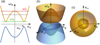
The dispersions given by Eq. (2.3) are shown in Fig. 1. Bands for the 1D and 2D case are shown, together with the Fermi surface in 3D. The height of the band inversion is described by the parameter , while gives the minimum band separation. In dimensionless units this differentiates the two phases, GSM and NSSM. From Eq. (2.3) for GSM we have , and for NSSM . In the three-dimensional NSSM case the two bands touch along the spherical surface of radius . The sphere becomes a circle in 2D. In 1D case we can depict in Fig. 1a, as the distance between the two points where the bands touch.
If the value of the Fermi energy is restricted to , the Fermi surface consists of two concentric spheres in 3D or concentric circles in 2D. With
| (2.4) |
we designate the energy belonging to the bottom () and the top () of the inverted band as shown in Fig. 1(a) and (b). Energies (2.4) to a great extent determine the specific behavior of the DC concentrations and the optical response, as it will be shown in the following sections. These energies, and , define the energy interval where the inverted bands directly influence the electronic transport.
III 3D case
III.1 Density of states
Here we derive the density of states (DOS) per unit volume for the energy dispersion Eq. (2.2). The calculation is performed for the 3D case. The same procedure is applied for the 2D case later on (Sec. VI). By definition, the DOS per unit volume is
| (3.1) |
We use the dimensionless variables defined in the previous section for carrying out the calculation. We change the sum in Eq. (3.1) into integral in spherical coordinates
| (3.2) |
The delta function in Eq. (3.2) is evaluated by decomposing it into a sum
| (3.3) |
where are the positive zeros of the function argument
| (3.4) |
written with the help of a substitution , defined in Eq. (2.4). Inserting Eq. (3.3) back into Eq. (3.2), we obtain almost the final expression for DOS in 3D
| (3.5) |
To make zeros real, the sub-root function in Eq. (3.4) has to be positive. This depends on the value of . It is easy to check that if , then both and are real, since the sub-root expression always remains positive. On the other hand, for only is real. All of these restrictions on the allowed intervals of and on the sum over any function of , can be encoded into with the help of the Heaviside step function
| (3.6) |
Using the recipe Eq. (III.1) on Eq. (3.5) we obtain the final result for the 3D DOS, which after some trivial rearrangement of the step functions is
| (3.7) |
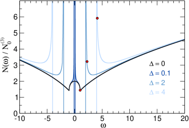
Equation (III.1) is plotted in Fig. 2 for different values of the parameter in the units of . In the NSSM case , Eq. (III.1) gives the DOS with a dome-like shape between the points , as seen from definition (2.4). For a finite value of we obtain the GSM case where DOS has a square root singularity at . Expanding Eq. (III.1), we get
| (3.8) |
Fig. 2 also shows the value of designated by the red circles. This shows how fast as we increase . While determines the DOS onset, nothing spectacular happens at . In the high energy limit we obtain the same DOS as for the 3D free electron gas.
IV The DC transport quantities in 3D
There are three concentrations of the charge carriers, for example electrons, usually associated with the DC transport. These are the total concentration , the effective concentration , and the Hall concentration . All the three concentrations are functions of the Fermi energy .
In the trivial case of a free electron gas, these three concentrations are identical. As soon as the dispersion becomes more complex, they begin to deviate from one another. This is because these charge concentrations are each associated with a different transport concept. The simplest of them is a measure of the total charge added into the system, , and it is temperature-independent. The second and the third one, and , are temperature-dependent. However, in the limit, we can give each of them a simple interpretation. In that limit, becomes the average electron kinetic energy at the Fermi level. Physically, from the classical Hall experiment, one measures the ratio of transversal voltage and longitudinal current, in the limit of a vanishing magnetic field. This ratio is called the Hall coefficient, , and has the dimension of inverse concentration. Only in the simplest version—parabolic free electron dispersion—can we trivially connect with the total carrier concentration. For any more complex band dispersion, can only be calculated through semiclassical Boltzmann transport equations, and the resulting concentration is called the Hall concentration .
IV.1 Total charge carrier concentration
The total carrier concentration is accessible immediately from the DOS. Using the integral representation we have
| (4.1) |
The total concentration of the intrinsic system can be controlled by chemical doping or through electrostatic doping. Inserting Eq. (III.1) in the above expression we obtain
where we have introduced a constant for this 3D case
| (4.3) |
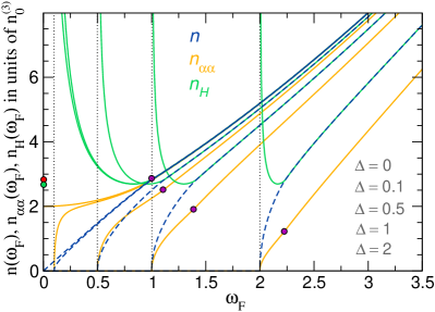
The total concentration is plotted in Fig. 3 (blue dashed line) for several values of the parameter . To show some of the properties of as a function of the Fermi level , Eg. (IV.1) is approximated in several interesting limits of :
| (4.4) |
The concentration which corresponds to the filling of the band up to the top of the inverted parabola is and is indicated in the Fig. 3 by the red circle.
IV.2 Effective charge carrier concentration
The effective concentration defines the Drude weight. It is a spatially dependent quantity, which at is given by Mahan (2000); Rukelj et al. (2020)
| (4.5) |
Here is a Cartesian component, is the bare electron mass and is the electron group velocity. The derivative of Eq. (2.2) is taken over (the remaining spatial components give the same result), and inserted in to Eq. (4.5). The summation is changed into integration over the dimensionless variables and . The evaluation of Eq. (4.5) is similar to the procedure outlined in the previous subsection. The result is
In writing Eq. (IV.2) we used the definition of the effective mass from the Sec. II. The resulting expression is relatively similar to Eq. (IV.1). Apart from the and the additional prefactor, there is also a sign difference within the brackets. Comparison of and is shown in Fig. 3. The differences and similarities between the two carrier concentrations are most noticeable in the following limits:
| (4.7) |
Within the energy range the difference between the and the gives a fingerprint of the NSSM phase. The former has a linear–like dependence on the Fermi energy while the later is nearly constant. The GSM phase is characterized by for just above . However, there is a subtle difference between the square root amplitude of the two concentrations. From Fig. 3 we see a large square root amplitude in , while is nearly a straight line for small . This behavior is flipped for bigger . The value of the effective concentration at the band peak is diminishing as we increase . This is seen by the position of the violet circles in Fig. 3. In the high energy limit , the bands (2.2) are free-electron-like with the effective mass . In this limit we recover a well known property Rukelj (2020).
IV.3 Hall concentration and coefficient
Hall concentration of conducting electrons has a fundamental role in the transport equations in the presence of a weak external magnetic field. changes sign at the energies where the electrons make way for holes as the dominant charge carriers. This can be accomplished either by doping Badoux et al. (2016); Zhu et al. (2009) or by changing the temperature Martino et al. (2019); LeBoeuf et al. (2007). The exact derivation of from the semi-classical transport equations is rather complicated and can be found in Samanta et al. (2021); Kupčić and Jedovnicki (2017); Ong (1991); C. and Jones H. (1934). Here we only recall the limiting low-field value of for a magnetic field pointing in direction and when :
| (4.8) |
where the concentrations and are given by Eq. (4.5). For our specific model, we have from Eq. (IV.2), while is defined as
| (4.9) |
is a reciprocal effective mass tensor
| (4.10) |
The Hall coefficient is where is the charge of an electron. Taking the first and second derivatives of the dispersion Eq. (2.2) it is straightforward to show, Appendix A, that
| (4.11) |
After a direct evaluation of Eq. (4.11) by the procedure outlined in Sec. III.1 and as shown in Appendix A, we obtain an interesting result:
| (4.12) |
Now we have all the ingredients to calculate the Hall concentration from Eq. (4.8):
| (4.13) |
as a function of Fermi energy is shown in Fig. 3 (green line) for several values of the parameter . To clarify the main features of we expand Eq. (IV.3) for specific limits of as we did in the case of and :
| (4.14) |
As seen from Fig. 3, unlike and , is not a monotonic function of . It diverges in both NSSM and GSM phases when is zero or just above the bottom energy . Then as is increased it drops to a minimal value only to continue to grow again. The energy which corresponds to the minimum of is determined by equating the first derivative of Eq. (IV.3) to zero. This can be done analytically and it gives , where . Correspondingly , a value designated by the green circle on the axes in Fig. 3. Clearly, the energy range in which decreases and exhibits a minimum is within the range and is associated with the inverted part of the conduction band. Above , is equal to the total concentration and increases with .
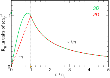
Usually the Hall coefficient is expressed as a function of total concentration . To do so, we invert the Eq. (IV.1) and find as function of . We then insert into Eq. (IV.3). For the 3D case, this procedure is done numerically, yielding and consequently shown in Fig. 4 in green. is plotted as a function of scaled concentration where, as noted before . If the concentration is small enough, then we have . Above , . The maximum of is located at the same point as the minimum of . In scaled units this point is located at , and gives the height of the peak as indicated by the green circle in Fig. 4. This shows again that Hall coefficient is a function of total electron concentration, above the critical doping , just as we expect it should be for a free electron gas. However, below this critical concentration, it has an unexpected linear-like decrease.
Finally, Eq. (IV.3) applies only at . For finite temperatures the Fermi-Dirac distribution derivative replaces the delta function. This alters the end result, because of the temperature dependence of the electron chemical potential.
The results in this Section clearly show that in this system all three carrier concentrations are mutually different. The intrinsic NSSM case is characterised by a zero value of , a constant value of and a diverging . The intrinsic GSM phase, on the on the other hand, has a zero value of and , while diverges again. This difference between the concentrations is even more evident once we step down a dimension, moving from 3D to 2D.
V Optical conductivity
V.1 General optical conductivity formula
In a two-band model we can write the complex interband conductivity tensor Kupčić et al. (2013); Rukelj et al. (2020)
| (5.1) |
where is a phenomenological interband relaxation rate, and the Cartesian component of the interband conductivity tensor is a function of the incident photon energy . In Eq. (5.1) the -dependent interband current vertices are calculated from the Hamiltonian (2.1) in Appendix B. We analytically evaluate the real part of the conductivity tensor (5.1) in the limit for the two band model Eq. (2.1). The result is
The Fermi-Dirac distributions in the above expression are simplified by taking into account the symmetry of the bands and the fact that the expression Eq. (V.1) is finite only for . We define
| (5.3) |
In the case, the above expression simplifies to , which describes the suppression of the interband transitions due to the Pauli blocking. Finally we arrive at a simple expression for the real part of the optical conductivity
| (5.4) |
V.2 Optical conductivity of the 3D case
We now calculate the real part of the interband conductivity defined from expression Eq. (5.4). The interband current vertex is derived in Appendix B and it is
| (5.5) |
In our model, is a real quantity proportional to the band gap parameter. By inspecting the Hamiltonian (2.1) we see that by setting the off-diagonal elements () to zero, there is nothing that could induce the transition between the diagonal elements. Here this is demonstrated by the shape of which states the same thing. We conclude that in the NSSM phase there are no optical excitations.
In the GSM phase, we insert the current vertex Eq. (5.5) into Eq. (5.4) and change the summation to the integral as we did in the Sec. III.1. Once again, we make use of the dimensionless variables and which we now define as . With this choice of scaling, and become equal. This is best seen by looking at the delta function argument within the integral form of the conductivity in Eq. (5.4)
| (5.6) |
The aforementioned substitutions enable us to retain the energy scales and , which we had defined in the Sec. II, and which are for this purpose renamed to and . The conductivity constant has been defined in the previous expression . Omitting the index in the conductivity from now on, the function in Eq. (V.2) is solved by a decomposition into a sum of zeros Eq. (3.4). Using the recipe (III.1) we get
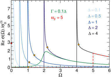
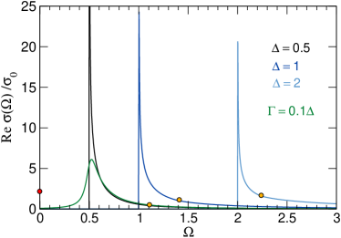
Conductivity Eq. (V.2) is shown for the GSM case in Fig. 5 for several values of the gap parameter in units of . From the expression Eq. (V.2) we immediately see that the amplitude of depends on the gap value , which implies that the optical conductivity vanishes in the NSSM case as stated earlier. However, the most striking feature is the divergence of at the energy . This divergence is of the square-root type as it can be seen from the expansion of Eq. (V.2) for just above :
| (5.8) |
The divergence in the optical response for the energy is seen only in the intrinsic case, when the Fermi energy is zero and . As soon as the doping becomes finite, the Pauli blockade removes this divergence from the interval of accessible excitation energies (red dashed line in Fig. 5). In the intrinsic case of a simple 3D Schrödinger-like direct-gap insulator, the onset of the optical transitions is connected with a transition between two points Cardona and Peter (2010). These two points are the top of the valence band and the bottom of the conduction band. The onset of the optical transitions of the GSM case is characterized by the excitations of the entire surface of points from to . This leads to the divergent response in the optical conductivity. The “amplitude” of the divergence in the real part of the conductivity is also governed by . The lower this energy is, the more profound the singularity, as seen from Eq. (V.2) and as shown in Fig. 5 from comparing the blue curves of different shades.
A finite doping removes the divergence in the optical spectrum. Similarly, this divergence is lifted by taking a finite interband relaxation in the calculation of . This leads to the removal of the singularity since at the we have . For even larger values of , the optical response of the intrinsic case is entirely smeared, as seen in Fig. 5.
On the other hand, the high limit is proportional to and dies off quickly as we lower the value of , see Fig 5. The upper dome energy bears no significance in . Its position is depicted by the orange circles in Fig. 5. The limiting value of these orange circles approaches (shown by the red circle) when increases. The distance between and determines the width of the conductivity peak which is located between these two points. From the definition of and in Eq. (2.4), it is evident that the width decreases with increasing . A final note about Eq. (V.2): the optical conductivity as a function of the photon energy and the three parameters of the Hamiltonian (2.1) and can be easily obtained. In Eq. (V.2) we simply need to change and .
VI 2D case
VI.1 DOS and the charge concentrations
Eq. (V.2)
So far, we have described the single-particle transport and optical properties of the 3D GSM and NSSM phases. In this section we repeat a similar analysis for the two dimensional version of the system described in Sec. II. Hence, the main difference is the dimension of the integral which needs to be evaluated for various quantities. We start with writing the end result for DOS
| (6.1) |
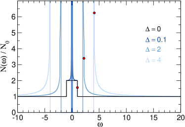
where a helpful variable has been introduced. The DOS in Eq. (6.1) is shown in Fig. 6. The differences are apparent, when compared to its 3D analog in Fig. 2. For the NSSM case a round dome is replaced by a step-like structure spanning between . It has an amplitude of within the interval and the height of outside these boundaries. The finite gap in the GSM phase, like in its 3D analog, introduces a square-root divergence at Nicol and Carbotte (2008). The DOS for the NSSM case is consistent with the result obtained in Barati and Abedinpour (2017).
The total concentration is given as a function of the Fermi energy for the electron-doped case . It follows from Eq. (4.1) with DOS given by Eq. (6.1):
Once again we introduced a useful constant for 2D concentration . The total concentration is shown in Fig. 7a as a dashed blue line. In the NSSM case as inherited from the DOS, below and above but with different slopes. At this specific energy, which in the GSM case corresponds to , the concentration has a value of and a kink in its first derivative over .
The effective concentration follows in the same way as in Sec. IV.2. After inserting the electron velocities in the Eq. (4.5) and changing it into a 2D integral, we obtain
In the NSSM case, has a constant value up to and a linear dependence above , as seen from Fig. 7a where it is depicted with an orange line. The discrepancies between and remain visible over the whole range of values of gap parameter . For small values of just above the , has a square-root dependence on , while in the high energy limit it goes linearly with .
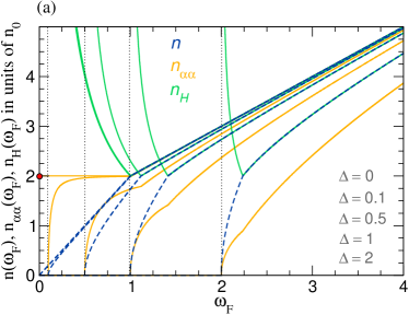
The final concentration to consider is Hall concentration . Since there is a small subtlety in the derivation procedure, we detail it in the Appendix A using the recipe from Sec. IV.3. It leads to:
| (6.4) |
Here is drawn as a green line in Fig. 7a, and it has a dependence below . Equivalently, it has a square-root type of divergence as a function of when (dotted vertical lines). On the other hand, for , it is equal to . Furthermore, inverting Eq. (VI.1) to get and inserting it in Eq. (VI.1) we derive the Hall coefficient as a function of :
| (6.5) |
is the total concentration of electrons when the conduction band is filled to the top of the dome of the inverted band (). Although not in a simple fashion like (6.5), by the same procedure too can be written as a function of :
| (6.6) |
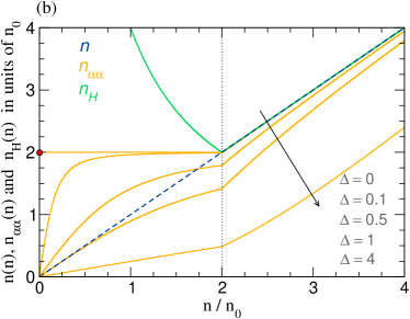
The dependence of and on is depicted in Fig. 7b. The three concentrations of the 2D system differ from one another for energies , or for total concentration . The differentiation between the two ground states NSSM and GSM phase now becomes easy to make. By carefully changing the doping and reading out the Drude weight (), one should obtain a constant in the NSSM phase for . Another valid fingerprint of the band structure (2.1) in the 2D transport is the , which diverges as for . Unlike in the 3D case, the minimum value of is now located at the energy .
In the highly doped limit, where the Fermi energy overshoots the top of the dome , or equivalently where , we expect all the three concentrations to be roughly the same, . This is to be expected since the energy dispersion (2.2) high above the dome is free-electron-like. From Eq. (6.5) we see this is true for and for GSM and NSSM cases. But in this doping regime, only in the NSSM phase, while in the GSM phase it approaches asymptotically as the doping increases.
The Hall coefficient as a function of is reciprocal to Eq. (6.5):
| (6.7) |
and it is shown in Fig. 4 (red dashed line) as a function of , in units of . As in the 3D case, grows linearly with until it reaches a sharp maximum at with a height of . Beyond this maximum, has the same dependence like its 3D analog. Previously, we could find the 3D only numerically. Fortunately, in the 2D case, we can obtain an analytical result for ,. This is why the two-dimensional case provides a valuable insight into the signature of the inverted bands in the magneto-transport Zhu et al. (2009).
VI.2 Optical conductivity of the 2D system
We obtain the integral expression for the 2D GSM optical conductivity by inserting the interband current vertex Eq. (5.5) in the real part of the interband conductivity formula Eq. (5.4). In units of and dimensionless , it reads
Evaluating the above integral in the same way as in Sec. III, we get
As in the 3D case, we can make use of the conductivity constant . For a simple expression like (VI.2), two limiting regimes in are easily found:
| (6.10) |
The conductivity Eq. (VI.2) is plotted in Fig. 8 in units of for several values of the gap parameter in the intrinsic case, . The high energy tail decreases stronger than in 3D, apart from the root-like divergence near the gap energy, which has the same shape as in the 3D case. Such a weak response would be difficult to set apart from the background, if multiple bands are present as they usually are in real systems. is indicated by orange dots and it approaches the red dot as . The impact of the finite interband relaxation on the is depicted in Fig. 8 with a green line.
VII and the JDOS argument
Usually in a system with linear band dispersion the shape of the interband conductivity can be be determined by the rule-of-thumb argument involving the joint density of state (JDOS) Dressel and Grüner (2002). To show how this works, we look at the Eq. (5.4) in the general two-band case
| (7.1) |
If we assume that the interband current vertex does not depend explicitly on , and that , then can be taken outside the sum in Eq. (7.1). The remaining sum over the function is the definition of JDOS. If the bands have electron-hole symmetry, JDOS is equivalent to DOS such that Eq. (7.1) becomes
| (7.2) |
where we have used the definition of DOS (3.1). For the 3D and 2D Dirac systems Ashby and Carbotte (2014); Kupčić (2015) where is the Dirac velocity and hence (7.2) applies.
For the model studied in this article, the JDOS approach does not apply for small photon energies . It is only in the high-energy limit that the Eq. (7.2) can be safely applied. The obvious reason for this is the strong dependence of the current vertex (5.5). A way around it is to notice that in the high energy limit () the dispersion Eq. (2.2) is parabolic, , and isotropic. Also in this limit the inverse function is single valued, which is not the case when , see Sec. III. Hence in dimensions the mean square of the component is and the square of the D-dimensional interband current vertex is
| (7.3) |
where we have used . Inserting (7.3) into Eq. (7.2) we get the same expressions, once we change , as we did for the high- expansion in 2D Eq. (VI.2) and 3D Eq. (V.2).
This line of reasoning for the JDOS rule-of-thumb is not new and can be demonstrated on the example of the massive 2D Dirac system, where, if we designate the band-gap by , we have Jafari (2012). Since the DOS of the massive 2D Dirac system is linear in , in this case Eq. (7.2) gives an exact result for the optical conductivity.
VIII Conclusions
We have addressed the static and dynamic transport properties of the nodal surface semimetals and their gapped phase. The properties of these systems in three and two dimensions are described by the two-band model of the valence electrons. The main feature of this model is the inversion of the valence bands below the certain energy and parabolic like shape for energies above it. The main question we answer is: Can we determine the electronic ground state, GSM or NSSM, by comparing the experimental and the calculated transport and optical properties?
The band inversion is responsible for a specific shape of the NSSM density of state. In the 3D case it is a dome-like structure, while in the 2D case it has a step-like feature. In the GSM phase a square-root divergence occurs in the DOS at the band gap energies.
We have studied three different concentrations of the charge carriers. These are the total, effective and Hall concentration. We have shown that by controlling the doping and comparing the three concentrations we can conclude if the ground state is gapped or not. This is due to the fact that both in 3D and in 2D these three concentrations differ from one another. Only for high doping (Fermi energy much larger than the band gap) do they become equal. The differences between the transport properties are more profound in 2D than in the 3D case. Still, the Hall coefficient shows remarkable similarities between the 3D and 2D when plotted as a function of total concentration.
The optical properties give a definitive proof of the ground state. There are no optical excitations in the NSSM phase, since the conductivity amplitude is proportional to the band gap. The optical response of the GSM phase has a square root divergence above the band gap threshold for both 3D and 2D with a tail dependence in the 2D and a tail in the 3D case.
Finally, the JDOS rule-of-thumb derivation of the optical conductivity is elaborated in detail. For the GSM phase it is shown to work only in the high-energy limit.
IX Acknowledgments
Z. R. acknowledges the hospitality of the University of Fribourg. A. A. acknowledges funding from the Swiss National Science Foundation through project PP00P2_170544.
Appendix A 3D and 2D
The electron velocities for components are
| (1.1) |
The mass tensor components Eq. (4.10) are
| (1.2) |
and
| (1.3) |
The velocity and mass tensor product within Eq. (4.9) is
| (1.4) |
First the 3D case is solved. (1.4) is inserted in Eq. (4.9) and the sum converted to integral with dimensionless variables. This integral contains the function which again is decomposed as
| (1.5) |
The zeros as defined in Sec. III are carefully implemented in (1.5) with particular care on the sign of . This sign is preserved once taken to the power of 3. We get
| (1.6) |
or after we rearrange the functions
Comparing (A) with Eq. IV.1 we conclude
| (1.8) |
In deriving Eq. (A) we have used the definition of constant (4.3)
| (1.9) |
as well as . Finally the Hall concentration follows from the definition as written in main text.
The same procedure applies for the 2D case. First we reorganise the functions within the effective concentration Eq. (VI.1)
| (1.10) |
Next we calculate using Eq. (4.9) and Eq. (1.4)
| (1.11) |
Again, the zeros as defined in Sec. III are inserted in (A). We obtain
| (1.12) |
In writing (A) we have used and the definition of . Using equations (A) and (A) we get
| (1.13) |
Appendix B current vertices
We start with the general form of the Hamiltonian matrix in non-diagonal representation
| (2.1) |
The matrix elements are labeled by where are the row and column indices of Eq. (2.1). If we label the two Bloch energies by we can define the component of the current vertex
| (2.2) |
where are the elements of unitary matrix. This matrix transforms Hamiltonian to its diagonal form by definition , where is the eigenvalue matrix. After a tedious derivation is shown to be
| (2.3) |
where
| (2.4) |
Therefore Eq. (2.1) and Eq. (2.2) give after some trigonometric manipulation the intraband () current vertex
| (2.5) |
and for the interband case ()
For the model (2.1) and and
| (2.7) |
The only non vanishing element is the first part on the right hand side of (B) and (2.5). For the specific case of Hamiltonian Eq. (2.1)
| (2.8) |
This in turn gives the final expression for the interband current vertex
| (2.9) |
In limits and (2.9) is
| (2.10) |
References
- Hasan and Kane (2010) M. Z. Hasan and C. L. Kane, Rev. Mod. Phys. 82, 3045 (2010).
- Xiao et al. (2010) D. Xiao, M.-C. Chang, and Q. Niu, Rev. Mod. Phys. 82, 1959 (2010).
- Armitage et al. (2018) N. P. Armitage, E. J. Mele, and A. Vishwanath, Reviews of Modern Physics 90, 15001 (2018), arXiv:1705.01111 .
- Polatkan et al. (2020) S. Polatkan, M. Goerbig, J. Wyzula, R. Kemmler, L. Maulana, B. Piot, I. Crassee, A. Akrap, C. Shekhar, C. Felser, M. Dressel, A. Pronin, and M. Orlita, Physical Review Letters 124, 176402 (2020).
- Habibi et al. (2021) A. Habibi, T. Farajollahpour, and S. A. Jafari, Journal of Physics: Condensed Matter 33, 125701 (2021).
- Ahn et al. (2017) S. Ahn, E. J. Mele, and H. Min, Phys. Rev. B 95, 161112 (2017).
- Carbotte (2016) J. P. Carbotte, Journal of Physics: Condensed Matter 29, 45301 (2016).
- Rhim and Kim (2016) J.-W. Rhim and Y. B. Kim, New Journal of Physics 18, 43010 (2016).
- Shao et al. (2019) Y. Shao, Z. Sun, Y. Wang, C. Xu, R. Sankar, A. J. Breindel, C. Cao, M. M. Fogler, A. J. Millis, F. Chou, Z. Li, T. Timusk, M. B. Maple, and D. N. Basov, Proceedings of the National Academy of Sciences 116, 1168 LP (2019).
- Wang et al. (2018) J. Wang, Y. Liu, K.-H. Jin, X. Sui, L. Zhang, W. Duan, F. Liu, and B. Huang, Physical Review B 98, 201112 (2018).
- Jin et al. (2020) L. Jin, X. Zhang, Y. Liu, X. Dai, X. Shen, L. Wang, and G. Liu, Physical Review B 102, 125118 (2020).
- McCann (2006) E. McCann, Physical Review B 74, 161403 (2006).
- Guinea et al. (2006) F. Guinea, A. H. Castro Neto, and N. M. R. Peres, Physical Review B 73, 245426 (2006).
- Dressel and Grüner (2002) M. Dressel and G. Grüner, Electrodynamics of Solids (Cambridge University Press, 2002).
- Pal et al. (2016) H. K. Pal, F. Piéchon, J.-N. Fuchs, M. Goerbig, and G. Montambaux, Physical Review B 94, 125140 (2016).
- Zhang et al. (2016) L. Zhang, X.-Y. Song, and F. Wang, Physical Review Letters 116, 46404 (2016).
- Carrington (2011) A. Carrington, Reports on Progress in Physics 74, 124507 (2011).
- Gradhand et al. (2012) M. Gradhand, D. V. Fedorov, F. Pientka, P. Zahn, I. Mertig, and B. L. Györffy, Journal of Physics: Condensed Matter 24, 213202 (2012).
- Sinitsyn et al. (2007) N. A. Sinitsyn, A. H. MacDonald, T. Jungwirth, V. K. Dugaev, and J. Sinova, Physical Review B 75, 45315 (2007).
- Bernevig et al. (2006) B. A. Bernevig, T. L. Hughes, and S.-C. Zhang, Science 314, 1757 (2006).
- Peres and Santos (2013) N. M. R. Peres and J. E. Santos, Journal of Physics: Condensed Matter 25, 305801 (2013).
- Mahan (2000) G. D. Mahan, Many-Particle Physics (Springer, 2000).
- Rukelj et al. (2020) Z. Rukelj, C. C. Homes, M. Orlita, and A. Akrap, Physical Review B 102, 125201 (2020).
- Rukelj (2020) Z. Rukelj, Physical Review B 102, 205108 (2020).
- Badoux et al. (2016) S. Badoux, W. Tabis, F. Laliberté, G. Grissonnanche, B. Vignolle, D. Vignolles, J. Béard, D. A. Bonn, W. N. Hardy, R. Liang, N. Doiron-Leyraud, L. Taillefer, and C. Proust, Nature 531, 210 (2016).
- Zhu et al. (2009) W. Zhu, V. Perebeinos, M. Freitag, and P. Avouris, Physical Review B 80, 235402 (2009).
- Martino et al. (2019) E. Martino, I. Crassee, G. Eguchi, D. Santos-Cottin, R. D. Zhong, G. D. Gu, H. Berger, Z. Rukelj, M. Orlita, C. C. Homes, and A. Akrap, Physical Review Letters 122, 217402 (2019).
- LeBoeuf et al. (2007) D. LeBoeuf, N. Doiron-Leyraud, J. Levallois, R. Daou, J.-B. Bonnemaison, N. E. Hussey, L. Balicas, B. J. Ramshaw, R. Liang, D. A. Bonn, W. N. Hardy, S. Adachi, C. Proust, and L. Taillefer, Nature 450, 533 (2007).
- Samanta et al. (2021) A. Samanta, D. P. Arovas, and A. Auerbach, Physical Review Letters 126, 76603 (2021).
- Kupčić and Jedovnicki (2017) I. Kupčić and I. Jedovnicki, The European Physical Journal B 90, 63 (2017).
- Ong (1991) N. P. Ong, Physical Review B 43, 193 (1991).
- C. and Jones H. (1934) Z. C. and Jones H., Proc. R. Soc. Lond. A 145, 268 (1934).
- Kupčić et al. (2013) I. Kupčić, Z. Rukelj, and S. Barišić, Journal of Physics: Condensed Matter 25, 145602 (2013).
- Cardona and Peter (2010) M. Cardona and Y. Y. Peter, Fundamentals of Semiconductors (Springer, 2010).
- Nicol and Carbotte (2008) E. J. Nicol and J. P. Carbotte, Physical Review B 77, 155409 (2008).
- Barati and Abedinpour (2017) S. Barati and S. H. Abedinpour, Physical Review B 96, 155150 (2017).
- Ashby and Carbotte (2014) P. E. C. Ashby and J. P. Carbotte, Phys. Rev. B 89, 245121 (2014).
- Kupčić (2015) I. Kupčić, Physical Review B 91, 205428 (2015).
- Jafari (2012) S. A. Jafari, Journal of Physics: Condensed Matter 24, 205802 (2012).