An Analysis of the Slayer Exciter Circuit
Abstract
In this paper, we try to create an effective mathematical model for the well-known slayer exciter transformer circuit. We aim to analyze various aspects of the slayer-exciter circuit, by using physical and computational methods. We use a computer simulation for data collection of various parameters pertaining to the circuit. Using this data, we generate plots for various components and parameters. We also derive an approximate equation to maximize the secondary output voltage generated by the circuit. We also discuss a possible method to construct such a circuit using low-cost materials.
Alen Kuriakose111alen.k@ahduni.edu.in, Kharanshu Solanki222kharanshu.s@ahduni.edu.in, Meblu Sanand Tom333meblu.t@ahduni.edu.in
School of Arts and Sciences, Ahmedabad University, Navrangpura, Ahmedabad - 380009, India
Dated: November 27th, 2020
1 Introduction
Our aim throughout this paper, will be to analyze the slayer-exciter
circuit, as comprehensively as we possibly can. It can, at times,
be quite difficult to keep up with the structure of an academic paper.
Therefore, it is our deliberate intention to begin the paper with
an overview of the process we shall follow.
What does one require, in order to perform an experimental
analysis? Some may say we require computers, while others might say
we require apparatus. While it is true that we require an apparatus
to perform an experimental analysis, and that computational methods
can prove very useful in the contemporary scientific scenario, it
is also true (in certain scenarios) that we require a theory to test
in the first place. Of course, this isn’t always the case, but for
this paper, it is. Therefore, we shall initiate the paper by a rather
brief discussion of the physical theories involved. These include
the likes of Lenz’s law and the theory of transformers, among some
other very interesting theories.
The actual analysis lies in the computational model of the circuit, for which, we will use the Falstad circuit simulation applet [1]. This will allow us to collect data regarding various parameters of the circuit, like the current, voltage and resistance. A large enough data set will serve multiple purpose, i.e., of verifying already existing theories, deriving a general equation to maximize the output of the circuit, and most important of all, gaining understanding of how various components of the circuit work together.
2 Theory
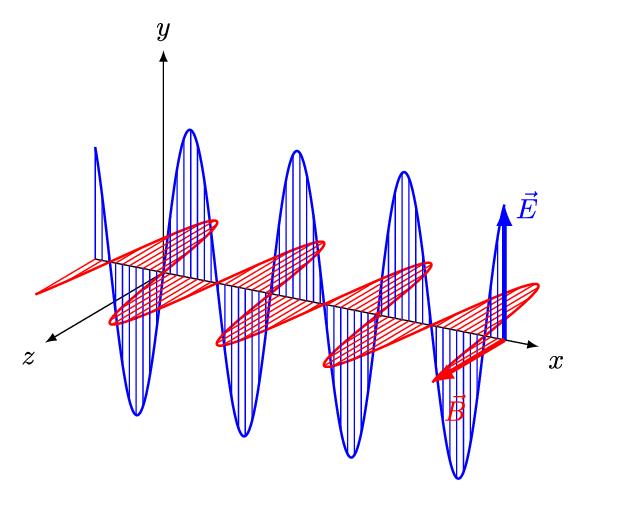
When an electron is in motion, i.e., if there is some current running through some electrical component (like a wire), then an oscillating electric field is produced [2-7]. This oscillating electric field, in turn, generates an oscillating magnetic field. The planes of oscillation of the electric and magnetic fields are orthogonal to each other (see figure 1). This results in an electromagnetic wave which travels at the speed of light c.
Any wave traveling at speed can be mathematically described as
Therefore, for an electromagnetic wave, where the speed is the speed of light we get,
Here, is known as the d’Alembertian operator, which can be thought of as a four-dimensional Laplacian operator [8-12], with an additional time-derivative component.
2.1 Faraday’s Law of Electromagnetic Induction
There are really two aspects to Faraday’s law of electromagnetic induction. These are formulated in terms of two laws, as follows:
2.1.1 First Law
Whenever a conductor is placed in a time-varying magnetic field, an electromotive force (emf) is induced in it [2-7]. Then, if we connect the conductor to a circuit and close it, a current is induced in the circuit, called the induced current. The induced emf around a closed loop is given as the line integral of the electric field along the loop.
| (1) |
Here, is the emf measured in volts (V), and is the electric field generated.
2.1.2 Second Law
The electromotive force around a closed path is equal to the negative of the time rate of change of magnetic flux through the surface which the path encloses. For a loop of wire in a time-varying magnetic field, the magnetic flux is defined by a surface , whose boundary is given by a loop . Since, the loop may be moving, we can write for the surface. Then the magnetic flux is the surface integral given [2-7] as
| (2) |
Here, is the time-varying magnetic field and is the dot product showing the element of magnetic flux through a small element . The magnetic flux through the loop will be proportional to the number of magnetic field components passing perpendicular to the area enclosed by the loop. Subsequently, the magnitude of the emf induced in the circuit will be given according to Faraday’s law [2-7] of electromagnetic induction as
| (3) |
If there are number of turns, or loops in the wire, then we can just multiply the RHS of equation (3) by and the equation will hold true.
2.2 Lenz’s Law
The magnitude of the induced emf is given by the Faraday’s laws of electromagnetic induction. However, emf is not a scalar quantity. It is a vector quantity, and therefore, there is a direction associated with it, which is given by Lenz’s law. Lenz’s law states that the current induced in a circuit due to induced emf (due to changing magnetic field) is directed so as to oppose the change in magnetic flux, and to exert a force which opposes the motion. Mathematically, this adds “direction” to equations (3) and (4).
| (4) |
or in the case of loops,
| (5) |
These equations basically imply that the back emf opposes the changing current, which is the cause of the emf in the first place.
2.3 Transformers and Inductance
One of the most interesting features of Faraday’s laws is that a time-varying current in one coil can induce an emf in a second coil placed close to it. Suppose that we take two coils, each wound around separate bundles of iron sheets (these help to make stronger magnetic fields), as shown in figure 2 below.
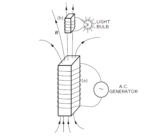
Now, when we connect one of the coils—coil (a)—to
an alternating-current generator. The continually changing current
produces a continuously varying magnetic field. This varying field
generates an alternating emf in the second coil—coil (b). This
emf can, for example, produce enough power to light an electric bulb.
The current in coil (b) can be larger or smaller than the current
in coil (a). The current in coil (b) depends on the emf induced in
it and on the resistance and inductance of the rest of its circuit.
The emf can be less than that of the generator if, say, there is little
flux change. Or the emf in coil (b) can be made much larger than that
in the generator by winding coil (b) with many turns, since in a given
magnetic field the flux through the coil is then greater. Such a combination
of two coils—usually with an arrangement of iron sheets to guide
the magnetic fields—is called a transformer. It can “transform”
one emf (or voltage) to another. This effect is due to the mutual
inductance between the two coils. There are also induction effects
in a single coil. In figure 2, the varying current in coil (a) produces
a varying magnetic field inside itself and the flux of this field
is continually changing, so there is a self-induced emf in coil (a).
This effect is called self-inductance.
The self-inductance of a loop of wire carrying a time-varying current , is given [2-7] as
| (6) |
Here, is the electromotive force induced in the loop. Now, for our purpose, we are more interested in the aspect of mutual inductance, because that is one of the main principles of a transformer. Figure 6 shows an arrangement of two coils, which demonstrates the basic effects responsible for the operation of a transformer.
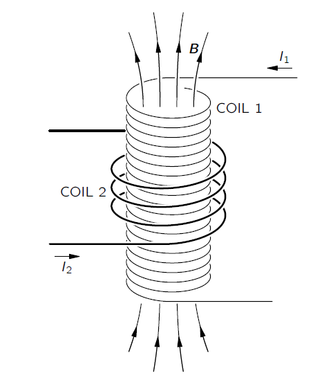
Coil 1 consists of a conducting wire wound in the form of a long solenoid. Around this coil—and insulated from it—is wound coil 2, consisting of a few turns of wire. If now a current is passed through coil 1, we know that a magnetic field will appear inside it. This magnetic field also passes through coil 2. As the current in coil 1 is varied, the magnetic flux will also vary, and there will be an induced emf in coil 2. Suppose the current through coil 1 is , then the emf through coil 1 is given [2-7] as
| (7) |
Here, is the emf induced in coil 1, is the current through coil 2, and is the mutual inductance of the two coils.
2.4 Output Voltage of a Transformer
Suppose we apply a certain amount of output voltage to the primary coil of the transformer (figure 7 shows a basic step-down transformer setup). This means an emf will be generated in the secondary coil with due to mutual induction.
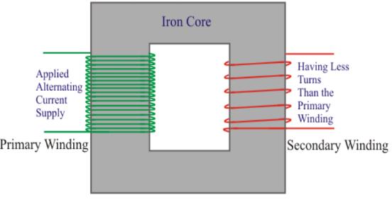
Now, for a step-down transformer, the number of turns of secondary coil is less than the number of turns in the primary coil (). The voltages across the primary and secondary coils ( and respectively) are related to the number of turns ( and respectively) and the currents through them ( and respectively) as,
| (8) |
We will later verify equation (8), by analyzing the data obtained from the computational simulation of the circuit.
2.5 Resonant Transformers
There are various kinds of transformers that one can find. One of
the most efficient transformers is the resonant transformer. A resonant
transformer works on the principle of a resonance in the circuit.
In simple terms resonance is basically the rapid pulsating
(switching on and off) of the current (or voltage) in the circuit.
But how does resonance of the circuit make the transformer more efficient?
Well, the resonance helps to maximise the voltage output of the transformer.
How? We will see that in a while. First, let’s see
how resonance functions in AC and DC circuits.
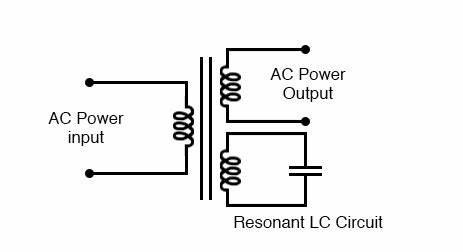
Resonance is generally associated with an AC circuit (i.e., a circuit having an alternating voltage source). But the major problem with using an AC source is that the resonance frequency of the source (the frequency at which the AC source switches the circuit on and off) is not the same as the resulting resonance frequency of the transformer (the frequency at which the transformer coils pulsate). In order to gain the maximum output voltage, these two resonant frequencies need to be made equal in a process known as tuning of a transformer. This tuning of a circuit needs to be done manually by adding some form of external resonance generator to the circuit or by adding some extra load to the transformer via a capacitor (see figure 8 below).
We will discuss why the tuning of the transformer is important later in this section. However, in the case of a DC circuit (like the slayer exciter circuit), the resonance can be generated using a transistor (which acts as a switch to rapidly turn on and off the circuit). In this case, the transformer ends are connected to the transistor and the resonant frequency of the transformer coils is equal to the resonant frequency of the transformer coils. In other words, the transformer is already auto-tuned! Hence, there is no need for the extra hassle to manually tune the circuit. This is indeed what makes a slayer exciter circuit unique in its working and distinguishes it from other types of Tesla coils. But why do we need to tune the transformer in the first place? Let’s look at a famous analogy to understand this. Suppose we have a simple pendulum (a bob suspended by a string; see figure 9 below).
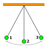
Our problem here is that we want to create the maximum possible
output, i.e., we want the pendulum bob to reach the maximum height
possible. Now imagine the pendulum was already oscillating at a certain
frequency (but the bob was not reaching the maximum possible height).
In order to maximise the height of the bob, we need to apply a force
to it. If we think about it deep enough, we will realize that we can’t
apply the force at any random time. To generate the maximum height,
the force needs to be applied when the bob reaches the extreme points
in its trajectory (points 1 or 3 in figure 9). That’s
the only way the bob can efficiently reach the maximum height. If
we apply a force when it is at the equilibrium point (coming towards
us or going away from us; point 2 in figure 9), the force applied
and the oscillating frequency of the spring won’t be
in sync, and the result will not be maximised. In this analogy, the
oscillating frequency of the pendulum is analogous to the resonant
frequency of the AC source (in case of an AC circuit) or the resonant
frequency of the transistor (in case of a DC circuit); and the force
we apply to the pendulum is analogous to the resonant frequency of
the transformer coils.
One can at least gain an intuition as to why the resonant frequencies need to be equal (i.e., the transformer needs to be tuned) in order to generate the maximum possible output voltage, from the analogy discussed above. This discussion entails all the necessary theory required to move on and perform an experimental analysis of it.
3 Making a Physical Model of the SEC444SEC will be used as a substitute for the Slayer-Exciter Circuit.
While the functioning of a slayer exciter is quite simple to understand, to actually make a physical model requires a significant amount of cautiousness and patience. The following is the process we followed to create the entire slayer exciter physical model666This method is probably the most preliminary one (or a low-cost one), and can be vastly improved upon, using better instrumentation.:
-
•
Gather basic circuit components like n-channel MOSFETs, LEDs, zener diodes, resistors, copper wires, and 9V batteries.
-
•
Use a plywood board to establish the base of the set-up.
-
•
Take a PVC pipe and wind a single strand copper wire around it (approx. 400 windings). This makes the secondary coil of our transformer. This requires a lot of patience, because the winding needs to be perfect in order to make the circuit function as expected.
-
•
Take a thicker copper wire and wind it around the secondary coil (approx. 3-5 windings). Do this as shown in figure 3.
-
•
Connect all the components together to form the circuit shown in figure 7 below (we will explain how these connections are made and how the circuit works later in the report). Use a breadboard if necessary.
-
•
Switch on the battery source.
-
•
Bring a small piece of conducting material close to the transformer. Corona discharges may be observed. Corona discharges are the violet sparks one can see due to the polarization of air surrounding the high voltage transformer. The violet colour is due to the ionization of nitrogen molecules in the air. So, if we bring a conducting material close to the coil, we see a violet spark (corona discharge) between the coil and the conducting material. This step demonstrates the working of our physical slayer exciter circuit.
4 Simulating the SEC
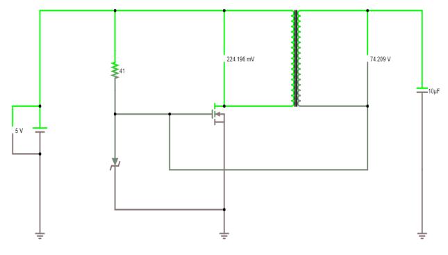
Making the physical model had its own limitations. There was no way we could verify the equation of a transformer (equation 8) using the low-cost physical model, because the measurements would have had a lot of uncertainty, and the results might have been inaccurate. Therefore, we decided to verify the equations graphically using data from an online simulation called Falstad Circuit Applet [1]. This applet is a simulation software based on JavaScript and is very beneficial to analyze any kind of circuit.
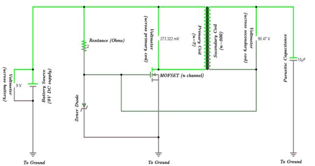
Figure 8 above, shows the final simulated version of the slayer exciter. Let us understand the flow of current in this circuit, with the primary aim of understanding the roles of the different components in the circuit. In figure 9 below, when the battery (B) is turned on, the resistor R drives the current to the base of the transformer (A). Consequently, A turns on and drives the current into the primary coil (PC) of the transformer.
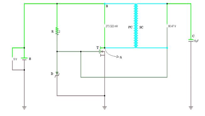
The current is limited by the base current value. This creates
a magnetic field, which induces an emf, and therefore a current in
the secondary coil (SC) of the transformer. The secondary voltage
will tend to grow larger. But the tiny parasitic capacitance on the
output resists this change (although very small) against the rise
of the output end; and so, in return, the voltage on the other end
of the transformer goes down, pulling the base of the transistor low.
The role of the diode (D) is very important to the circuit. Since
we are using a DC input source, the diode prevents the base voltage
to fall more than a minimum specific value below the ground. This
in turn, step’s up the output voltage of the secondary
coil (SC). As a result, the transistor (T) turns off and the magnetic
field starts to reduce. The base voltage increases and A turns on
again and the whole cycle keeps repeating (until the input is cut
off).
The first few questions that come in the mind after looking
at the schematics is that why have we used a MOSFET [13] instead
of a BJT (or for that matter, why have we used a n-p-n transistor
rather than a p-n-p transistor?); or why have we not used an LED instead
of a Zener diode? Well, the reason we used a MOSFET over a BJT, is
because MOSFETs are suitable for high voltage circuits like the slayer
exciter, because it has a very low drain-source. We saw how the current
switching (or resonance) of a circuit helps to maximise the output
voltage. The faster the switching process, the higher will be the
output voltage. Now, the current in a transistor is due to the flow
of majority charge carriers (electrons and holes). Electrons generally
travel faster than holes; and since the majority charge carriers for
n-p-n transistors are electrons, as opposed to p-n-p transistors (which
have holes as the majority charge carriers), we have preferred to
use a n-p-n transistor over a p-n-p transistor.
Coming to the diodes, the reason we did not use a simple
LED is because the input voltage is quite high (almost 14V), and an
LED will fuse out or burn out with a voltage supply as low as 4V!
In contrast, a Zener diode has a much higher input resistance and
can resist higher amounts of input voltage, which is the reason why
we used a Zener diode.
Note: We have provided a link to the simulation text file in the references [14]. Instructions regarding how to initiate the simulation are given in the text file itself.
5 Analyzing the SEC Simulation Data
5.1 Why Perform Analysis?
Any kind of scientific report would be incomplete if it doesn’t provide some tangible results. The physical model of the slayer exciter only serves the purpose of demonstrating its working. But that does not help with any kind of numerical analysis of the circuit. What if we want to know how to maximise the voltage output of the circuit? There certainly isn’t any way of doing that by just looking at the physical model or by looking at its applications. Of course, one could get voltmeters and ammeters and all kinds of output meters to get some kind of data. But what if one doesn’t have all these resources? Well, for that very reason, we sought out for some technique using which we could perform numerical analysis without need of any kind of voltmeters or ammeters or stop-clocks. The best way of doing so was by using the computer simulation we designed in the previous section. We collected the data from the simulation, embedded it into MATLAB, and generated graphical outputs for better visualization.
5.2 What Kind of Analysis?
To serve the purpose of verifying theory, we have decided to plot a graph of how the secondary output voltage varies with time. We will also verify whether the ratio of primary and secondary voltages is equal to the turn ratio of the coil. Barring these, our primary goal is to find an equation that will tell us how to maximise the output voltage by adjusting different parameters in the circuit like resistance, input voltage, inductance, turn ratio and the parasitic capacitance. Lets first see how the output voltage will vary with increasing time.
5.3 Evolution of Output Voltage with Time
We saw in previous sections that the transistor and the transformer have resonant frequencies, which results in the rapid pulsating of current in the circuit. This means that the current, and therefore the voltage change directions as time passes. If we start at time , and observe the change in voltage, we must expect that the voltage traces out a sine curve. Table 1 shows the data for secondary output voltage (; in ) w.r.t. time (; in ), and table 2 shows the values of other parameters, for which the readings were taken.
| Time () | Voltage (V) | Time () | Voltage (V) | Time () | Voltage (V) | Time () | Voltage (V) |
|---|---|---|---|---|---|---|---|
| 0 1.004 | 0 | 12.002 | 155.175 | 24.045 | -36.5 | 36.041 | -146.464 |
| 1.004 | 16.395 | 13.006 | 151.631 | 25.253 | -59.69 | 37.013 | -137.803 |
| 2.042 | 38.879 | 14.003 | 145.094 | 26.005 | -74.618 | 38.005 | -126.28 |
| 3.015 | 59.205 | 15.009 | 135.584 | 27.019 | -93.41 | 39.027 | -111.827 |
| 4 | 78.643 | 16.039 | 122.997 | 28.02 | -110.061 | 40.056 | -94.018 |
| 5.012 | 97.023 | 17.016 | 108.662 | 29 | -124.242 | 41.032 | -77.014 |
| 6.089 | 114.401 | 18.058 | 91.077 | 30.014 | -136.401 | 42.017 | -57.465 |
| 7.007 | 127.128 | 19.011 | 73.264 | 31 | -145.549 | 43.008 | -36.656 |
| 8.001 | 138.496 | 20.056 | 52.234 | 32.007 | -151.962 | 44.022 | -14.65 |
| 9.02 | 147.31 | 21.009 | 32.025 | 33.15 | -155.517 | 45.096 | 8.981 |
| 10.01 | 152.948 | 22.004 | 10.395 | 34.011 | -155.48 | - | - |
| 11.005 | 155.602 | 23 | -11.371 | 35.027 | -152.557 | - | - |
| Parameter | Value |
|---|---|
| Resistance | 22 |
| Capacitance | 10 |
| Primary Inductance | 5H |
| Input Voltage | 10V |
| Turns Ratio | 1000 |
One can easily notice, by looking at the data sets, that the time intervals are not uniform. That is owing to one of the drawbacks of the simulation, that the readings need to be taken manually by pausing the simulation every now and then. Figure 10 below shows the plot of secondary voltage w.r.t. time. As we expected, the nature of the plot is that of a sine curve. Time (s) is plotted on the x-axis and the secondary voltage (V) is plotted on the y-axis.
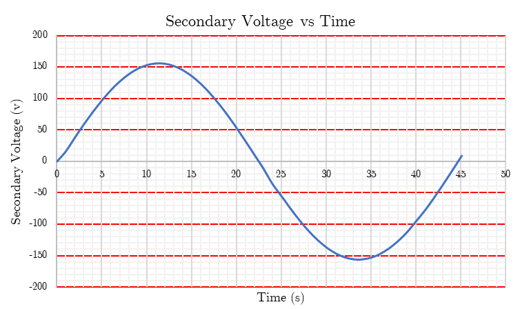
An important thing we can infer from figure 10 is that the transformer takes about 22 seconds to maximise the input voltage from 10V to approximately 156V. The graph also comes out to be symmetrical about the time axis as should be expected from a sine curve of a quantity varying with time. Further, we can say that the curve must represent the equation,
| (9) |
Here, is the secondary output voltage, is the time elapsed, and is the proportionality constant, which will be a combination of the other constant parameters listed in table 2. Note that figure 10 shows only one cycle of resonance in the circuit. This cycle will keep repeating until the input source is switched off.
5.4 Voltage Ratio versus Turn Ratio
According to equation 8, the ratio of secondary to primary voltages of the transformers is proportional to the ratio of the number of turns in secondary to primary coils (i.e. the turn ratio). Table 3 shows the data for voltage ratio and transformer turn ratio, and table 4 shows the values of other constant parameters. The voltage ratio values are not exactly equal to the turn ratio. This is, again, because the readings need to be taken manually by pausing the simulation each time.
| Voltage Ratio | Turns Ratio |
|---|---|
| 100 | 100.708 |
| 200 | 200.197 |
| 300 | 300.296 |
| 400 | 400.398 |
| 500 | 500.499 |
| 600 | 600.593 |
| 700 | 700.693 |
| 800 | 800.799 |
| 900 | 901.239 |
| 1000 | 1000.998 |
| Parameter | Value |
|---|---|
| Resistance | 22 |
| Capacitance | 10 |
| Primary Inductance | 4H |
| Input Voltage | 5V |
Figure 11 below shows the plot of turn ratio versus voltage ratio for the transformer. The curve is a straight line of the nature .
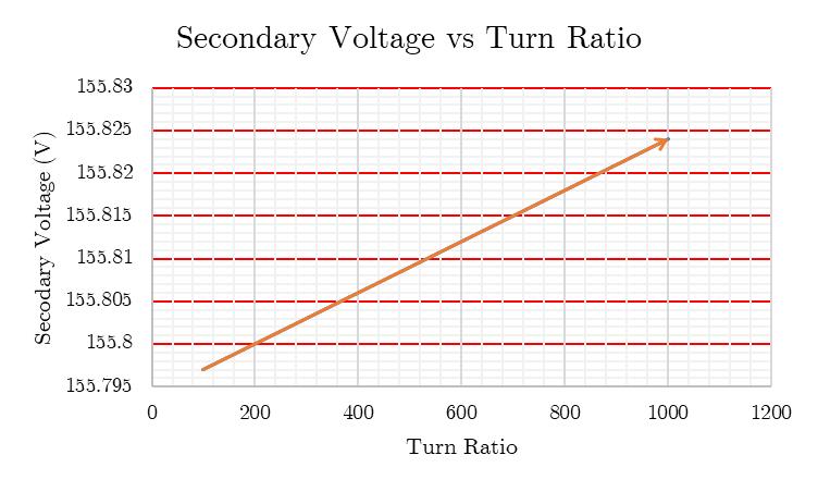
The relation between voltage ratio and turn ratio that we get from figure 11 is shown below in equation 10.
| (10) |
The minor error may be due to the reasons stated before. The analysis uptil this point, helps to verify already existing theory. Now, we will shift our focus towards the main goal of finding an equation to maximise output voltage of the slayer-exciter transformer.
6 Finding an Equation to Maximise SEC Output Voltage
As aforementioned, the main purpose of the simulation is to arrive at an equation, which can tell us (approximately, if not exactly) how we could possibly maximize the output voltage for a given input voltage. Apart from time (; in ) and input voltage (; in V), there are a bunch of other parameters which may or may not affect the output voltage. These are the inductance of the primary coil (; in H), parasitic capacitance (; in ), circuit resistance (; in ), and the turn ratio . Let’s see how the output voltage varies with each of the above-mentioned parameters, and then we can possibly arrive at an equation that relates the output voltage (; in V) to , , and .
6.1 Variation of with
From equation (7), we can say that the ratio of secondary and primary voltages is same as the ratio of primary and secondary inductance. Voltage is measured in volts (V) and inductance is measured in Henries (H).
| (11) |
Combining equation (11) with equation (8),
| (12) |
Now let us understand why increasing the primary inductance leads to an increase in the secondary voltage even if the two quantities are not related in any way. Suppose we increase in equation (12). This won’t have any effect on , , or . But since is increased, the voltage across the primary will also increase. Since , and remain constant, the only way equation (12) is satisfied, is if the secondary voltage (). Hence, even though the primary inductance () and secondary output () are not related in any way, to keep the ratio relation constant, increases when is increased and vice-versa. Table 5 shows the data collected for output voltage and primary inductance and table 6 shows the values for other parameters.
| Secondary Voltage (V) | Primary Inductance (H) |
|---|---|
| 69.746 | 1 |
| 155.788 | 5 |
| 220.268 | 10 |
| 269.741 | 15 |
| 311.453 | 20 |
| Parameter | Value |
|---|---|
| Resistance | 22 |
| Input Voltage | 10V |
| Capacitance | 10 |
| Turns Ratio | 1000 |
Figure 12 below shows the plot of vs . The primary inductance is plotted on the -axis and the output voltage on -axis. The result is as expected. The secondary voltage increases with the primary inductance.
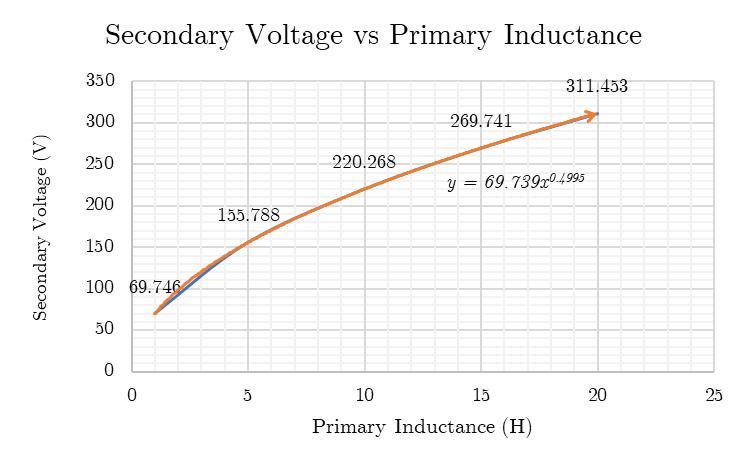
The mathematical relation between and comes out as,
| (13) |
Here, is the output voltage at secondary and is the inductance of the primary coil.
6.2 Variation of with
As discussed before, a parasitic capacitance (in ) exists naturally between the secondary coil of the transformer and the ground. As we know, a capacitor stores electrical energy; and for doing so, if it needs to keep the charge across it’s plates constant, it needs to resist any increase in voltage. In other words, capacitance is a ratio of charge and voltage. Therefore, for a given charge, voltage decreases with increasing capacitance.
| (14) |
Since the parasitic capacitance is connected to the secondary transformer, it resists any change in the secondary output voltage () beyond a certain maximum value. Owing to this reasoning, we must expect that decreases with increasing . More the capacitance, more will be the resistance against changing voltage, and hence, lesser will be the secondary voltage. Table 7 shows the data for capacitance (in ) and secondary voltage (in V); and table 8 shows the values of other constant parameters.
| Capacitance () | Secondary Voltage (V) |
|---|---|
| 1 | 279.833 |
| 2 | 213.235 |
| 3 | 179.421 |
| 4 | 157.064 |
| 5 | 140.666 |
| 6 | 129.177 |
| 7 | 119.754 |
| 8 | 111.801 |
| 9 | 105.676 |
| 10 | 100.264 |
| Parameter | Value |
|---|---|
| Input Voltage | 5V |
| Resistance | 22 |
| Primary Inductance | 5H |
| Turns Ratio | 1000 |
Figure 13 below shows the plot of variation of with . The blue curve is the original plot and the orange curve is the most accurate trend-line. Clearly, as expected, the secondary voltage decreases with increasing capacitance.
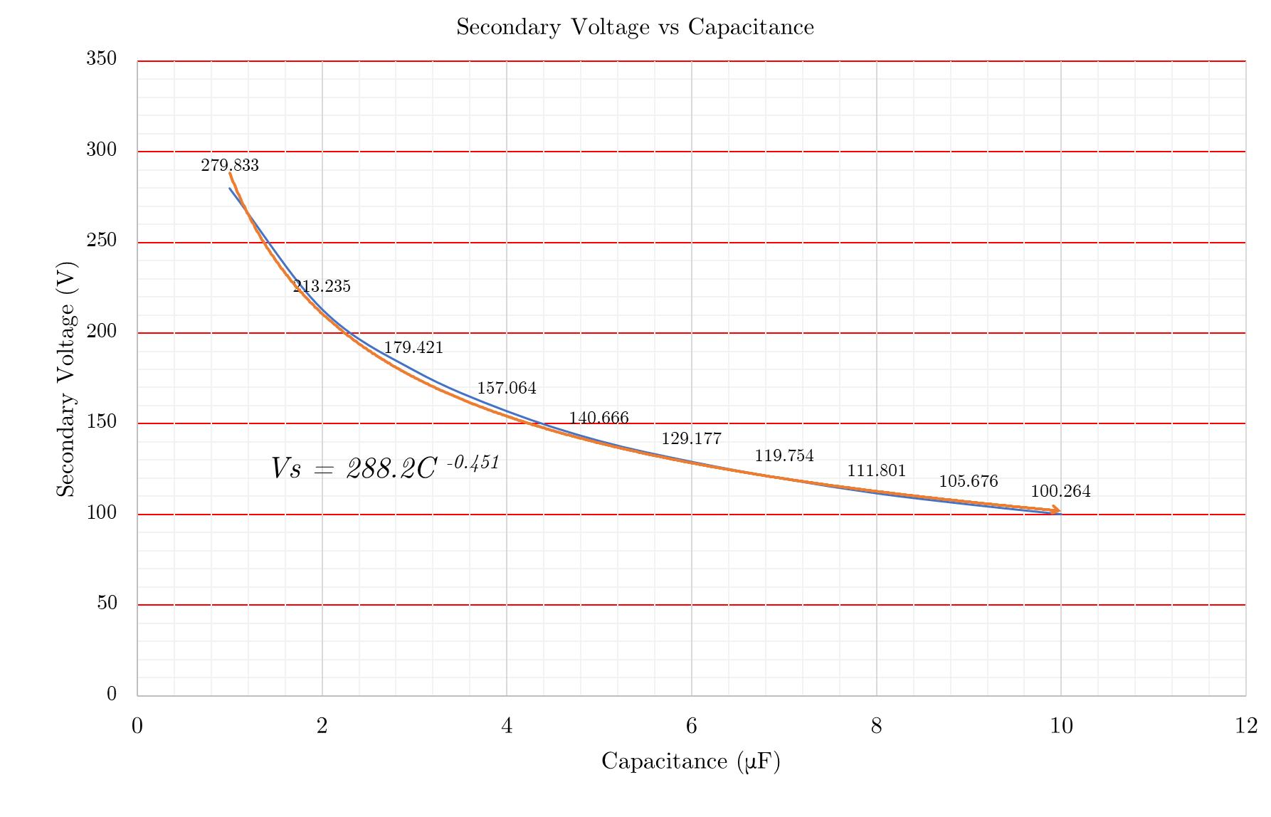
The relation between and is given from figure 13, by the equation,
| (15) |
In equation (15), is the secondary voltage and is the value of the parasitic capacitance. The capacitance may again vary with the separation between the secondary coil of the transformer and the ground.
6.3 Variation of with
We know that the voltage is inversely proportional to resistance. Hence, we expect that the secondary voltage () will also be related similarly to the circuit resistance (). Table 9 shows the data for circuit resistance (in ) and secondary voltage (in V); and table 10 shows the values of other constant parameters.
| Secondary Voltage (V) | Resistance () |
|---|---|
| 157.145 | 10 |
| 155.959 | 20 |
| 155.257 | 30 |
| 154.779 | 40 |
| 154.395 | 50 |
| 154.076 | 60 |
| 153.822 | 70 |
| 153.576 | 80 |
| 153.352 | 90 |
| 152.921 | 100 |
| Parameter | Value |
|---|---|
| Input Voltage | 10V |
| Capcitance | 10 |
| Primary Inductance | 5H |
| Turns Ratio | 1000 |
Figure 14 below shows the plot for versus . The variation with resistance is not exactly of the “inverse” nature, which might be because the resistance of the entire circuit is not taken into consideration. Only the primary resistance provided by the resistor has been considered.
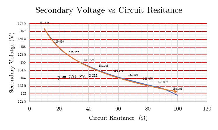
The relation between and is described by the sec,
| (16) |
Here, is the secondary voltage and is the circuit resistance.
6.4 Variation of with
According to equation (8), for a given primary voltage (), the secondary voltage () will increase with the turn ratio of the transformer , where and are the number of turns of the secondary and primary coils respectively. Table 11 shows the data for turn ratio of the transformer and the corresponding voltage produced at the secondary coil; and table 12 shows the values for other constant parameters.
| Secondary Voltage (V) | Turns Ratio |
|---|---|
| 155.797 | 100 |
| 155.8 | 200 |
| 155.803 | 300 |
| 155.806 | 400 |
| 155.809 | 500 |
| 155.812 | 600 |
| 155.815 | 700 |
| 155.818 | 800 |
| 155.821 | 900 |
| 155.824 | 1000 |
| Parameter | Value |
|---|---|
| Resistance | 22 |
| Capacitance | 10 |
| Primary Inductance | 5H |
| Input Voltage | 5V |
Figure 15 below shows the plot of secondary voltage versus turn ratio of the transformer. As expected, the relation is linear in nature, i.e., the secondary voltage increases with the turn ratio.

The relation between the secondary voltage and turn ratio is given from figure 15, by the equation,
| (17) |
Here, is the secondary voltage and is the turn ratio of the transformer.
6.5 Equation of the SEC
In sections 6.1. through section 6.4., we have arrived at approximate relations between the secondary voltage () and other parameters like primary inductance (), parasitic capacitance (), circuit resistance () and transformer ratio . We are now in a position to derive an equation from our experimental findings. From equations (13), (15), (16) and (17), we see that,
Combining these, we get,
| (18) |
In equation (18), is the secondary voltage, is the primary inductance, is the circuit resistance and is the transformer turn ratio. The proportionality constant () depends on the accuracy of measurement. In other words, the more accurately we measure the different parameters, the more accurate equation (18) gets. Equation (17) is the equation we required. We call this equation the “SEC Equation”. One can call it anything really, because it’s just a name! This equation tells us how we can maximise the output voltage at the secondary coil of transformer, for a given source voltage, by varying different parameters of the SEC.
7 The Apparent Error in the SEC Equation
Before we get too excited by equation (18), it would be better to see how approximate the equation is to the actual expected equation. First of all, what is the actual expected equation? Well as we just discussed in previous sections (equations (6), (12) and (14)), the secondary voltage should vary with other parameters as follows:
Combining these we get,
| (19) |
Certainly, we can see that equation (18), which we got using the simulation is not a good approximation of the actual equation (19). The most immediate question that comes to mind is why does this difference exist between equation (18) and equation (19)? Well that might be because that measurement using the simulation is a highly error-prone process. Measurement (as stated before) needs to be done manually by pausing the simulation every now and then, and noting down the various parameter values. As mentioned previously, the more accurate the measurement, the more equatio (18) will start to look like equation (19).
8 Potential Sources of Error
There are a number of logical precautions and potential sources of error, that may occur while preparing the physical model, as well as the simulated model.
8.1 Physical Model
-
•
The connections may be improper or loose.
-
•
Components may be defective.
-
•
Circuit might get overheated if kept running for a long time. Due to this, components may get damaged.
8.2 Simulated Model
-
•
The simulation has no means to automatically export data. Hence, data has to be obtained manually by pausing the simulation frequently. This may result in some minor errors while measurement of parameters.
-
•
Components in the simulation may be improperly connected. For instance, the Zener diode may be connected in forward bias.
9 Results and Concluding Remarks
-
•
According to the data analysis from simulation, for a given source voltage, the secondary voltage changes with parasitic capacitance, circuit resistance, primary inductance and turn ratio as follows:
-
•
According to theory, for a given source voltage, the secondary voltage changes with parasitic capacitance, circuit resistance, primary inductance and turn ratio as follows:
-
•
The output voltage secondary varies as a sine function of the time elapsed.
-
•
The proportionality constant k in the above equations depends on the accuracy of measurement of various parameters.
References
- [1] Falstad Circuit Simulation Applet: http://www.falstad.com/circuit/circuitjs.html
- [2] Feynman, R. P., R .B. Leighton, and M. Sands, 1965, The Feynman Lectures on Physics, Vol. II: the Electromagnetic Field, Addison-Wesley, Reading, Massachusetts.
- [3] Griffiths, David J. (2013). Introduction to Electrodynamics (4th ed.). Boston, Mas.: Pearson.
- [4] Panofsky, W. K., and M. Phillips, 1969, Classical Electricity and Magnetism, 2nd edition, Addison-Wesley, Reading, Massachusetts
- [5] Jackson, John D. (1998). Classical Electrodynamics (3rd ed.). New York: Wiley.
- [6] David M Cook (2002). The Theory of the Electromagnetic Field. Mineola NY: Courier Dover Publications. p. 335 ff.
- [7] James Clerk Maxwell, "A Dynamical Theory of the Electromagnetic Field", Philosophical Transactions of the Royal Society of London 155, 459–512 (1865).
- [8] Courant, Richard; Hilbert, David (1989), Methods of Mathematical Physics, New York: Interscience Publishers.
- [9] Arfken, George B.; Weber, Hans J. (1995), Mathematical methods for physicists (4th ed.), San Diego: Academic Press.
- [10] Boas, Mary L. (2006), Mathematical Methods in the Physical Sciences (3rd ed.), Hoboken: John Wiley & Sons.
- [11] Hassani, Sadri (1999), Mathematical Physics: A Modern Introduction to Its Foundations, Berlin, Germany: Springer-Verlag.
- [12] Butkov, Eugene (1968), Mathematical physics, Reading: Addison-Wesley.
- [13] Wann, Clement & Noda, Kenji & Tanaka, Tetsu & Yoshida, Makoto & hu, Chenming. (1996). A comparative study of advanced MOSFET concepts. Electron Devices, IEEE Transactions on. 43. 1742 - 1753. 10.1109/16.536820.
- [14] Code: https://drive.google.com/file/d/1xnTnIfxUGWvO4511rK81KHAQGVhJ5WLr/view?usp=sharing