Magnetoconductance modulations due to interlayer tunneling in radial superlattices
Abstract
Radial superlattices are nanostructured materials obtained by rolling-up thin solid films into spiral-like tubular structures. The formation of these “high-order” superlattices from two-dimensional crystals or ultrathin films is expected to result in a transition of transport characteristics from two-dimensional to one-dimensional. Here, we show that a transport hallmark of radial superlattices is the appearance of magnetoconductance modulations in the presence of externally applied axial magnetic fields. This phenomenon critically relies on electronic interlayer tunneling processes that activates an unconventional Aharonov-Bohm-like effect. Using a combination of density functional theory calculations and low-energy continuum models, we determine the electronic states of a paradigmatic single-material radial superlattice – a two-winding carbon nanoscroll – and indeed show momentum-dependent oscillations of the magnetic states in axial configuration, which we demonstrate to be entirely due to hopping between the two windings of the spiral-shaped scroll.
Department of Physics, National Cheng Kung University, Tainan 701, Taiwan
Center for Quantum Frontiers of Research & Technology (QFort), National Cheng Kung University, Tainan 701, Taiwan
Department of Physics, National Tsing Hua University, Hsinchu 30013, Taiwan
Center for Quantum Technology, National Tsing Hua University, Hsinchu 30013, Taiwan
IFW Dresden and Würzburg-Dresden Cluster of Excellence ct.qmat, Helmholtzstrasse 20, 01069 Dresden, Germany
Institute of Physics, Academia Sinica, Taipei 11529, Taiwan
Department of Physics, National Taiwan Normal University, Taipei 11677, Taiwan
Institute for Theoretical Physics, Center for Extreme Matter and Emergent Phenomena, Utrecht University, Princetonplein 5, NL-3584 CC Utrecht, Netherlands
Dipartimento di Fisica “E. R. Caianiello”, Universitá di Salerno, IT-84084 Fisciano, Italy
∗To whom correspondence should be addressed; E-mail: cutygo@phys.ncku.edu.tw.
Since the pioneering work of Esaki and Tsu back in the 1970 [1], superlattices have introduced a new paradigm for the synthesis of artificial nanoscale material structures with tailored electronic properties. The synthesis of moiré superlattices of two-dimensional van der Waals materials, obtained for instance by placing single-layer graphene on aligned hexagonal boron-nitride substrates [2, 3, 4, 5, 6], has led to the experimental observation of superlattice minibands forming the well-known Hofstadter butterfly[7] and the related generation of Dirac cone replicas [8, 9, 10, 11, 12, 13]. Likewise, the moiré superlattice of magic-angle twisted bilayer graphene has been to shown to yield flat bands associated with emerging correlated insulating behavior and superconductivity [14, 15]. Rolled-up nanotechnology [16, 17, 18, 19] – a strain-induced technique able to tune planar ultrathin films into complex three-dimensional nanoarchitectures – provides yet another route to superlattices. The rolling-up mechanism can be applied to a huge variety of materials, including metals, insulators, polymers and traditional semiconductor families. Functional properties such as the thermal conductivity have been shown to be geometrically tailored in silicon radial superlattices [20]. Very recently, the rolled-up nanotechnology has been also applied to two-dimensional van-der-Waals materials to create high-order van der Waals superlattices [21]. Independent of the material at hand, the preparation of these material structures is expected to modulate, via the effective change of dimensionality, their electronic properties, thereby leading to unconventional transport behavior. For instance, a distinctive property of tubular structures with spiral-like cross sections is that they break the rotational symmetry in the embedding three-dimensional space. As a result, their longitudinal magnetoresistance can exhibit a marked directional dependence [22]. This angle-dependent magnetoresistance has been predicted to occur in the ballistic regime when considering rolled-up nanotubes made out of conventional semiconducting materials. The same effect is expected to appear[23] , however, also in the diffusive regime characterizing transport in, e.g., carbon nanoscrolls: spirally wrapped graphite layers [24]. The report of an angle-dependent magnetoresistance behavior in SnS2/WSe2 rolled-ups has provided experimental evidence for the occurrence of this geometry-induced effect [21] . The aim of this work is to show that another transport hallmark of radial superlattices is the appearance of magnetoconductance modulations in the presence of externally applied axial magnetic fields.
When subject to axial magnetic fields tubular structures with cross-sections forming closed loops display the well-known Aharonov-Bohm (AB) effect [25], which leaves distinctive fingerprints. Aharonov-Bohm (AB) magnetoresistance oscillations have been reported in multiwalled carbon nanotubes (CNT) [26]. Furthermore, the AB effect has been predicted to induce a semimetal to semiconductor transition in single-walled CNTs [27, 28]. Distinctive signatures of the structural symmetry of semiconducting core-shell nanowires can be also inferred from the AB oscillations of the energy levels [29]. Finally, characteristic fingerprints of the anomalous metallic states in three-dimensional topological insulator nanowires [30] can be also identified from their associated AB effect.
The open cross section of a radial superlattice prevents a full phase interference between electronic waves traveling in opposite direction at the origin of the AB effect. Any magnetoconductance oscillations in an axial configuration should be therefore completely prevented. Contrary to such expectations, we will instead show that radial superlattices can and do display magnetoconductance oscillations when an axial magnetic field is externally applied. Using a combination of density functional theory and an effective continuum low-energy model, we will theoretically prove that a carbon nanoscroll (CNS) – a prototypical radial superlattice – displays oscillations of the energy levels when subject to an axial magnetic field even in a minimal two-winding geometry. This effect is entirely due to the tunneling between the two consecutive windings of the spiral structure as proved by the fact that the energy level oscillations disappear by artificially switching off the interlayer coupling. We furthermore prove that the amplitude of the energy level oscillations is strongly dependent upon the momentum in the translationally invariant axial direction of the scroll.
We start out by illustrating the mechanism responsible for the onset of magnetoconductance oscillations in a spiralling two-winding carbon nanoscroll. Its geometry is explicitly shown in Fig. 1(a). Note that the axial, translationally invariant direction, corresponds to a zigzag direction of the honeycomb lattice. As sketched in Figs. 1(b),(c) the interlayer structure is equivalent to the Bernal AB stacking in bilayer graphene. Therefore, the largest hopping amplitude in the structure corresponds to the interlayer hopping between “dimer” sites [see Fig. 1(c)]. Consider now the unrolled nanostructure along the azimuthal direction as shown in Fig. 1(d). The strong dimerization between the two layers implies that at each azimuthal angle the electronic wavefunction has a sizable probability amplitude on both the lower and the upper graphene layers. At the open edges explicitly marked in Fig. 1(d), on the other hand, the lower and upper graphene layers have to continuously evolve one into the other in order to reconstruct a two-winding scroll. Consequently, the dimerized electronic wavefunction is “partially” embedded in a closed geometry. Therefore, and as a result of the interlayer tunneling, the system can react to an electromagnetic potential precisely as in the conventional AB effect.
To concretely prove the appearance of such unconventional AB effect, we model a two-winding CNS with the low-energy of bilayer graphene along the arclength ( axis) of the nanostrucure while concomitantly using special boundary conditions that allow for the tunneling between the two layers (see Fig. 1(e) and (f)).
Specifically we use the effective four band model for the 2pz orbitals on the four atomic sites of the unit cell. It can be written as follows: [31]
| (1) |
where the momentum operators are and with along the CNS axis and along the arclength direction. In addition, is the valley index that distinguishes between the two inequivalent K points in the Brillouin zone. The Fermi velocity reads as , where is the intralayer hopping amplitude between sites A1 and B1 (or A2 and B2). Finally, we explicitly consider the interlayer coupling between the dimer sites A2 and B1 , as shown in Fig. 1.

The energy for Eq. (1) is given by , where distinguishes between the valence and conduction band. Furthermore, the left-moving and right-moving wave functions read as
| (2) |
where is a normalization constant.
Within our continuum model, the electronic band structure of the two-winding CNS can be obtained by superimposing the boundary conditions sketched in Fig. 1(f). They are given by:
| (3) |
where is the radius of the CNSs, with the total arclength of each layer given by .
To fit the boundary conditions Eq. (3), we write a generic wave function , which is a combination of the left-moving and right-moving wave functions in the conduction and valence bands . In other words, we write the generic wave function as where , , , and are coefficients that we fix by imposing the boundary conditions.
We also use the following microscopic tight-binding parameters: The lattice constant is Å[32], whereas the intralayer and interlayer couplings are eV and eV, respectively [33, 31]. We also take the arclength of each layer nm. Thus the total arclength of the two-winding nanoscroll is nm.
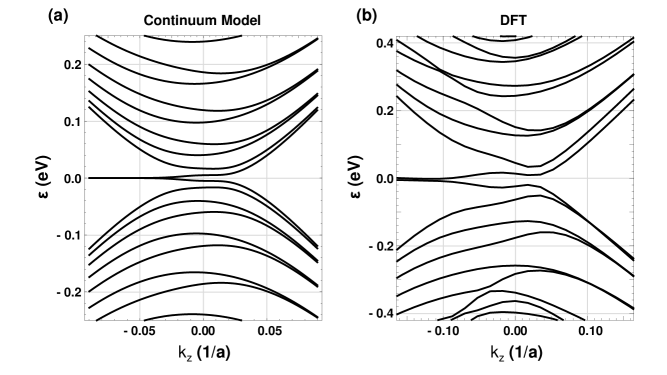
Fig. 2(a) shows the energy bands of the two-winding CNSs obtained from our continuum model. The is the projection of the high-symmetry K point, i.e. the Dirac point in monolayer graphene. In perfect analogy with the states found in graphene nanoribbons with zigzag edges, we find that also our two-winding carbon nanoscroll display edge states for momenta [see Fig. 2(a)]. The density profiles of edge and bulk-like states and their -dependent evolutions are provided in Supplementary Information (Section S1). In order to establish that the continuum model provides an accurate description of the electronic structure of a two-winding CNS, we have thereafter performed density functional theory (DFT) calculations using the structure shown in Fig. 1(a) to (d). We provide details of the DFT calculations in Supplementary Information (Section S2). As demonstrated in Fig. 2, there is an excellent agreement between the electronic structure obtained using DFT and our effective model. This consequently allows us to study the effect of an externally applied axial magnetic field using the low-energy model.
.
To investigate the effect of an externally applied homogeneous axial magnetic field we, as usual, use a minimal coupling with the vector potential, , related to the externally applied axial magnetic field by . Since the applied axial magnetic field is considered, , we introduce the canonical momenta given by . The vector potential can be expressed as usual as , where is the magnetic flux and is the angle around the cylinder [35], and more clearly it is given as [22]. Thus, we have that the wave factors in the wave functions with applied magnetic field must be written as and . Here we introduced the flux quantum is given by with being electronic charge.
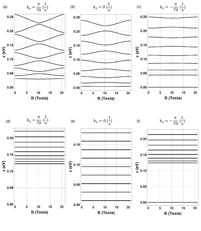
Fig. 3 shows our main finding: the oscillations of the energy levels as a function of the axial magnetic field intensity for different values of the transversal momentum in a structure where the conventional AB effect is precluded. Note that the amplitude of the oscillations is enhanced for and more attenuated by decreasing the longitudinal momentum toward the region.
This result indicates that the electronic states with in the nanoscroll are similar in nature to the states in a flat “unrolled” bilayer graphene nanoribbon which, due to the open geometry, are not expected to display energy oscillations. As proved in the Supplementary Information (Sections S4 and S6) these states without oscillations of the magnetic energy levels satisfy the following criterion on their tube axis momentum
| (4) |
An example of the states satisfying the criterion above is shown in Fig. 3(c). We also emphasize that also the zero energy edge state [see Fig.2] also satisfy this criterion and thus is not practically affected by the electromagnetic potential. We finally note that the criterion in the opposite valley simply interchanges the sign of the transversal momentum as mandated by time-reversal invariance.
In Fig. 3 we also present the magnetic energy states by artificially neglecting the dimer interlayer hopping amplitude . The magnetic oscillations of the energy levels are completely absent thus demonstrating that the presence of our unconventional AB effect in a spiral open structure is entirely due to electronic tunneling between the layers.
We finally evaluate the consequence of the oscillations of the magnetic energy levels in transport. In particular, we consider the two-terminal conductance in the ballistic regime. We therefore use the Landauer formula [36, 37, 22],
| (5) |
where denotes as the Fermi-Dirac distribution function, and is the Fermi energy. As usual, is the conductance at zero temperature, which is simply given by the number of occupied bands in our quasi-one-dimensional nanostructure. Note also that we do not account for the small spin-orbit coupling of graphene and therefore the spin simply gives a multiplicity two to the conductance.
We show the behavior of the conductance in the absence and presence of an axial magnetic field in Fig. 4. The oscillations of the magnetic energy levels is reflected in a finite magnetoconductance as evidenced by the change of ballistic conductance as the field strength is varied. In Fig. 4(a), low temperature and without applied magnetic field case (10 K and 0 Tesla), the widths of plateaux vary alternatively between large and small. It is similar to the magnetic case; yet for magnetic field case (10 K and 10 Tesla), plateaux change their narrow ones to broad, and vise versa. The similar phenomena occur in the high temperature (50 K) (Fig. 4(b)) and the medium temperature (25 K) (Fig. S10 in Supplementary Information). In the low-temperature regime, we have the conventional quantization in units of of a quantum point contact [38] with different plateaus as we sweep the Fermi energy (see Fig. 4(a)). The difference in the plateaux structure in the presence of the axial magnetic field is the fingerprint of the the magnetoconductance modulations. Note that the axial magnetic field effects on the two terminal conductance persist even in the high temperature regime where the quantization of the conductance is lost due to the thermal smearing, as is shown in Fig. 4(b).

To wrap up, we have considered with a combination of DFT calculations and an effective low-energy model, the electronic properties of a two-winding CNSs and established in the presence of an axial magnetic field the occurrence of oscillations of the magnetic energy levels as the intensity of the magnetic field is increased. We have found that because of the presence of an interlayer tunneling there is an unconventional Aharonov-Bohm-like effect with electrons responding to an electromagnetic potential even if the structure does not possess a closed cylindrical geometry. In addition, the presence of both bulk and edge states yields a different oscillation amplitude of the energy levels for different values of the momentum along the nanoscroll axis. We demonstrate this feature of magnetoconductivity is originated from a unique nature of the nanoscroll – its states varies between the tube states and the ribbon states when the momentum changes.
This newly established phenomenon is not specific of carbon nanoscrolls. It can indeed appear in different radial superlattices obtained by rolled-up technology including the recently synthesized high-order van der Waals superlattices. Moreover, its presence is very robust against moderate disorder (see Section S6 in Supplementary Information). Since in all these nanostructures electronic tunneling between the various layers is present, we expect the effect we have unveiled in our work to be observable in the experimental realm.
Acknowledgements
We acknowledge the financial support by the Ministry of Science and Technology (Grants No. MOST-107-2112-M006-025-MY3, No. MOST-108-2638-M-006-002-MY2, No. MOST 110-2112-M-006-020-, and No. MOST 110-2112- M-003-008-MY3) and National Center for Theoretical Sciences in Taiwan. C. O. acknowledges support from a VIDI grant (Project 680-47-543) financed by the Netherlands Organization for Scientific Research (NWO). C.-H. C. acknowledges support from the Yushan Young Scholar Program under the Ministry of Education (MOE) in Taiwan. We acknowledge technical assistance by Botsz Huang and You-Ting Huang. The authors gratefully acknowledge many helpful discussions with Szu-Chao Chen, Hsiu-Chuan Hsu, Ion Cosma Fulga, Chao-Cheng Kaun, Chao-Ping Hsu, and Chong-Der Hu.
References
References
- [1] Esaki, L. & Tsu, R. Superlattice and negative differential conductivity in semiconductors. IBM Journal of Research and Development 14, 61–65 (1970).
- [2] Tang, S. et al. Precisely aligned graphene grown on hexagonal boron nitride by catalyst free chemical vapor deposition. Scientific Reports 3, 2666 (2013).
- [3] Roth, S., Matsui, F., Greber, T. & Osterwalder, J. Chemical vapor deposition and characterization of aligned and incommensurate graphene/hexagonal boron nitride heterostack on cu(111). Nano Letters 13, 2668–2675 (2013).
- [4] Tang, S. et al. Silane-catalysed fast growth of large single-crystalline graphene on hexagonal boron nitride. Nature Communications 6, 6499 (2015).
- [5] Dean, C. R. et al. Boron nitride substrates for high-quality graphene electronics - Nature Nanotechnology. Nat. Nanotechnol. 5, 722–726 (2010).
- [6] Woods, C. R. et al. Commensurate–incommensurate transition in graphene on hexagonal boron nitride - Nature Physics. Nat. Phys. 10, 451–456 (2014).
- [7] Hofstadter, D. R. Energy levels and wave functions of bloch electrons in rational and irrational magnetic fields. Phys. Rev. B 14, 2239–2249 (1976).
- [8] Ponomarenko, L. A. et al. Cloning of dirac fermions in graphene superlattices. Nature 497, 594–597 (2013).
- [9] Dean, C. R. et al. Hofstadter’s butterfly and the fractal quantum hall effect in moirésuperlattices. Nature 497, 598–602 (2013).
- [10] Hunt, B. et al. Massive dirac fermions and hofstadter butterfly in a van der waals heterostructure. Science 340, 1427–1430 (2013).
- [11] Yankowitz, M. et al. Emergence of superlattice Dirac points in graphene on hexagonal boron nitride - Nature Physics. Nat. Phys. 8, 382–386 (2012).
- [12] Ortix, C., Yang, L. & van den Brink, J. Graphene on incommensurate substrates: Trigonal warping and emerging Dirac cone replicas with halved group velocity. Phys. Rev. B 86, 081405 (2012).
- [13] Wallbank, J. R., Patel, A. A., Mucha-Kruczyński, M., Geim, A. K. & Fal’ko, V. I. Generic miniband structure of graphene on a hexagonal substrate. Phys. Rev. B 87, 245408 (2013).
- [14] Cao, Y. et al. Unconventional superconductivity in magic-angle graphene superlattices - Nature. Nature 556, 43–50 (2018).
- [15] Cao, Y. et al. Correlated insulator behaviour at half-filling in magic-angle graphene superlattices - Nature. Nature 556, 80–84 (2018).
- [16] Schmidt, O. G. & Eberl, K. Thin solid films roll up into nanotubes - Nature. Nature 410, 168 (2001).
- [17] Xu, C., Wu, X., Huang, G. & Mei, Y. Rolled-up Nanotechnology: Materials Issue and Geometry Capability. Adv. Mater. Technol. 4, 1800486 (2019).
- [18] Chen, Z., Huang, G., Trase, I., Han, X. & Mei, Y. Mechanical Self-Assembly of a Strain-Engineered Flexible Layer: Wrinkling, Rolling, and Twisting. Phys. Rev. Appl. 5, 017001 (2016).
- [19] Deneke, C., Songmuang, R., Jin-Phillipp, N. Y. & Schmidt, O. G. The structure of hybrid radial superlattices. J. Phys. D: Appl. Phys. 42, 103001 (2009).
- [20] Li, G. et al. In-Plane Thermal Conductivity of Radial and Planar Si/SiOx Hybrid Nanomembrane Superlattices. ACS Nano 11, 8215–8222 (2017).
- [21] Zhao, B. et al. High-order superlattices by rolling up van der Waals heterostructures. Nature 591, 385–390 (2021).
- [22] Chang, C.-H., van den Brink, J. & Ortix, C. Strongly Anisotropic Ballistic Magnetoresistance in Compact Three-Dimensional Semiconducting Nanoarchitectures. Phys. Rev. Lett. 113, 227205 (2014).
- [23] Chang, C.-H. & Ortix, C. Theoretical Prediction of a Giant Anisotropic Magnetoresistance in Carbon Nanoscrolls. Nano Lett. 17, 3076–3080 (2017).
- [24] Xie, X. et al. Controlled Fabrication of High-Quality Carbon Nanoscrolls from Monolayer Graphene. Nano Lett. 9, 2565–2570 (2009).
- [25] Aharonov, Y. & Bohm, D. Significance of Electromagnetic Potentials in the Quantum Theory. Phys. Rev. 115, 485–491 (1959).
- [26] Bachtold, A. et al. Aharonov–Bohm oscillations in carbon nanotubes. Nature 397, 673–675 (1999).
- [27] Tian, W. & Datta, S. Aharonov-Bohm-type effect in graphene tubules: A Landauer approach. Phys. Rev. B 49, 5097–5100(R) (1994).
- [28] Ando, T. Aharonov–bohm effect and symmetry crossover in carbon nanotubes. Journal of the Physical Society of Japan 75, 054701 (2006).
- [29] Ferrari, G., Goldoni, G., Bertoni, A., Cuoghi, G. & Molinari, E. Magnetic States in Prismatic Core Multishell Nanowires. Nano Lett. 9, 1631–1635 (2009).
- [30] Bardarson, J. H., Brouwer, P. W. & Moore, J. E. Aharonov-Bohm Oscillations in Disordered Topological Insulator Nanowires. Phys. Rev. Lett. 105, 156803 (2010).
- [31] McCann, E. & Koshino, M. The electronic properties of bilayer graphene. Reports on Progress in Physics 76, 056503 (2013).
- [32] Saito, R., Dresselhaus, G. & Dresselhaus, M. S. Physical Properties of Carbon Nanotubes (World Scientific Publishing Company, London, England, UK, 1998).
- [33] Kuzmenko, A. B., Crassee, I., van der Marel, D., Blake, P. & Novoselov, K. S. Determination of the gate-tunable band gap and tight-binding parameters in bilayer graphene using infrared spectroscopy. Phys. Rev. B 80, 165406 (2009).
- [34] Owing to the limitation of system size in DFT simulation, we utilize a smaller unit cell of CNS with nm. Although the scales of energy and momentum that are differ from the CNS with arclength nm, the characters of energy bands is still remained. has different scale of energy and momentum to nm. To verify the result, we also show the result of the same CNS with an arclength nm by using the tight-binding simulation, as is presented in Fig. S13 in Supplementary Information. .
- [35] Ezawa, Z. F. Quantum Hall Effects: Recent Theoretical and Experimental Developments Third Edition (World Scientific Publishing Company, 2013).
- [36] Landauer, R. Spatial Variation of Currents and Fields Due to Localized Scatterers in Metallic Conduction. IBM J. Res. Dev. 1, 223–231 (1957).
- [37] Bagwell, P. F. & Orlando, T. P. Landauer’s conductance formula and its generalization to finite voltages. Phys. Rev. B 40, 1456–1464 (1989).
- [38] van Wees, B. J. et al. Quantized conductance of point contacts in a two-dimensional electron gas. Phys. Rev. Lett. 60, 848–850 (1988).
- [39] Kresse, G. & Furthmüller, J. Efficient iterative schemes for ab initio total-energy calculations using a plane-wave basis set. Phys. Rev. B 54, 11169–11186 (1996).
- [40] Kresse, G. & Hafner, J. Ab initio molecular dynamics for open-shell transition metals. Phys. Rev. B 48, 13115–13118 (1993).
- [41] Blöchl, P. E. Projector augmented-wave method. Phys. Rev. B 50, 17953–17979 (1994).
- [42] Kresse, G. & Joubert, D. From ultrasoft pseudopotentials to the projector augmented-wave method. Phys. Rev. B 59, 1758–1775 (1999).
- [43] Ceperley, D. M. & Alder, B. J. Ground State of the Electron Gas by a Stochastic Method. Phys. Rev. Lett. 45, 566–569 (1980).
METHODS
0.1 First-principle calculations.
To study the two-winding carbon nanoscrolls (CNSs), first-principle simulations based on density functional theory (DFT) are developed to confirm our model matching to the realistic materials. In the first-principle calculations, the Vienna Ab initio Simulation Package (VASP)[39, 40] with the projector augmented wave (PAW) method [41, 42] is used. The Ceperley-Alder (CA) type local density approximation (LDA) [43] is included as exchange-correlation function. The energy cut off (k-points grid) with 400 eV () is utilized in simulations.
0.2 Data availability.
The data that support the findings of this study are available from the corresponding author upon reasonable request.