Optical fibre-based (plug-and-play) single photon source using InAsP quantum dot nanowires and gradient-index lens collection
Abstract
We present a compact, fibre-coupled single photon source using gradient-index (GRIN) lenses and an InAsP semiconductor quantum dot embedded within an InP photonic nanowire waveguide. A GRIN lens assembly is used to collect photons close to the tip of the nanowire, coupling the light immediately into a single mode optical fibre. The system provides a stable, high brightness source of fibre-coupled single photons. Using pulsed excitation, we demonstrate on-demand operation with a single photon purity of 98.5% when exciting at saturation in a device with a source-fibre collection efficiency of 35% and an overall single photon collection efficiency of 10%. We also demonstrate “plug and play" operation using room temperature photoluminescence from the InP nanowire for room temperature alignment.
Non-classical photon states (e.g. single, indistinguishable, or entangled) form the basis of photonic quantum technologiesO’Brien, Furusawa, and Vučković (2009). For implementation of these technologies in a future quantum network, the efficient transmission of these states between nodes in the network is critical. The most convenient transmission channel is an optical fibre, and in particular, a single-mode fibre (SMF) where photons exist in a single spatial mode. Solid-state two-level systems (e.g. quantum dots, or defects) can produce the required states efficiently and deterministically, but the devices are typically designed to emit into free-space. High efficiency coupling of the free-space mode to the gaussian mode of a SMF can be achieved with external opticsGazzano et al. (2013); Bulgarini et al. (2014); Lee et al. (2021) and, using nearly perfectly matched modes, coupling efficiencies of 93% have been demonstratedBulgarini et al. (2014). To eliminate stability issues related to the alignment of free-space optics, new techniques for coupling to fibres are required. One can, for example, use the cleaved facet of a fibre to form one mirror of a Bragg reflector-based open microcavity allowing for direct collection of the cavity photons into the fibreMuller et al. (2009); Greuter et al. (2015). Alternatively, evanescent coupling via tapered fibres can be applied to collect light from emittersFujiwara et al. (2011); Liebermeister et al. (2014), cavitiesAtes et al. (2013); Lee et al. (2015) or tapered nanobeam waveguidesPatel et al. (2016); Daveau et al. (2017); Burek et al. (2017). Although near-unity coupling efficiencies are predicted, measured efficiencies remain substantially below those obtained using free-space optics.
The long term goal of fibre-based quantum light source development is a fixed-alignment device in a compact and robust package that can be operated in a turn-key manner. Many techniques have been proposed to eliminate user alignment by permanently attaching a fibre to the source; a so-called fibre-based plug and play (PnP) source. One PnP approach involves positioning a fibre relative to an emitter using various alignment techniques, followed by gluing the fibre in place with epoxy. Initial experiments did not implement deterministic alignment, relying instead on a fibre bundle or array simply pressed to a sample containing emitters, e.g. planar dotsXu et al. (2007) or dots in weak cavity micropillarsXu et al. (2014); Ma et al. (2017) and measuring each fibre until one that is aligned to an emitter is found. An interferometric technique for aligning to the micropillar can be empoyed for deterministic coupling Żołnacz et al. (2019) but ultimate efficiencies are only 18.6% due to the mode mismatch between the pillar and low numerical aperture (NA) SMF fibres. Slightly higher ultimate efficiencies are predicted using microlenses etched around pre-selected quantum dotsSchlehahn et al. (2018). In this case, the fibre is aligned using the host semiconductor photoluminescence from a gold aperture lithographically patterned around the microlens using alignment marks. To further increase the spatial overlap with the fibre mode, a miniaturized double-lens system is patterned around the microlens using a 3D, two-photon direct laser system, complete with a chuck for fibre placementBremer et al. (2020). Although relatively high coupling was achieved between the light emitted from the microlens and the fibre, the overall single photon collection efficiency was low (0.56%) and attributed to a misalignment of the dot to the microlens. Finally, for devices employing high Q cavitiesHaupt et al. (2010); Snijders et al. (2018), active alignment between the fibre and cavity is possible at room temperature by measuring the transmission through or reflection from the cavity using two fibres, one on each side of the chip, which are subsequently glued in place. Measured cavity-fibre coupling efficiencies are high at 85% and close to the predicted values of 90%. Measured single-photon collection efficiencies, however, were lower by a factor of 17 due to misalignment of the quantum dot within the cavitySnijders et al. (2018).
A second approach relies on positioning an emitter on the facet of a cleaved fiber, where various techniques can be used to align to the fibre coreSchroder et al. (2011); Vogl, Lu, and Lam (2017); Sasakura et al. (2013); Zha et al. (2015). This near-field coupling approach may have potential with defect-type sources e.g. nitrogen-vacancies in diamond nanocrystalsSchroder et al. (2011) or defects in boron nitride flakesVogl, Lu, and Lam (2017), but is not well suited to epitaxial quantum dotsSasakura et al. (2013); Zha et al. (2015) which are embedded in a host semiconductor. A more sophisticated approach to attaching a quantum dot-based source to a fibre facet relies on nanowire structuresCadeddu et al. (2016) where the nanowire geometry is used to improve mode-matching. Alternatively, instead of a cleaved facet, tapered fibre tips can usedLee et al. (2019). In this case, the emitter is located within a tapered nanobeam waveguide which is removed from the growth substrate and placed on the fibre tip, where it couples to the fibre evanescently, in a similar manner to the tapered fibre approaches described above.
In Table 1 we summarize the performance of sources that have been operated in a PnP mode. From the table, it is clear that several approaches can provide good overlap between the optical modes of the source and the fibre, with predicted coupling efficiencies approaching 100%. In practice, however, devices dramatically under-perform. Calculated efficiencies typically assume perfect alignment of the fibre and source and ideally this would be done actively using emission from the emitter. Many emitters, however, are insufficiently bright at room temperature (where epoxies are applied) to allow for active alignment to the emitter emission. Instead, alignment is performed either using apertures containing the emitterSchlehahn et al. (2018) or using photonic structures within which the ideal positioning of the emitter is not guaranteedSnijders et al. (2018); Żołnacz et al. (2019); Bremer et al. (2020).
| Material system | Alignment | Ref. | ||
|---|---|---|---|---|
| QD-pillar | fibre bundle | 0.69% | 0.095% | 14 |
| QD-pillar | fibre array | 26% | —- | 16 |
| QD-pillar | reflection | 18.6% | —- | 17 |
| QD-nanowire | visual | 9.2% | 5.8% | 26 |
| QD-nanowire | QD PL | —- | —- | 25 |
| QD-flake | random | —- | —- | 24 |
| BN-flake | visual | 10.15% | —- | 23 |
| NV-nanocrystal | AFM | 100% | —- | 22 |
| QD-waveguide | visual | 88% | 1.4% | 27 |
| QD-lens | AM & bulk PL | 18% | 0.28% | 18 |
| QD-lens | AM & fibre chuck | 81.8% | 0.56% | 19 |
| QD-cavity | transmission | 90% | 5% | 21 |
QD - quantum dot, NV - nitrogen vacancy, BN - boron nitride, PL - photoluminescence, AM - alignment marks, AFM - atomic force microscope, - calculated efficiency assuming unity outcoupling from emitter, - measured single photon collection efficiency into fibre.
We report here on a fibre-coupled, single photon source based on a quantum dot in a bottom-up grown photonic nanowire waveguide and a compact, double gradient-index lens (GRIN) system. The bottom-up approach guarantees optimal positioning of the quantum dot within the photonic nanowire waveguideDalacu, Poole, and Williams (2019), with demonstrated coupling of the dot emission to the fundamental HE11 mode of Reimer et al. (2016), close to the ultimate value of Claudon et al. (2010). By appropriately tapering the photonic nanowire, a gaussian mode is transformed to free-space for perfect mode-matching to a SMF fibreBulgarini et al. (2014). We first demonstrate efficient coupling between the nanowire source and the GRIN lens system at 4 K in a stable, closed-cycle cryostat where the dot emission is used for alignment. We then demonstrate PnP operation by permanently fixing the GRIN lens system to the nanowire sample. In this case, we use photoluminescence from the band to band recombination in the photonic nanowire surrounding the quantum dot for aligning. Unlike the dot, emission from the host nanowire remains bright at room temperature and, importantly, the dot and nanowire are spatially co-located allowing for indirect room temperature - alignment of the source and the GRIN lens system.
The single photon sources used in this work are InAsP quantum dots that are embedded within InP nanowires. We use site-selective vapour-liquid-solid (VLS) expitaxy; a process described in more detail in previous studiesDalacu et al. (2009, 2011). 20 nm gold particles are lithographically defined and deposited to provide a catalyst at desired growth sites. Along with 250 nm holes in a SiO2 growth mask, the gold defines the InP nanowire diameter during the VLS epitaxy process. Nanowires are typically grown to a length of 750 nm, and quantum dots are defined 500 nm above the substrate. At this point, a change to the growth conditions promotes substrate growth over catalyzed growth, and the nanowire radius increases to that defined by the holes in the oxide mask. After processing, nanowires have a typical radius of 250 nm and are 10 microns long, see Fig. 1(c). The growth method allows for the definition of a tapered tip with controlled angle, suitable for launching photons in a gaussian modeBulgarini et al. (2014) into free space, as mentioned above.
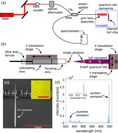
Light collection from the nanowire utilizes two GRIN lenses (Grintech GmbH) and a pig-tailed fibre (Nufern HI 1060). Emission from the nanowire is collimated with a 0.5 NA GRIN lens and re-focused into the fibre using a second lens with . The schematic of the GRIN assembly is shown in FIG. 1(b). For the GRIN lens assembly, we estimate, at 950 nm wavelength, 220 m for the free space focal length, and 0.76 m for the beam waist. This is predicted using one dimensional calculations with the transfer matrix method. Using a 965 nm laser, a CCD camera is used to directly measure the beam waist as a function of camera-lens separation in the far field. Using , the waist was found to be m, corresponding to a numerical aperture of . The system is designed for an NA that matches the divergence of the HE11 mode emitted from the tapered photonic nanowire waveguideDalacu, Williams, and Williams (2021) in order to provide a high mode overlap and near unity collection. The lens assembly is fixed together using an optically clear epoxy (EPO-TEK 301) and a glass ferrule sleeve.
Low temperature photoluminescence spectra of the quantum dot sample were take with the GRIN lenses in a closed-cycle He cryostat using the system arrangement seen in FIG. 1(a). The cryostat is equipped with three orthogonal piezoelectric-driven translation stages. The GRIN lens system is mounted on the stage whilst the sample is on the - stages. The system is optically pumped using a fibre-coupled laser source connected to the 1% arm of a 99:1 fused fibre power splitter and focused on the sample by the GRIN lenses. Reflected laser light and sample emission are collected by the lens assembly and directed along the 99% arm of the power splitter, towards a spectrometer equipped with a CCD detector array.
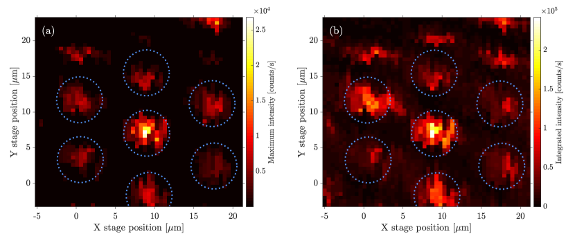
In lieu of conventional imaging, which is not possible using the GRIN lens assembly, we perform two dimensional (2D) scans of the sample surface using the - piezoelectric stage controllers. The scans are performed using a two stage process. We first find the focus () of the GRIN lens assembly by maximizing the reflected power from a 930 nm laser (similar to the dot emission wavelength). At this position the GRIN lens assembly is focused on the substrate which is sufficient to observe emission from both the quantum dot and the InP making up the photonic nanowire. The latter adopts a wurtzite crystal phase in our nanowires, with a higher bandgap (832 nm at 4 K) compared to bulk InP which has a zincblende crystal structure. In the second stage, we excite above band with wavelengths of 780 nm, 632 nm, or 670 nm and record the photoluminescence as a function of - position. A typical spectrum obtained when the GRIN lens assembly is over a nanowire is shown in FIG. 1(d), with both InAsP dot emission and wurtzite InP emission clearly visible.
Initial scans locate the nanowires on the substrate and we use these to adjust the -focus to optimize the collection of the quantum dot emission as opposed to focusing on the substrate. Examples of such in-focus scans can be seen in FIG. 2. The position step size used in the scans is 0.5 m in and , and the mode of travel of the piezoelectric drives is with slip-stick motion. Each of these coloured pixels is derived from a full spectrum measurement shown in FIG. 1(d). In FIG. 2(a), we take the maximum count rate in the expected spectral range of the quantum dot emission (908-950 nm) and in FIG. 2(b) we take a sum of the counts in the spectral range 823-836 nm which contains the peak associated with band to band recombination in the wurtzite InP nanowire. Comparison of the two figures highlights the spatial co-location of the dot and nanowire emission, important for room temperature alignment discussed later.
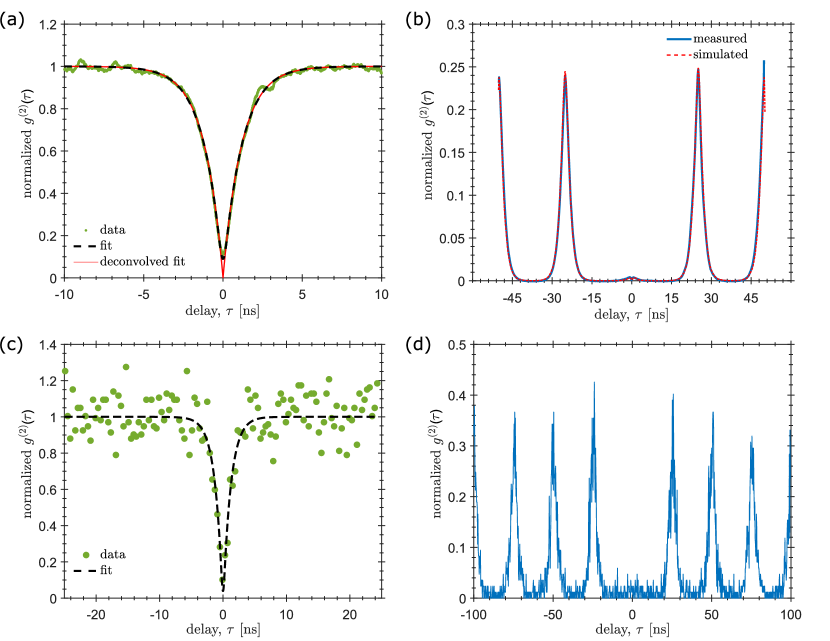
To determine the purity of the gathered single photons, measurements of the second order correlation function, were taken in a typical Hanbury Brown and Twiss (HBT) arrangement. We first optimize the position of the GRIN lens using the -- stages for maximum collection of emission from a chosen quantum dot. Count rates at saturation using continuous wave (CW) excitation are up to 1.4 Mcps. The bulk of the emission collected from the quantum dot will travel down the 99% arm of the first power splitter. A tunable narrowband transmission filter with a nm bandwidth suppresses dB of the out-of-band transmitted signal, including the laser pump power and unwanted sample emission. The filtered signal is fed into a 50:50 fused fibre power splitter with each 50% arm of the splitter leading to a single-photon avalanche diode (SPAD) detector. The signals from the detectors are time-correlated using counting electronics to build a histogram of the delay times between detection events on the first and second detector, .

FIG 3(a) shows a CW measurement made using a HeNe laser as an above-band excitation source. Assuming the CW without the effect of detectors is given by a Laplace distribution and that the detector response can be described by a gaussian, the normalized second order correlation measurement seen in the experiment is given by
| (1) |
where is defined as
where is the radiative recombination rate of the excitonic complex, is the detector jitter, and describes the magnitude of the correlation minimum. The SPADs used in these measurements have a detection jitter of ps. The expected time-correlated response without the influence of detectors is also plotted against the experimental data. This curve is produced by taking the fit to the correlation data and plotting it again with .
In FIG 3(b) we demonstrate on-demand operation using a diode laser (emitting at 670 nm) as a pulsed excitation source. Pumping at saturation using 39 ps pulses repeated at 40 MHz, we obtain a total count rate at the detectors of 0.2 Mcps. At this pump power, the measured (i.e. the normalized area of the peak). The same value was obtained by fitting the curve using a stochastic model to simulate the pulsed HBT experimentDalacu et al. (2020). The high single photon purity, even at saturation and using above-band excitation, is a consequence of the deterministic growth process employed in the manufacture of the source, which produces devices containing one and only one emitter.
To estimate the device efficiency, we account for the throughput of all the fibre components (20%) and the detector efficiency (25%) from which we estimate 4 Mcps single photons coupled into the fibre by the GRIN lens. Considering the excitation pulse repetition rate of 40 MHz, and assuming the quantum efficiency for the quantum dot is 100%, this corresponds to 10% of the photons emitted by the dot being coupled into the fibre. To estimate the collection efficiency of the GRIN lens system itself we have to take into account the fact that not all the photons emitted by the dot will be radiated from the top of the nanowire. We assume a loss of 50% for photons emitted by the dot that are directed down towards the substrate and 5% into radiation modes (i.e. . We also have to take into account 25% which emit from a different charge state (see Fig. 1(c)) and 20% that emit into the phonon sidebands, both of which are filtered out. These loss channels reduce the maximum number of the desired photons at the input of the GRIN lens to 28.5% of 40 MHz. Accordingly, we estimate a GRIN lens assembly collection efficiency of 35%.
We speculate that the large fraction of uncollected photons (65%) is due to imperfect alignment, in particular, a tilt of the GRIN lens system with respect to the substrate. In a separate experiment, we have measured the dependence of the coupling efficiency on the deviation of the GRIN lens axis from the substrate normal and have observed a decrease of over 50% at angles as small as 1∘. Angle alignment can be readily improved by incorporating precise pitch and yaw control during the alignment process. We also note that nanowire device designs exist that can reduce some of non-alignment related sources of loss, including the incorporation of a back mirrorClaudon et al. (2010); Reimer et al. (2012) and charge-state controlZeeshan et al. (2019).
We turn next to room temperature alignment and PnP operation. We focus a 930 nm laser onto the surface looking at the reflected laser power, as before, but here, we also perform an - scan which provides information on the surface topography. An example is shown in FIG. 4(b) where the target array of nanowires is clearly visible. While knowing the location of nanowires using reflected laser power can give a rough stage location for GRIN lens-nanowire coupling, it is not suitable for determining if the lens is in the proper focus position to maximize quantum dot emission collection. To better position the fibre and lenses, we investigated whether room temperature wurtzite InP emission scans were possible. In FIG. 4(c), such a scan shows that wurtzite InP emission can clearly show distinct nanowires, allowing for precise positioning of the collection lenses at room temperature. An optical image of the same nanowire array [Fig. 4(a)] shows that the emission image accurately recreates the same arrangement of nanowires, where missing wires are seen in the same locations in both images.
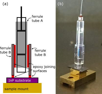
To permanently fix the alignment of the nanowire to the fibre assembly we first fix the nanowire growth substrate onto the metal sample holder using 3M 2216 B/A epoxy adhesive. An outer ferrule tube (B in FIG. 5(a)) is placed, loose, on top of the InP substrate, located roughly above a target array of nanowires. The GRIN lens assembly used in the low temperature measurements (A in FIG. 5(a)) is then lowered into the outer ferrule tube. Using a 930 nm laser, the GRIN lens assembly is brought into focus on the substrate surface using the reflected intensity to optimize – this focus position is typically a few microns below the ideal focus position for quantum dot emission. The GRIN lens assembly (A) is now glued to the inner walls of the outer ferrule tube (B) using EPO-TEK 301-2 epoxy and cured for approximately 3 hours at 75∘C. After curing, the assembly is raised a few microns and a small - scan is performed to locate a chosen nanowire using the wurtzite InP emission. Once located, the optimum focus is found and the outer ferrule tube is glued to the substrate using EPO-TEK 301-2 epoxy and further cured at 75∘C for another 3 hours. A picture of the finished device is shown in FIG. 5(b).
The device was then cooled to 4 K and operated as a PnP source. Measured count rates were cps, significantly lower compared to devices employing active alignment at low temperature, but single photon purity remained high, with , see FIG. 3(c), (d). This initial device was intended to verify the feasibility of the approach, and, in particular, the alignment stability. No variation in count rate was observed after several cool-downs in the cryostat, nor was any observed after several immersions in liquid N2.
To increase the count rate to the levels achieved using active low temperature alignment, more careful attention to the chosen focus position at which the GRIN lens is fixed is required. In a separate experiment we found that the focus position for optimal collection of the InP emission occurs a few microns below that of the quantum dot emission. This misalignment in the focus that occurs with room temperature InP emission alignment can be readily calibrated out. Another interesting avenue is to apply the technique to telecom nanowire quantum dot emittersHaffouz et al. (2018). The quantum dots used in these sources have a deeper confining potential and emit brightly even at room temperatureFiset-Cyr et al. (2018). Consequently, emission from the dots themselves can be used for alignment instead of the InP nanowire emission.
In summary, we demonstrate a process to efficiently couple single photons from InAsP quantum dots embedded in InP photonic nanowire waveguides into a single mode fibre using a compact and robust GRIN lens assembly. The collection efficiency of the GRIN lens system (e.g. fraction of the single photons directed towards the lens assembly that were collected) was 35% whilst the overall single photon collection efficiency (fraction of the total single photons produced by the quantum dot that were collected) was 10%. We also describe a manufacturing method to produce high purity single photon sources that can be operated in a “plug and play" mode. The method is based on active alignment using the emission of the InP nanowire in which the InAsP quantum dot is embedded. This alignment can be performed at room temperature, where the fibre can be permanently attached to the chip.
Acknowledgements.
This work was supported by the Canadian Space Agency through a collaborative project entitled ‘Development of Quantum Dot Based QKD-relevant Light Sources’References
- O’Brien, Furusawa, and Vučković (2009) J. L. O’Brien, A. Furusawa, and J. Vučković, “Photonic quantum technologies,” Nat. Photon. 3, 687 (2009).
- Gazzano et al. (2013) O. Gazzano, M. P. Almeida, A. K. Nowak, S. L. Portalupi, A. Lemaître, I. Sagnes, A. G. White, and P. Senellart, “Entangling quantum-logic gate operated with an ultrabright semiconductor single-photon source,” Phys. Rev. Lett. 110, 250501 (2013).
- Bulgarini et al. (2014) G. Bulgarini, M. E. Reimer, M. B. Bavinck, K. D. Jöns, D. Dalacu, P. J. Poole, E. P. A. M. Bakkers, and V. Zwiller, “Nanowire waveguides launching single photons in a gaussian mode for ideal fiber coupling,” Nano Lett. 7, 4102–4106 (2014).
- Lee et al. (2021) C.-M. Lee, M. A. Buyukkaya, S. Harper, S. Aghaeimeibodi, C. J. K. Richardson, and E. Waks, “Bright telecom-wavelength single photons based on a tapered nanobeam,” Nano Lett. 21, 323 (2021).
- Muller et al. (2009) A. Muller, E. B. Flagg, M. Metcalfe, J. Lawall, and G. Solomon, “Coupling an epitaxial quantum dot to a fiber based external-mirror microcavity,” Appl. Phys. Lett. 95, 173101 (2009).
- Greuter et al. (2015) L. Greuter, S. Starosielec, A. V. Kuhlmann, and R. J. Warburton, “Towards high-cooperativity strong coupling of a quantum dot in a tunable microcavity,” Phys. Rev. B 92, 045302 (2015).
- Fujiwara et al. (2011) M. Fujiwara, K. Toubaru, T. Noda, H.-Q. Zhao, and S. Takeuchi, “Highly efficient coupling of photons from nanoemitters into single-mode optical fibers,” Nano Lett. 11, 4362 (2011).
- Liebermeister et al. (2014) L. Liebermeister, F. Petersen, D. B. Asmus v. Münchow, J. Hermelbracht, T. Tashima, A. W. Schell, O. Benson, T. Meinhardt, A. Krueger, A. Stiebeiner, A. Rauschenbeutel, H. Weinfurter, and M. Weber, “Tapered fiber coupling of single photons emitted by a deterministically positioned single nitrogen vacancy center,” Appl. Phys. Lett. 104, 031101 (2014).
- Ates et al. (2013) S. Ates, I. Agha, A. Gulinatti, I. Rech, A. Badolato, and K. Srinivasan, “Improving the performance of bright quantum dot single photon sources using temporal filtering via amplitude modulation,” Sci. Rep. 3, 1397 (2013).
- Lee et al. (2015) C.-M. Lee, H.-J. Lim, C. Schneider, S. Maier, S. Höfling, M. Kamp, and Y.-H. Lee, “Efficient single photon source based on -fibre-coupled tunable microcavity,” Sci. Rep. 5, 14309 (2015).
- Patel et al. (2016) R. N. Patel, T. Schröder, N. Wan, L. Li, S. L. Mouradian, E. H. Chen, and D. R. Englund, “Efficient photon coupling from a diamond nitrogen vacancy center by integration with silica fiber,” Light: Science & Applications 5, e16032 (2016).
- Daveau et al. (2017) R. S. Daveau, K. C. Balram, T. Pregnolato, J. Liu, E. H. Lee, J. D. Song, V. Verma, R. Mirin, S. W. Nam, L. Midolo, S. Stobbe, K. Srinivasan, and P. Lodahl, “Efficient fiber-coupled single-photon source based on quantum dots in a photonic-crystal waveguide,” Optica (2017).
- Burek et al. (2017) M. J. Burek, C. Meuwlyk, R. E. Evansk, M. K. Bhaskark, A. Sipahigilk, S. Meesalak, B. Machielsek, D. D. Sukachevk, C. T. Nguyenk, J. L. Pachecok, E. Bielejeck, M. D. Lukink, and M. Lončar1, “Fiber-coupled diamond quantum nanophotonic interface,” Physl Rev. Appl. 8, 024026 (2017).
- Xu et al. (2007) X. Xu, I. Toft, R. T. Phillips, J. Mar, K. Hammura, and D. A. Williams, ““plug and play” single-photon sources,” Appl. Phys. Lett. 90, 061103 (2007).
- Xu et al. (2014) X. Xu, F. Brossard, K. Hammura, D. A. Williams, B. Alloing, L. H. Li, and A. Fiore, ““plug and play” single photons at 1.3 m approaching gigahertz operation,” Appl. Phys. Lett. 93, 021124 (2014).
- Ma et al. (2017) B. Ma, Z.-S. Chen, S.-H. Wei, X.-J. Shang, H.-Q. Ni, and Z.-C. Niu, “Single photon extraction from self-assembled quantum dots via stable fiber array coupling,” Appl. Phys. Lett. 110, 142104 (2017).
- Żołnacz et al. (2019) K. Żołnacz, A. Musiał, N. Srocka, J. Große, M. J. Schlösinger, P.-I. Schneider, O. Kravets, M. Mikulicz, J. Olszewski, K. Poturaj, G. Wójcik, P. Mergo, K. Dybka, M. Dyrkacz, M. Dłubek, S. Rodt, S. Burger, L. Zschiedrich, G. Sęk, S. Reitzenstein, and W. Urbańczyk, “Method for direct coupling of a semiconductor quantum dot to an optical fiber for single-photon source applications,” Optics Express 27, 26772–26785 (2019).
- Schlehahn et al. (2018) A. Schlehahn, S. Fischbach, R. Schmidt, A. Kaganskiy, A. Strittmatter, S. Rodt, T. Heindel, and S. Reitzenstein, “A stand-alone fiber-coupled single-photon source,” Sci. Rep. 8, 1340 (2018).
- Bremer et al. (2020) L. Bremer, K. Weber, S. Fischbach, S. Thiele, M. Schmidt, A. Kaganskiy, S. Rodt, A. Herkommer, M. Sartison, S. L. Portalupi, P. Michler, H. Giessen, , and S. Reitzenstein, “Quantum dot single-photon emission coupled into single-mode fibers with 3d printed micro-objectives,” APL Photon. 5, 106101 (2020).
- Haupt et al. (2010) F. Haupt, S. S. R. Oemrawsingh, S. M. Thon, H. Kim, D. Kleckner, D. Ding, D. J. Suntrup, P. M. Petroff, and D. Bouwmeester, “Fiber-connectorized micropillar cavities,” Appl. Phys. Lett. 97, 131113 (2010).
- Snijders et al. (2018) H. Snijders, J. A. Frey, J. Norman, V. P. Post, A. C. Gossard, J. E. Bowers, M. P. van Exter, W. L offler, and D. Bouwmeester, “Fiber-coupled cavity-qed source of identical single photons,” Phys. Rev. Appl. 9, 031002 (2018).
- Schroder et al. (2011) T. Schroder, A. W. Schel, G. Kewes, T. Aichele, and O. Benson, “Fiber-integrated diamond-based single photon source,” Nano Lett. 11, 198 (2011).
- Vogl, Lu, and Lam (2017) T. Vogl, Y. Lu, and P. K. Lam, “Room temperature single photon source using fiber-integrated hexagonal boron nitride,” J. Phys. D: Appl. Phys. 50, 295101 (2017).
- Sasakura et al. (2013) H. Sasakura, X. Liu, S. Odashima, H. Kumano, S. Muto, and I. Suemune, “Fiber-based bidirectional solid-state single-photon emitter based on semiconductor quantum dot,” Appl. Phys. Express 6, 065203 (2013).
- Zha et al. (2015) G.-W. Zha, X.-J. Shang, H.-Q. Ni, Y. Yu, J.-X. Xu, S.-H. Wei, B. Ma, L.-C. Zhang, and Z.-C. Niu, “In situ probing and integration of single self-assembled quantum dots-in-nanowires for quantum photonics,” Nanotechnology (2015), 10.1088/0957-4484/26/38/385706.
- Cadeddu et al. (2016) D. Cadeddu, J. Teissier, F. R. Braakman, N. Gregersen, P. Stepanov, J.-M. Gérard, J. Claudon, R. J. Warburton, M. Poggio, and M. Munsch, “A fiber-coupled quantum-dot on a photonic tip,” Appl. Phys. Lett. 108, 011112 (2016).
- Lee et al. (2019) C.-M. Lee, M. A. Buyukkaya, S. Aghaeimeibodi, A. Karasahin, C. J. K. Richardson, and E. Waks, “A fiber-integrated nanobeam single photon source emitting at telecom wavelengths,” Applied Physics Letters 114, 171101 (2019).
- Dalacu, Poole, and Williams (2019) D. Dalacu, P. J. Poole, and R. L. Williams, “Nanowire-based sources of non-classical light,” Nanotechnology 30, 232001 (2019).
- Reimer et al. (2016) M. E. Reimer, G. Bulgarini, A. Fognini, R. W. Heeres, B. J. Witek, M. A. M. Versteegh, A. Rubino, T. Braun, M. Kamp, S. Höfling, D. Dalacu, J. Lapointe, P. J. Poole, and V. Zwiller, “Overcoming power broadening of the quantum dot emission in a pure wurtzite nanowire,” Phys. Rev. B 93, 195316 (2016).
- Claudon et al. (2010) J. Claudon, J. Bleuse, N. S. Malik, M. Bazin, P. Jaffrennou, N. Gregersen, C. Sauvan, P. Lalanne, and J.-M. Gérard, “A highly efficient single-photon source based on a quantum dot in a photonic nanowire,” Nat. Photon. 4, 174 (2010).
- Dalacu et al. (2009) D. Dalacu, A. Kam, D. G. Austing, X. Wu, J. Lapointe, G. C. Aers, and P. J. Poole, “Selective-area vapour-liquid-solid growth of inp nanowires,” Nanotech. 20, 395602 (2009).
- Dalacu et al. (2011) D. Dalacu, K. Mnaymneh, X. Wu, J. Lapointe, G. C. Aers, P. J. Poole, and R. L. Williams, “Selective-area vapor-liquid-sold growth of tunable inasp quantum dots in nanowires,” Appl. Phys. Lett. 98, 251101 (2011).
- Dalacu, Williams, and Williams (2021) D. Dalacu, P. J. Williams, and R. L. Williams, “Tailoring the geometry of bottom-up nanowires: Application to high efficiency single photon sources,” submitted Nano Mater. (2021).
- Dalacu et al. (2020) D. Dalacu, D. B. Northeast, P. J. Poole, G. C. Aers, R. L. Williams, K. A. Owen, and D. Oblak, “Pump power control of photon statistics in a nanowire quantum dot,” Phys. Rev. B 102, 115401 (2020).
- Reimer et al. (2012) M. E. Reimer, G. Bulgarini, N. Akopian, M. Hocevar, M. B. Bavinck, M. A. Verheijen, E. P. A. M. Bakkers, L. P. Kouwenhoven, and V. Zwiller, “Bright single-photon sources in bottom-up tailored nanowires,” Nat. Commun. 3, 737 (2012).
- Zeeshan et al. (2019) M. Zeeshan, N. Sherlekar, A. Ahmadi, R. L. Williams, and M. E. Reime, “Proposed scheme to generate bright entangled photon pairs by application of a quadrupole field to a single quantum dot,” Phys. Rev. Lett. 122, 227401 (2019).
- Haffouz et al. (2018) S. Haffouz, K. D. Zeuner, D. Dalacu, P. J. Poole, J. Lapointe, D. Poitras, K. Mnaymneh, X. Wu, M. Couillard, M. Korkusinski, E. Schöll, K. D. Jöns, V. Zwiller, and R. L. Williams, “Bright single inasp quantum dots at telecom wavelengths in position-controlled inp nanowires: The role of the photonic waveguide,” Nano Lett. 18, 3047 (2018).
- Fiset-Cyr et al. (2018) A. Fiset-Cyr, D. Dalacu, S. Haffouz, P. J. Poole, J. Lapointe, G. C. Aers, and R. L. Williams, “In-situ tuning of individual position-controlled nanowire quantum dots via laser-induced intermixing,” Appl. Phys. Lett. 113, 053105 (2018).