A Composable Glitch-Aware Delay Model ††thanks: This research was partially funded by the Austrian Science Fund (FWF) projects DMAC (P32431) and ADynNet (P28182), the Centre National de la Recheche Scientifique projects ABIDE and BACON, the Agence Nationale de la Recherche project FREDDA (ANR-17-CE40-0013), and by the DigiCosme working group HicDiesMeus under ANR grant agreements ANR-11-LABEX-0045-DIGICOSME and ANR-11-IDEX-0003-02
Abstract
We introduce the Composable Involution Delay Model (CIDM) for fast and accurate digital simulation. It is based on the Involution Delay Model (IDM) [Függer et al., IEEE TCAD 2020], which has been shown to be the only existing candidate for faithful glitch propagation known so far. In its present form, however, it has shortcomings that limit its practical applicability and utility. First, IDM delay predictions are conceptually based on discretizing the analog signal waveforms using specific matching input and output discretization threshold voltages. Unfortunately, they are difficult to determine and typically different for interconnected gates. Second, metastability and high-frequency oscillations in a real circuit could be invisible in the IDM signal predictions. Our CIDM reduces the characterization effort by allowing independent discretization thresholds, improves composability and increases the modeling power by exposing canceled pulse trains at the gate interconnect. We formally show that, despite these improvements, the CIDM still retains the IDM’s faithfulness, which is a consequence of the mathematical properties of involution delay functions.
Index Terms:
digital timing simulation; composable delay estimation model; faithful glitch propagation; pulse degradationI Introduction and Context
Accurate prediction of signal propagation is a crucial task in modern digital circuit design. Although the highest precision is obtained by analog simulations, e.g., using SPICE, they suffer from excessive simulation times. Digital timing analysis techniques, which rely on (i) discretizing the analog waveform at certain thresholds and (ii) simplified interconnect resp. gate delay models, are hence utilized to verify most parts of a circuit. Prominent examples of the latter are pure (constant input-to-output delay ) and inertial delays (constant delay , pulses shorter than an upper bound are removed) [1]. To accurately determine , which stays constant for all simulation runs, highly elaborate estimation methods like CCSM [2] and ECSM [3] are required.
Single-history delay models, like the Degradation Delay Model (DDM) [4], have been proposed as a more accurate alternative. Here, the input-to-output delay depends on a single parameter, the previous-output-to-input delay (see Fig. 1). Still, Függer et al. [5] showed that none of the existing delay models, including DDM, is faithful, as they fail to correctly predict the behavior of circuits solving the canonical short-pulse filtration (SPF) problem.
Függer et al. [7] introduced the Involution Delay Model (IDM) and showed that, unlike all other digital delay models known so far, it faithfully models glitch propagation. The distinguishing property of the IDM is that the delay functions for rising () and falling () transitions form an involution, i.e., . A simulation framework based on ModelSim, the Involution Tool, confirmed the accuracy of the model predictions for several simple circuits [8].
Nevertheless, the IDM shows, at the moment, several shortcomings which impair its composability:
(I) Ensuring the involution property requires specific (“matching”) discretization threshold voltages and to discretize the analog waveforms at in- and output. These are not only unique for every single gate in the circuit but also difficult to determine. (II) The discretization threshold voltages may vary from gate to gate, i.e., the matching output discretization threshold voltage of a given gate and the matching input discretization threshold voltage of a successor gate are not necessarily the same. Consequently, just adding the delay predictions of the IDM for and cannot be expected to accurately model the overall delay of their composition. This is particularly true for circuits designs where different transistor threshold voltages [9] are used for tuning the delay-power trade-off [10] or reliability [11].
(III) Intermediate voltages, caused by creeping or oscillatory metastability, are expressed differently for various values of : Ultimately, a single analog trajectory may result in either zero, one or a whole train of digital transitions.
Main contributions:
In the present paper, we address all these shortcomings.
-
1)
Based on the empirical analysis of the impact of and on the delay functions of a real circuit, we introduce CIDM channels, which are essentially made up of a typically asymmetric (for rising/falling transitions) pure delay shifter followed by an IDM channel (a PI channel). CIDM channels can model gates with arbitrarily discretization threshold and and simplify the characterization of their delay functions. Moreover, the CIDM exposes cancellations at the interconnect between gates, rather than removing them silently as in the IDM. Consequently, digital timing simulators can, for example, record trains of canceled pulses and report it to the user accordingly.
-
2)
We prove that CIDM channels are not equivalent to IDM channels per se, in the sense that their delay functions are not involutions. However, the fact that both essentially contain the same components allows us to map a CIDM circuit description to an IDM one: For every circuit modeled with compatible CIDM channels, modeling matching discretization threshold voltages, there is an equivalent decomposition into IP channels, consisting of an IDM channel followed by an arbitrary pure delay shifter. Somewhat surprisingly, the mathematical properties of involution delay functions reveal that IP channels are instances of IDM channels. Consequently, the faithfulness of the IDM carries over literally to the CIDM.
-
3)
We present the theoretical foundations and an implementation of a simulation framework for CIDM, which was incorporated into the Involution Tool [8]. 111The original Involution Tool is accessible via https://github.com/oehlinscher/InvolutionTool, our extended version is provided at https://github.com/oehlinscher/CDMTool. We also provide a proof of correctness of our simulation algorithm, which shows that it always terminates after having produced the unique execution of an arbitrary circuit composed of gates with compatible CIDM channels.
-
(4)
We conducted a suite of experiments, both on a custom inverter chain with varying matching threshold voltages and a standard inverter chain. In the former case, we observed an impressive improvement of modeling accuracy for CIDM over IDM in many cases.
Paper organization: We start with some basic properties of the existing IDM in Section II. In Section III, we empirically analyze the impact of changing and on the delay functions. Section IV introduces and justifies the CIDM, while Section V proves its faithfulness. In Section VI, we describe the CIDM simulation algorithm and its implementation, and prove that its correctness. Section VII provides the results of our experiments. Some conclusion in Section VIII round-off our paper.
II Involution Delay Model Basics
In this section, we briefly discuss the IDM. For further details, the interested reader is referred to the original publication [7].
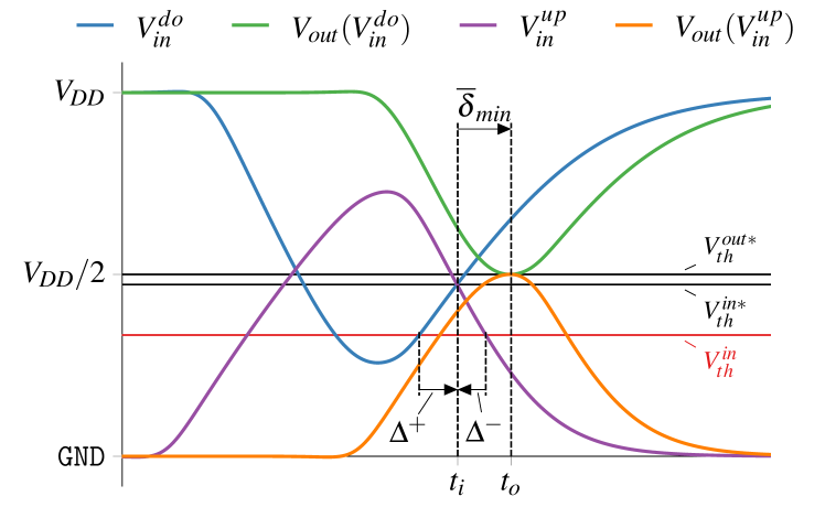
The essential benefit of using delay functions which are involutions is their ability to perfectly cancel zero-time input glitches: In Fig. 1, it is apparent that the rising input transition causes a rising transition at the output, after delay . Now suppose that there is an additional falling input transition immediately after the rising one, actually occurring at the same time. Since this constitutes a zero-time input glitch, which is almost equivalent to no pulse at all, the output should behave as if it was not there at all.
For this purpose it is required that the delay of the additional falling input transition to go back in time, i.e., to exactly hit the predicted time of the previous falling output transition: Note carefully that just canceling the rising output transition, by generating the falling output transition at or before the rising one, would not suffice, as the calculation of the parameter for the next transition depends on the time of the previous output transition. It is not difficult to check that this going back is indeed achieved when and holds. As the IDM also requires the delay functions to be strictly increasing and concave, the involution property enforces them to be symmetric w.r.t. the 2nd median .
Lemma 3 in [7], restated as Lemma 1 below, shows that strictly causal involution channels, characterized by strictly increasing, concave delay functions with and , give raise to a unique that (i) resides on the 2nd median and (ii) is shared by and due to the involution property.
Lemma 1 ([7, Lem. 3]).
A strictly causal involution channel has a unique defined by .
In [7], Függer et al. have shown that self-inverse delay functions arise naturally in a (generalized) standard analog model that consists of a pure delay, a slew-rate limiter with generalized switching waveforms and an ideal comparator (see Fig. 2). First, the binary-valued input is delayed by , which assures causal channels, i.e., . For every transition on , the generalized slew-rate limiter switches to the corresponding waveform ( for a falling/rising transition). Note that the value at (the analog output voltage) does not jump, i.e., is a continuous function. Finally, the comparator generates the output by discretizing the value of this waveform w.r.t. the discretization threshold .
Using this representation, the need for can be explained by the necessity to cover sub-threshold pulses, i.e., ones that do not reach the output discretization threshold. In this case, the switching waveform has to be followed into the past to cross , resulting in the seemingly acausal behavior.
III Discretization Threshold Voltages
In this section, we will empirically explore the relation of gate delays and discretization threshold voltages by means of simulation results.222Our simulations have been performed for a buffer in the NanGate library. However, since we are only reasoning about qualitative aspects common to all technologies, the actual choice has no significance. In most of the following observations, we assume that a given physical (analog) gate is to be characterized as a zero-time Boolean gate with a succeeding IDM channel that models the delay. In order to accomplish concrete values, discretization threshold voltages at the input and at the output of a gate have to be fixed, and the pure delay component of the IDM channel as well as the delay functions and are determined accordingly.
Definition 2.
The input and output discretization voltages and are called matching for a gate, if the induced delay functions , fulfill the condition . To stress that a pair of input and output discretization threshold voltages is matching, they will be denoted as and .
We will now characterize properties of matching discretization threshold voltages. They depend on many factors, including transistor threshold voltages [9] and the symmetry of the pMOS vs. nMOS stack. Since varying these parameters is commonly used in advanced circuit design to trade delay for power consumption [10, 12] and reliability [11], as well as for implementing special gates (e.g. logic-level conversion [13]), the range of suitable discretization threshold voltages could differ significantly among gates.
Considering these circumstances it seems impossible that output and input descretization values coincide among connected gates. However, the following observation shows that there is an unlimited number of matching discretization threshold pairs for IDM:
Observation 3.
For every choice of , there is exactly one matching . Fixing either of them uniquely determines the other and, in addition, also the pure delay .
Justification.
Let us fix and investigate how and can be determined. For this purpose, we consider an analog pulse at that barely touches , i.e., results in a zero-time glitch in the digital domain. There is a unique positive and a unique negative analog output pulse with this shape, which is both confirmed by simulation results and analytic considerations on the underlying system of differential equations [14]. Now shift the positive and negative pulses in time such that their output voltages touch , one from below and the other from above, at time (see Fig. 3). Due to the condition , this implies that the falling transition of the positive pulse and the rising transition of the negative pulse at the input must both cross at time . Thus, fixing uniquely determines the matching and . ∎
Actually determining the matching for a given and vice versa is a challenging task. For a start, let us investigate the static case with being the static transfer function of a gate. In this setup, an output derivative is achieved for all values fulfilling the condition since represents the stable states of the gate. To obtain high accuracy when discretizing the analog signal, one typically chooses the output threshold such that the respective output waveform for a full-range input pulse has a steep slope at this point. While is in general a good choice, the corresponding will differ significantly between balanced and high-threshold inverters, for example.
Besides these static considerations, for a dynamic input, coupling capacitances cause a current at the output, which must be compensated via the gate-source voltages of the transistors as well. Obviously, the required overshoot w.r.t. , and hence the time until this value is reached, depends on many parameters like the size of the coupling capacitances and the slope of the input signal.
It is also worth mentioning that CMOS logic shows an inverse proportionality between in- and output, i.e., increasing the input increases the conductivity to GND, which drains the output, and vice versa. This implies that the current induced by the alternation of the input goes against the change of the output current, which effectively slows down the switching operation, and thus increases the pure delay .
3 has a severe consequence for the simulation of circuits in any model, like IDM, where Lemma 1 holds:
Observation 4.
Fixing either or for a single gate fixes the threshold voltages of all gates in the circuit when it is simulated in a model where 3 holds.
Justification.
For a single gate, the observation follows from the unique relationship between and by 3. For gates in a path, the ability to just add up their delays requires output and next input discretization thresholds to be the same. ∎
Since the detailed relation of and according to 3 depends on the individual gate, this means that the discretization threshold voltages across a circuit may vary in a priori arbitrary ways, depending on the interconnect topology and the gate properties. In the extreme, the discretization thresholds can exceed the acceptable range for some gates, and even lead to unsatisfiable assignments in the case of circuits containing feedback-loops. In any case, it may take a large effort to properly characterize every gate such that the dependencies among discretization thresholds are fulfilled. By contrast, an ideally composable delay model uses a uniform discretization threshold such as .
To investigate if IDM allows such a uniform choice, we proceed with 5:
Observation 5.
Characterizing a gate with non-matching discretization thresholds and , where matching and lead to an IDM channel with pure delay , results in delay functions , , which satisfy and for . and have opposite sign, with for .
Justification.
The observation follows from refining the argument used for confirming 3, where it was shown how matching and are achieved. For the non-matching case, we increase resp. decrease , starting from , while keeping everything else, i.e., electronic characteristics, waveforms and , unchanged. As illustrated in Fig. 3 for , it still takes from hitting (at time ) to seeing a zero time glitch (at time ) at the output. The falling transition has already crossed when it hits on , whereas the rising transition still has some way to go: Denoting the switching waveforms of the preceding gate (driving the input) by and , the pure delay for the rising resp. falling transition evaluates to and with
| (1) |
Consequently, and indeed holds. Finally, since must obviously rise and must fall, it follows that if (the case in Fig. 3) then . ∎
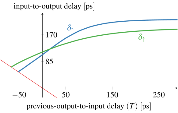
Fig. 4 shows the derived delay function for non-matching discretization thresholds. Clearly visible are the different pure delays . Please note, that in our justification of 5, we focused on and how it changes with varying discretization threshold voltages. If the rising and falling switching waveforms were always the same, as is assumed in the analog channel model Fig. 2, this would result in delay functions that are fixed in shape and are simply shifted along the 2nd median. The actual delay functions of gates, obtained by analog simulations, for example, exhibit additional deviations (for ), however, since the shape of the input switching waveforms also vary. Consequently, the difference between and will not always be passed in constant time.
Finally, the dependency of the IDM on the particular choice of the discretization threshold voltages also reveals a different problem:
Observation 6.
Different choices of can significantly change the digital model prediction of the IDM.
Justification.
Sub-threshold pulses are automatically removed by the comparator in Fig. 2, i.e., they are completely invisible in the digital signal that is fed to the successor gate. Consequently analog traces, that do not cross , e.g., high-frequency oscillations at intermediate voltage levels, may be totally suppressed: Assume an oscillatory behavior of a gate output with minimal voltage and maximal . These oscillations would only be reflected in the digital discretization if . ∎
IV Composable Involution Delays
In this section, we define our Composable Involution Delay Model (CIDM), which allows to circumvent the problems presented in the previous section: According to 5, using non-matching thresholds introduces a pure delay shift. The major building blocks of our CIDM are hence PI channels, which consist of a pure delay shifter with different shifts and for rising and falling transitions 333A pure delay shifter with causes a constant extension/compression of up/down input pulses by . followed by an IDM channel. In order to also alleviate the problem of invisible oscillations identified in 6, we re-shuffle the internal architecture of the original involution channels shown in Fig. 2 in order to expose trains of canceled transitions on the interconnecting wires.
Theorem 7 (PI channel properties).
Consider a channel PI formed by the concatenation of a pure delay shifter with followed by an involution channel , given via and with minimum delay . Then PI is not an involution channel, but rather characterized by delay functions defined as
| (2) |
These functions satisfy
| (3) | ||||
| (4) | ||||
| (5) | ||||
| (6) |
for and .
Proof.
Consider an input signal consisting of a simple negative pulse, as depicted in Fig. 1. Let resp. be the time of the falling resp. rising input transition, resp. the time of the falling resp. rising transition at the output of the pure delay shifter, and resp. the time of the falling resp. rising transition after the involution channel. With , we get as well as and .
For the delay function of the PI channel, if we set , we find
| (7) |
as asserted. By setting and using the equality is achieved, which confirms 5.
By analogous reasoning for an up-pulse at the input, which results in the same equations as above with exchanged with and with , we also get
| (8) |
as asserted. Setting and using confirms 6 as well.
Using a simple parameter substitution allows to transform 7 and 8 to
| (9) | ||||
| (10) |
Utilizing these in the involution property of and provides
If we substitute in the last line, we arrive at
| (11) |
which confirms 3.
Doing the same for the reversed involution property of , provides
If we substitute in the last line, we arrive at
| (12) |
which confirms 4.
∎
Eq. 2 implies that resp. are the result of shifting resp. along the 2nd median by resp. . It is apparent from Fig. 4, though, that the choice of , cannot be arbitrary, as it restricts the range of feasible values for via the domain of resp. (see Definition 10 for further details).
This becomes even more apparent in the analog channel model. Fig. 5 (a) shows an extended block diagram of an IDM channel where we applied two changes: First, we added a (one-input, one-output) zero-time Boolean gate . Second, we split the comparator at the end into a thresholder and a cancellation unit . The thresholder unit outputs, for each transition on , a corresponding -crossing time of , independently of whether it will actually be reached or not. For subthreshold pulses, the transition might even be scheduled in the past. The cancellation unit only propagates transitions that are in the correct temporal order. The components and together implement the same functionality as a comparator.
At the beginning of the channel, the Boolean gate (we assume a single-input gate for now) evaluates the input signal in zero time and outputs , which is subsequently delayed by the pure delay shifter . Here lies the cause of the problem: If either or it is possible that transitions are in reversed temporal order which, after being delayed by the constant pure delay , have to be processed in this fashion by the slope delimiter. The latter is, however, only defined on traces encoded via the alternating Boolean signal transitions’ Waveform Switching Times (WST), which occur in a strictly increasing temporal order and mark the points in time when the switching waveforms shall be changed. Placing the delay shifter in front of the gate, as shown in Fig. 5 (b), does not change the situation, since the gate also expects transitions in the correct temporal order (note that this is not equal to WST since the pure delay is still missing).
One possibility to avoid transitions in the wrong temporal order at the Boolean gate is to move the canceling unit to the front, as shown in Fig. 5 (c). This solves our present problems but has the consequence, that now transitions are interchanged among gates using the Threshold Crossing Times (TCT) encoding: The TCT encoding gives, in sequence order, the points in time when the analog switching waveform would have crossed (it is not required that it actually does). Consequently, a signal given in TCT also exposes canceled transitions. Actually this is very convenient for us, since this allows us implicitly to detect oscillations independent of the chosen output threshold and thus solves design challenge (3) from the introduction.
Not all signals in Fig. 5 can actually be mapped to TCT or WST; by suitably recombining the components in our CIDM channel, however, these encodings will be sufficient for our purposes. More specifically, TCT will be created by the scheduler , subsequently modified by the delay shifter, altered by the cancellation unit , evaluated by the Boolean gate and finally transformed to WST by .
Now we are finally ready to formally define a CIDM channel (see Fig. 6). Note that, although a PI channel differs by its internal structure significantly from the CIDM channel, they are equivalent with respect to Theorem 7.
Definition 8.
A CIDM channel comprises in succession of a pure delay shifter, a cancellation unit, a Boolean gate, a pure-delay unit, a shaping unit and a thresholding unit [see Fig. 5(c)].
One may wonder whether CIDM channels could be partitioned also in a different fashion. The answer is yes, several other partitions are possible. For example, one could transmit signal and move the slew-rate limiter and the scheduler to the succeeding channel. This would, however, mean that properties of single CIDM channels depend on the properties of both predecessor and successor gate, which complicates the process of channel characterization and parametrization based on design parameters.
The main practical advantage of a CIDM channel, which is a generalization of an IDM channel (just set ), is the additional degree of freedom for gate characterization in conjunction with the fact that a single channel encapsulates a single gate.
V Glitch Propagation in the CIDM
Since CIDM channels do not satisfy the involution property, the question about faithful glitch propagation arises. After all, the proof of faithfulness of IDM [7] rests on the continuity of IDM channels, which has been proved only for involution delay functions. In this section, we will show that, for every modeling of a circuit with our CIDM channels, there is an equivalent modeling with IDM channels. Consequently, faithfulness of the IDM carries over to the CIDM.
For this purpose, we consider two successive CIDM channels and investigate the logical channel, i.e., the interconnection between two gates and as shown in Fig. 7. For conciseness, we integrate , the slew-rate limiter and the scheduler in a new block , and followed by in the new block . Using this notation, the logical channel consists of the block of the predecessor gate and the block of the successor gate . Overall, this is just an IDM channel followed by a pure delay shifter, which will be denoted in the sequel as IP channel. The following Theorem 9 proves the somewhat surprising fact that every IP channel satisfies the properties of an involution channel:
Theorem 9 (IP channel properties).
Consider an IP channel formed by an involution channel given via , , followed by a pure delay shifter with . Then, it is an involution channel, characterized by some delay functions , .
Proof.
Consider an input signal consisting of a single negative pulse, as depicted in Fig. 1. Let resp. be the time of the falling resp. rising input transition, resp. the time of the falling resp. rising transition at the output of the involution channel, and resp. the time of the falling resp. rising transition after the pure delay shifter. With , we get as well as and .
By setting for the delay function of the IP channel we find
| (13) |
By analogous reasoning for a an up-pulse at the input, which results in the same equations as above with exchanged with and with , we also get
| (14) |
We note that of the IP channel is usually different from of the constituent IDM channel. Indeed, 13 above shows that is defined by , for example, which reveals that we may (but need not) have . In addition, the IP channel is strictly causal only if , satisfy certain conditions: From 13 and 14 and the required conditions , we get
| (18) |
At this point, the question arises whether it can be ensured that the logical channels in Fig. 7 are strictly causal. The answer is yes, provided the interconnected gates are compatible, in the sense that the joined block of and the block of are compatible w.r.t. 5. More specifically, the pure delays , embedded in of should ideally match (the switching waveforms of) the block in : According to 1, is the time the rising input waveform of requires to change from to the actual threshold voltage , while denotes the same for the falling input. Assuming and , it can be seen from 14 that the overall delay function for falling transitions is derived by shifting the original one to the left and downwards (cp. Fig. 4). Note that the 2nd median is crossed at the same location since , and thus results in (which implies causality). The case of and can be argued analogously, starting from (13).
These considerations justify the following definition:
Definition 10 (Compatibility of CIDM channels).
Two interconnected CIDM channels are called compatible, if the logical channel between them is strictly causal.
Consequently, a logical channel connecting and is strictly causal if , has been determined in accordance with 5. If this is not observed, non-causal effects like an output pulse crossing without the corresponding input pulse crossing could appear.
Every chain of gates properly modeled in the CIDM can be represented by a chain of Boolean gates interconnected by causal IDM channels, with a “dangling” block at the very beginning and a block at the very end. Whereas the latter is just an IDM channel, this is not the case for the former. Fortunately, this does not endanger the applicability of the existing IDM results either: As stated in property C2) of a circuit in [7, Sec. III], the original IDM assumes 0-delay channels for connecting an output port of a predecessor circuit with an input port of a successor circuit . In the case of using CIDM for modeling and , this amounts to combining the block of gate that drives the output port of with the block of the input of the gate in that is attached to the input port. Note that the analogous reasoning also applies to any feedback loop in a circuit.
On the other hand, for an “outermost” input port of a circuit, we can just require that the connected gate must have a threshold voltage matching the external input signal, such that for the dangling component. Finally, in hierarchical simulations, where the output ports of some circuit are connected to the input ports of some other circuits, the situation explained in the previous paragraph reappears.
As a consequence, all the results and all the machinery developed for the original IDM [7] could in principle be applied also to circuits modeled with CIDM channels. Both impossibility results and possibility results, and hence faithfulness, hold, and even the IDM digital timing simulation algorithm, as well as the Involution Tool [8], could be used without any change. Using the CIDM for circuit modeling is nevertheless superior to using the IDM, because its additional degree of freedom facilitates a more accurate characterization of the involved channels w.r.t. real circuits. We also note that it is possible to conduct a proof for the possibility of unbounded SPF directly in the CIDM (see LABEL:sec:possibility) as well.
VI Simulating Executions of Circuits
In this section, we provide Algorithm 1 for timing simulation in the CIDM. Since our algorithm is supposed to be run in the Involution Tool [8], which utilizes Mentor® ModelSim® (version 10.5c), our implementation had to be adapted to its internal restrictions.
The general idea is to replace the gates from standard libraries by custom gates represented by CIDM channels. According to Fig. 6, a custom gate consists of three main components: (i) a pure delay shifter for each input (cancellation is done automatically by ModelSim), (ii) a Boolean function representing the embedded gate , and (iii) an IDM channel . Note that the output of is in WST format, which facilitates direct comparison of the events () occurring in our CIDM simulation with the gate outputs obtained in classic simulations based on standard libraries.
Unfortunately, the input and output of a CIDM channel, i.e., the input of component and the output of component , is of type TCT, which is incompatible with discrete event simulations: In ModelSim signal transitions are represented by events, which are processed in ascending order of their scheduled time. Consequently, they cannot be scheduled in the past, which may, however, be needed for a transition with .
Therefore, for every CIDM channel we maintain a dedicated file , in which the simulation algorithm writes all the transitions generated by . The event that ModelSim inherently assigns to the output signal of is only used as a transition indicator: For every edge , it instantaneously triggers the occurrence of the “duplicated” ModelSim event , which signals to of the event that there is a new transition in the file . For an input port , exactly the same applies, except that the input transitions in and the transition indicator are externally supplied.
By contrast, both the inputs and output of the gate embedded in a CIDM channel , i.e., the output of component and the input of component , are of type WST. Consequently, we can directly use the ModelSim events resp. assigned to the output of for input of resp. the output of of for conveying WST transitions. Still, cancellations that would cause occurrence times must be prohibited explicitly (see 24 in Algorithm 1).
Our simulation algorithm uses the following functions:
-
•
: Returns the event with the smallest scheduled time and possibly some additional parameters . If denotes the time of the previous event, then is guaranteed to hold. The possible types of events are , where is the channel the event belongs to, one of its inputs, and the vertex that feeds . If multiple different events are scheduled for the same time , they occur in the order first , then and finally . If multiple instance of the same event are scheduled for the same time , then only the event that has been scheduled last actually occurs.
-
•
: Schedules a new event signaling the transition at time ; the case means for denoting the last (= previous) transition. If the current simulation time is , only is allowed.
-
•
: Initializes the initial state of the event , without scheduling it.
-
•
: Returns the value of the state function for event at time .
-
•
: Adds a new TCT transition generated by the output of to the file , which buffers the TCT transitions of .
-
•
reads the most recently added TCT transition from the file and returns it as .
-
•
: For both channels and input ports, the a fixed initial value .
-
•
: Applies the combinatoric function (of the -ary gate embedded in some channel ) to the list of logic input values , and returns the result .
-
•
: Implements internal bookkeeping. For example, it allows to export the TCT signals contained in our files in WST format, for direct comparison with standard simulation results.
Algorithm 1 conceptually starts at time and first takes care of ensuring a clean initial state. The simulation of the actual execution commences at , where the conceptual “reset” that froze the initial state is released: Every channel whose initial state differs from the computation of its embedded gate in the initial state causes a corresponding transition of the gate output at , which will be processed subsequently in the main simulation loop.
The algorithm uses the procedure for computing the actual , employed in the component of a channel, which unfortunately depend on the embedded gate : For an inverter, for example, a rising transition at the input leads to a falling transition at the output, so must be used. This is unfortunately not as easy for multi-input gates , since the effect of any particular input transition on the output needs to be known in advance. This is difficult in the case of an XOR gate, for example, as it depends on the (future) state of the other inputs. Currently, we hence only support for multi-input gates in our simulation algorithm.
Last but not least, we briefly mention a small but important addition to the Involution Tool, which we have implemented recently. Without knowledge about the delay channel, for example or /, it is impossible to determine if digital transition are too close, i.e., that pulses degrade. Note that this is not a problem of CIDM alone, but also appears with the widely used inertial delay, since the user is not able to tell how far away a certain pulse is from removal (based on the digital results alone, of course). For this purpose, we added the possibility to plot the analog trajectory at selected locations of the circuit. In more detail, we place full-range rising and falling waveforms such that the discretization thresholds are crossed at the predicted points in time. The switching between between those is, according to our analog channel model, instantaneous and thus only continuous in value. Nevertheless, the resulting waveform provides designers with the possibility to quickly identify critical timing issues in the circuit, which may need further investigation by means of accurate analog simulation.
Theorem 14 below will show that Algorithm 1 indeed computes valid executions for a circuit, provided all its logical channels (cp. Fig. 7) are strictly causal. As argued in Section V, this is the case if all interconnected CIDM channels are compatible (see Definition 10), which will be assumed for the remainder of this section. Let be the smallest of any logical channel in the circuit.
We start with some formal definition for the CIDM.
Signals. Since we are dealing with two data types for signals in CIDM, we need to distinguish WST and TCT. For WST, we just re-use the original signal definition of the IDM, namely, a list of alternating transitions represented as tuples , , where denotes the time when a transition occurs, and whether it is rising (1) or falling (0). More formally, every WST signal must satisfy the following properties:
-
S1)
the initial transition is at time .
-
S2)
the sequence must be alternating, i.e., .
-
S3)
the sequence must be strictly increasing and, if infinite, grow without a bound.
To every WST signal corresponds a state function , with giving the value of the most recent transition before or at ; it is hence constant in the half-open interval .
For TCT, we add an offset to the tuples used in WST. A signal here is a list of alternating transitions represented as tuples , , where denotes the time when a transition is scheduled, and whether it is rising (1) or falling (0). The offset specifies when the transition actually occurs in the signal, namely, at time . Formally, every TCT signal must satisfy the following properties:
-
S1)
to S3) are the same as for WST.
-
S4)
and the sequence must satisfy .
If , then we say that the transition cancels the transition . Property S4) implies that only the most recent, i.e., previous, transition could be canceled. Since all non-canceled transitions are hence alternating and have strictly increasing occurrence times, we can define the TCT state function accordingly: To every TCT signal corresponds a function , with giving the value of the most recent not canceled transition occurring before or at . Note that this implies that the TCT state function at the input of a cancellation unit and the WST state function at its output are the same.
Circuits. Circuits are obtained by interconnecting a set of input ports and a set of output ports, forming the external interface of a circuit, and a set of combinational gates represented by CIDM channels. Recall from Fig. 6 that gates are embedded within a channel here. We constrain the way components are interconnected in a natural way by requiring that any channel input and output port is attached to only one input port or channel output port.
Formally, a circuit is described by a directed graph where:
-
C1)
A vertex can be either an input port, an output port, or a channel.
-
C2)
The edge represents a -delay connection from the output of to a fixed input of .
-
C3)
Input ports have no incoming edges.
-
C4)
Output ports have exactly one incoming edge and no outgoing one.
-
C5)
A channel that embeds a -ary gate has inputs , fed by incoming edges, ordered by some fixed order.
-
C6)
A channel that embeds a -ary gate maps TCT input signals to a TCT output signal , according to the CIDM channel function of (which also comprises the Boolean gate function ).
Executions. An execution of circuit is a collection of signals for all vertices of that respects the channel functions and input port signals. Formally, the following properties must hold:
-
E1)
If is an input port, then there are no restrictions on .
-
E2)
If is an output port, then , where is the unique channel connected to .
-
E3)
If vertex is a channel with inputs , ordered according to the fixed order condition C5), and channel function , then , where are the vertices the inputs of are connected to via edges .
First, we show that all TCT signals occurring in the CIDM, namely, , (and , which is, however, the same as of a successor channel) in Fig. 6, also satisfy property S4). Note that all that a pure delay shifter component does is to add resp. to the offset component of every TCT rising resp. falling transition in to generate .
Lemma 11 (TCT correctness).
Consider a strictly causal IDM channel fed by a WST input signal. If its output is interpreted as a TCT signal, it satisfies properties S1)–S4).
Proof.
Properties S1)–S3) are immediately inherited from S1)–S3) of the WST input signal.
Assume that , , w.l.o.g. with , is the first transition in the input signal of that causes the corresponding output to violate S4). Let , and be the times the corresponding output transitions occur. By our assumption, . Since , we find by using monotonicity of and the involution property that
which provides the required contradiction. The proof for is analogous. ∎
Lemma 11 in conjunction with the strict causality established for consistent CIDM channels in Section V reveals that we can indeed use the inherent cancellation of out-of-order ModelSim events for implementing the cancellation unit in 24 of Algorithm 1. Note that we must explicitly prohibit scheduling a canceling event before , however.
The following Lemma 12 shows that the gate input signals and gate output signals as well as every are indeed of type WST. This result is mainly implied by be internal workings of ModelSim and strict causality.
Lemma 12 (WST correctness).
Every signal , and maintained by Algorithm 1 for a circuit comprising only consistent CIDM channels is of type WST.
Proof.
Condition S1) follows from 4–7. Condition S2) follows for from using the toggle mode and for from 29. For , it is implied by the fact that the signal of maintained via and is alternating in the absence of cancellations, as it is generated by the alternating signal in . Since, by Lemma 11, cancellations do not destroy this alternation for consistent CIDM channels either, the claim follows.
As far as condition S3) is concerned, for follows from the inherent properties of ModelSim, which ensure that only the last of several instances of the same event scheduled for the same time actually occurs. However, we also need to prove that grows without bound if there are infinitely many transitions in the signal. We first consider and assume, for a contradiction, that the limit of the monotonically increasing sequence of occurrence times is .
Let . By the pigeonhole principle, there must be an input of which causes a subsequence of infinitely many of the transitions . Consider the channel which feeds this , and consider any . This transition is caused by the, say, -th transition of and hence of , which also occur at time . Obviously, their cause is the -th transition of , which occurs at time . Clearly, the latter did not cancel the -st transition of , otherwise the -th transition of would not have happened either. From [7, Lem. 4], it follows that , where is the one of the logical channel between the gate of and the gate of (which is an IDM channel). Consequently, all the infinitely many transitions of that cause the subsequence of transitions of must actually occur by time .
If we delete all the transitions in the signal after time , we can repeat exactly the same argument inductively. Repeating this times, we end up with some channel with infinitely many transitions of by time . Clearly, for , this is impossible, which provides the required contradiction.
Since infinitely many transitions of either and in finite time can be traced back to infinitely many transitions in finite time of , the above contradiction also rules out these possibilities, which completes our proof. ∎
We get the following corollaries:
Lemma 13 (File consistency).
For every channel , and can never become inconsistent, i.e., all successors of can read when processing in 22 before is toggled again.
Proof.
Assume that the processing of of channel , at time , writes a new transition to and toggles . This causes the scheduling of for time for . In order to overwrite before could read it, a canceling transition must have been written to by time . This cannot happen strictly before , though, as then both the original and would have been canceled. It cannot happen at either, since this is prohibited by Lemma 13. Hence, we have established the required contradiction. ∎
Theorem 14 (Correctness of simulation).
For any , the simulation Algorithm 1 applied to a circuit with compatible CIDM channels always terminates with a unique execution up to time .
Proof.
According to Lemma 12, the simulation time of the main simulation loop grows without bound, unless the execution consists of finitely many events only. By Lemma 11 and Lemma 13, the simulation algorithm correctly simulates the behavior of CIDM channels and thus indeed generates an execution of our circuit. To show that is unique, assume that there is another execution that satisfies E1)–E3). As it must differ from in some transition generated for some channel , cannot adhere to the correct channel function , hence violates E3). ∎
VII Experiments
In this section, we validate our theoretical results by means of simulation experiments. This requires two different setups: (i) To validate the CIDM, we incorporated Algorithm 1 in our Involution Tool [8] and compared its predictions to other models. (ii) To establish the mandatory prerequisite for these experiments, namely, an accurate characterization of the delay functions, we employed a fairly elaborate analog simulation environment.
Relying on the Nangate Open Cell Library featuring FreePDK15 FinFET models [15] (), we developed a Verilog description of our circuits and used the Cadence® tools GenusTM and InnovusTM (version 19.11) for optimization, placement and routing. We then extracted the parasitic networks between gates from the final layout, which resulted in accurate SPICE models that were simulated with Spectre® (version 19.1). These results were used both for gate characterization and as a golden reference for our digital simulations.
Like in [7], our main target circuit is a custom inverter chain. In order to highlight the improved modeling accuracy of CIDM, it consists of seven alternating high- and low-threshold inverters. They were implemented by increasing the channel length of p- respectively nMOS transistors, which varies the transistor threshold voltages [9, Fig. 2]. For comparison purposes, we conducted experiments with a standard inverter chain as well.
Regarding gate characterization for IDM, we used two different approaches. Recall from 4 that fixing a single discretization threshold pins the value of all consistent , and throughout the circuit. In the variant of IDM called IDM*, we chose for the last inverter in the chain, and determined the actual value of its matching by means of analog simulations. To obtain consistent discretization thresholds for the whole circuit, we repeated this characterization, starting from for the next inverter up the chain. We thereby obtained values in the range , with for the first gate. Obviously, characterizing a circuit in this fashion is very time-consuming, as only a single gate in a path can be processed at a time.
Moreover, forks (that is, joins) are problematic for this characterization, since the input characterization thresholds of two of its end most certainly do not coincide. Reversing the direction of characterization, i.e., starting at the front and propagating towards the end, would solve this problem but adds a similar difficulty at the inputs of multi-input gates. Needless to say, feedback loops most probably make any such attempt impossible.
Alternatively, we also separately characterized every gate for and determined the matching , which we will refer to as IDM+. Note carefully that the discretization thresholds of connected gate out- and inputs differ for IDM+, such that an error is introduced at every interconnecting edge.
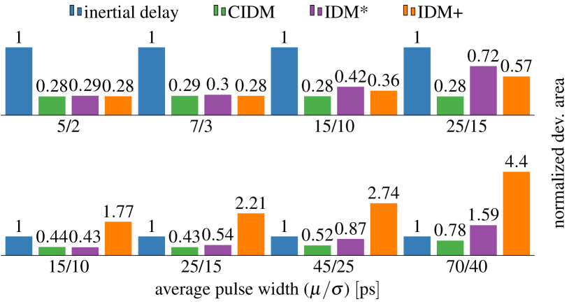
Since the signals are very steep near , the introduced error is typically rather small. This is even more pronounced due to the fact that the deviation of the input thresholds is usually smaller than that of the output thresholds due to the natural amplification of a gate. Note that this was verified by our simulations of the standard inverter chain. However, although the misprediction is small, it is introduced for each transition at every gate. While this might be negligible for small circuits like our chain, the error quickly accumulates for larger devices leading to deviations even for very broad pulses. Thus, the IDM* can be expected to deliver worse results than pure/inertial delay while being a computationally much more expensive approach. Indeed, for the gates used in our standard inverter chain, we recognized a clear bias towards for . Results for these delay functions are shown in Fig. 8. Finally, characterizing gates for CIDM was simply executed for .
The results for stimulating the standard inverter chain, with 2,500 normally distributed pulses of average duration and standard deviation , obtained by the Involution Tool for IDM*, IDM+, CIDM and the default inertial delay model, are shown in Fig. 8 (top). The accuracy of the model predictions are presented relative to our digitized SPICE simulations, which gets subtracted from the trace obtained with a digital delay model. Summing up the area (without considering the sign), we obtain a metric that can be used to compare the similarity of two traces. Since the absolute values of the area are inexpressive, we normalize the results and use the inertial delay model as baseline.
For short pulses, IDM*, IDM+ and CIDM perform similarly. We conjecture that this is a consequence of the narrow range for and (), and therefore the induced error due to non-perfect matchings in IDM+ is negligible. For broader pulses, we observe a reduced accuracy of IDM* and IDM+, which is primarily an artifact of the imperfect approximation of the real delay function by the ones supported by the Involution Tool. We even observed settings, where CIDM does not even beat the inertial delay model, which can also be traced to this cause.
For our custom inverter chain [Fig. 8 (bottom)], CIDM outperforms, as expected, the other models considerably, whereas IDM+ occasionally delivers poor results, even compared to inertial delays. This is a consequence of the non-matching threshold values and the accumulating error. IDM* achieves much better predictions, but still falls short compared to CIDM. For broader pulses, CIDM and the inertial delay model perform similar, since they use the same maximum delay and . The degradation of IDM* is once again a result of the imperfect delay function approximations.
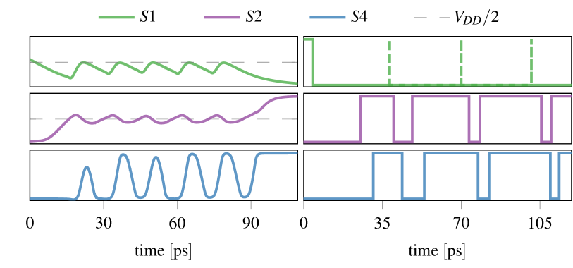
Finally, analog simulations in Fig. 9 revealed that an oscillation slightly below at the input of a low-threshold inverter can still result in full range switches at the end of the chain. For the fast IDM characterization such traces get removed. Note that albeit the presented oscillation is visible in IDM when characterized from back to front there are still infinitely many possibilities that can not be detected. Even if these do not propagate further it is important to know if the circuit has stabilized or not. The digital simulation results are shown in Fig. 9. While IDM removes the oscillation and thus does not indicate any transition at the output CIDM correctly predicts the regeneration of the pulses.
Note that we also added the capability to display the analog waveform that corresponds to the digital threshold crossings to the Involution Tool. This makes it possible for the user to investigate if the pulses are ill shaped and thus the circuit needs improvements.
To summarize the results of our experiments, we highlight that the characterization procedure for IDM either requires high effort (IDM*) or may lead to modeling inaccuracies (IDM+). The CIDM clearly outperforms all other models w.r.t. modeling accuracy for our custom inverter chain, and is also the only model that can faithfully predict the “de-cancellation” of sub-threshold pulses.
VIII Conclusions
We presented the Composable Involution Delay Model (CIDM), a generalization of the Involution Delay Model (IDM) that retains its faithful glitch-propagation properties. Its distinguishing properties are wider applicability, composability, easier characterization of the delay functions, and exposure of canceled pulse trains at interconnecting wires. The CIDM and our novel digital timing simulation algorithm have been developed on sound theoretical foundations, which allowed us to rigorously prove their properties. Analog and digital simulations for inverter chains were used to confirm our theoretical predictions. Despite this considerable step forward towards a faithful delay model, there is still some room for improvement, in particular, for accurately modeling the delay of multi-input gates.
References
- [1] S. H. Unger, “Asynchronous sequential switching circuits with unrestricted input changes,” IEEE Transaction on Computers, vol. 20, no. 12, pp. 1437–1444, 1971.
- [2] CCS Timing Library Characterization Guidelines, Synopsis Inc., October 2016, version 3.4.
- [3] Effective Current Source Model (ECSM) Timing and Power Specification, Cadence Design Systems, January 2015, version 2.1.2.
- [4] M. J. Bellido-Díaz, J. Juan-Chico, and M. Valencia, Logic-Timing Simulation and the Degradation Delay Model. London: Imperial College Press, 2006.
- [5] M. Függer, T. Nowak, and U. Schmid, “Unfaithful glitch propagation in existing binary circuit models,” IEEE Transactions on Computers, vol. 65, no. 3, pp. 964–978, March 2016.
- [6] M. Függer, R. Najvirt, T. Nowak, and U. Schmid, “Towards binary circuit models that faithfully capture physical solvability,” in Proceedings of the 2015 Design, Automation & Test in Europe Conference & Exhibition, ser. DATE ’15, San Jose, CA, USA, 2015, pp. 1455–1460.
- [7] M. Függer, R. Najvirt, T. Nowak, and U. Schmid, “A faithful binary circuit model,” IEEE Transactions on Computer-Aided Design of Integrated Circuits and Systems, vol. 39, no. 10, pp. 2784–2797, 2020.
- [8] D. Öhlinger, J. Maier, M. Függer, and U. Schmid, “The involution tool for accurate digital timing and power analysis,” Integration, vol. 76, pp. 87 – 98, 2021.
- [9] A. Asenov, “Random dopant induced threshold voltage lowering and fluctuations in sub-0.1 mu mosfet’s: A 3-d ”atomistic” simulation study,” IEEE Transactions on Electron Devices, vol. 45, no. 12, pp. 2505–2513, 1998.
- [10] T. Nikoubin et al., “Simple exact algorithm for transistor sizing of low-power high-speed arithmetic circuits,” VLSI Design, vol. 2010, Jan. 2010. [Online]. Available: https://doi.org/10.1155/2010/264390
- [11] W. Ibrahim and V. Beiu, “Reliability of nand-2 cmos gates from threshold voltage variations,” in 2009 International Conference on Innovations in Information Technology (IIT), 2009, pp. 135–139.
- [12] H. Gupta and B. Ghosh, “Transistor size optimization in digital circuits using ant colony optimization for continuous domain,” International Journal of Circuit Theory and Applications, vol. 42, no. 6, pp. 642–658, 2014.
- [13] J. Segura, J. L. Rossello, J. Morra, and H. Sigg, “A variable threshold voltage inverter for cmos programmable logic circuits,” IEEE Journal of Solid-State Circuits, vol. 33, no. 8, pp. 1262–1265, 1998.
- [14] J. Maier, “Modeling the cmos inverter using hybrid systems,” E182 - Institut für Technische Informatik; Technische Universität Wien, Tech. Rep. TUW-259633, 2017.
- [15] M. Martins et al., “Open cell library in 15nm freepdk technology,” in Proceedings of the 2015 Symposium on International Symposium on Physical Design, ser. ISPD ’15. New York, NY, USA: ACM, 2015, pp. 171–178.