Ultrafast Dynamics of the Surface Photovoltage in Potassium Doped Black Phosphorus
Abstract
Black phosphorus is a quasi-two-dimensional layered semiconductor with a narrow direct band gap of 0.3 eV. A giant surface Stark effect can be produced by the potassium doping of black phosphorus, leading to a semiconductor to semimetal phase transition originating from the creation of a strong surface dipole and associated band bending. By using time- and angle-resolved photoemission spectroscopy, we report the partial photoinduced screening of this band bending by the creation of a compensating surface photovoltage. We further resolve the detailed dynamics of this effect at the pertinent timescales and the related evolution of the band structure near the Fermi level. We demonstrate that after a fast rise time, the surface photovoltage exhibits a plateau over a few tens of picoseconds before decaying on the nanosecond timescale. We support our experimental results with simulations based on drift-diffusion equations.
I. INTRODUCTION
Semiconducting materials are the building block of modern technologies such as electronics, optoelectronics or computing devices. Their band gap is a fundamental property governing their optical and electrical abilities, leading in recent decades to an increasing amount of research aiming to enhance the control of both its size and its nature (direct or indirect). In this context, quasi two-dimensional (2D) materials have appeared as a new promising emergent familyChaves et al. (2020). Indeed, 2D semiconducting materials form a rich class of compounds whose electronic band gap can vary from 0 to more than 7 eV i.e. ranging from the terahertz to the infrared in monolayer XenesAk and Novoselov (2007); Vogt et al. (2012); Li et al. (2014a); Ji et al. (2016); Zhu et al. (2017); Kochat et al. (2018); Deng et al. (2018); Wu et al. (2019); Bihlmayer et al. (2020), to the visible with transition metal dichalcogenides (TMDCs)Manzeli et al. (2017) and finally to the ultraviolet with hexagonal boron nitrideElias et al. (2019) and 2D oxides Zhang et al. (2021); Lichtenstein et al. (2012); Kremer et al. (2019, 2021). In addition to covering a large part of the electromagnetic spectrum, the main advantage of quasi 2D materials is the possibility to tune their band gap with numerous approaches such as strainGuo et al. (2014); Rodin et al. (2014), electric fieldsRamasubramaniam et al. (2011), surface gatingKang et al. (2017), chemical substitutionGong et al. (2014); Ma et al. (2014), dimensionality reductionVillaos et al. (2019); Lin et al. (2020), or by the creation of complex heterostructuresNovoselov et al. (2016). Besides the band gap tunability, this opens a broad range of possibilities to create and engineer new quantum materials with unprecedented physical properties.
Among all these materials, black phosphorus (BP) is one of the most prominent because of its high carrier mobilitiesMorita (1986); Li et al. (2014b) and its tunable band gap over the whole infrared range, giving it a singular place between graphene and the TMDCsLing et al. (2015). BP is a layered semiconductor composed of only phosphorus atomic planes which are weakly interacting via out-of-plane van der Waals forces. Its band gap is highly dependent on the thickness, ranging from 0.3 eV in the bulk (BP) to 1.5 eV in the monolayer case (phosphorene). In addition to this intrinsic variety, external stimuli such as mechanical strain or surface chemical gating have been demonstrated as powerful tools to modify its electronic propertiesMu et al. (2019).
Chemical gating has attracted a lot of attention since the BP surface is very sensitive to external electric fieldsDolui and Quek (2015); Liu et al. (2017) and induced surface dipolesKim et al. (2015, 2017). Indeed, by doping the surface of BP with alkali atoms, it is possible to create a strong dipole generating an electric field responsible for the continuous reduction of the band gap at the surface. At a sufficient alkali coverage the band gap closes, as recently demonstrated by angle resolved photoemission spectroscopy (ARPES), creating a remarkable semiconductor to semimetal transitionKim et al. (2015). The electric field of alkali doped BP is related to the large electron transfer from the alkali atoms to the BP. It creates an excess of free carriers, leading to the formation of a space charge region (SCR) and band bending (BB), a generic effect in semiconductors physicsZhang and Yates Jr (2012). There is also a charges redistribution between the valence band (VB) and the conduction band (CB) whose wave functions are respectively pushed to the bulk and confined at the surface of the materialDolui and Quek (2015); Kim et al. (2015); Liu et al. (2017); Kim et al. (2017). In particular, the CB forms a two-dimensional electrons gas (2DEG)Kim et al. (2015); Kiraly et al. (2019) and experiences a larger BB, which can be decomposed in the same BB feeled by the VB () and a second one we name Stark potential (), localized at the extreme surface. At a sufficient coverage, the total CB bending is enough to close the surface band gap but the bulk one remains the same. In analogy with the atomic Stark effect created by an electric field, this is called the surface giant Stark effect.
In recent worksChen et al. (2020); Hedayat et al. (2021), it has been shown that in alkali doped BP at this critical coverage equals a few hundreds of meV and can be compensated via the illumination of the surface. Under the preexisting electric field, photo-generated electrons-holes are redistributed in the SCR and create a compensating field called surface photovoltage (SPV). Hedayat et al. reported that this is felt as an energy shift of the whole surface photoemission spectrum but also as a spectral shape modification of the VB Hedayat et al. (2021). However, their work mainly focussed on the transient dynamics up to 5 ps after the photoexcitation.
Here, we report on the temporal evolution of the SPV and the band structure near the Fermi level (EF) of potassium (K) doped BP, from a few ps before to a few hundreds ps after photoexcitation. To do so, we use time-resolved ARPES (Tr-ARPES) which is the ideal tool to study the ultrafast dynamics of the electronic structure of materials Bovensiepen and Kirchmann (2012); Smallwood et al. (2016). Tr-ARPES is particularly well suited since it allows the generation and the study of the SPV Widdra et al. (2003); Tokudomi et al. (2008); Tanaka (2012); Yang et al. (2014) with energy and time resolutions. Whereas it appears quasi instantaneously, the SPV is remarkably stable over 60 ps and decreases on the nanosecond (ns) timescale. We demonstrate that the characteristic timescales of the SPV are correlated to the spectral shape modification of the VB, which is highly affected by the potential profile in the SCR and as a consequence by the transient screening of . Furthermore, we solve the drift-diffusion equations (DDEs) for K doped BP and compare the simulated temporal evolution of the BB to the measured SPV dynamics. Our simulations show a good qualitative agreement and unambigously confirm the ultrafast transient evolution of after the photoexcitation of the pump. Finally, the calculations demonstrate the importance of the electron-hole recombination processes for the long-time evolution.
II. METHODS
Large single-crystals of BP were synthesized by a modified chemical vapor transport technique similar to the method first reported in Ref. Lange et al., 2007. Dry red phosphorus (150 mg, purity 99.999 ), dry SnI4 (5 mg, purity 99.999 ), tin shots (40 mg, purity 99.98 -purity), and gold powder (20 mg, purity 99.999 ) were sealed in an evacuated quartz glass tube. The mixture was placed in a box furnace at 680∘C and held at this temperature for 24 h. It was then cooled with 0.1 K/h to 500∘C and quenched to room temperature (RT) by removal from the furnace. The crystals were manually removed from the metals. Residual SnI4 was removed from the crystals by sealing them in an evacuated quartz tube and heating them to 400∘C for 5 h in a tube furnace. BP samples were cleaved at RT in a pressure of 1 10-8 mbar. ARPES measurements were performed using a ScientaOmicron DA30 photoelectron analyser with energy and angular resolutions better than 10 meV and 0.1°, respectively. The base pressure in the photoemission chamber was better than 3 10-11 mbar. For the static measurements, we used monochromatized HeIα radiation ( = 21.2 eV, SPECS UVLS with TMM 304 monochromator). For the Tr-ARPES measurements, half of the power of a femtosecond laser (Pharos, Light Conversion, operating at 1030 nm) is converted into 780 nm light with an optical parametric amplifier, which is then frequency-quadrupled to 6.3 eV in -BaB2O4 crystals to generate probe pulsesFaure et al. (2012). The pump-probe measurements were performed at 200 kHz and the pump fluence was 160 J/cm2. The intrinsic resolution of the probe laser is 47 meV, as determined by the fit of the Fermi edge of a polycrystalline metal. The remaining half of the fundamental laser power is directed into a collinear optical parametric amplifier (Orpheus, Light Conversion) to generate pump pulses at 780 nm (1.55 eV) with a duration of about 50 fs. The temporal resolution was estimated to be better than 100 fs by measuring the width of the cross-correlation between the pump and the probe pulses. We used and polarization for the probe and an incident angle of with respect to the normal of the surface to measure along the armchair (AC) and zigzag (ZZ) directions, respectively. The Tr-ARPES data have been acquired with a negative bias of -5 V. All the photoemission measurements were realized at 30 K if not further specified. The K evaporation was performed at 30 K from a SAES getter source in a pressure better than 2 10-10 mbar.
Density functional theory (DFT) calculations were performed using the projector augmented wave (PAW) method implemented in the Vienna ab-initio software package (VASP Kresse and Hafner (1993, 1994); Kresse and Furthmüller (1996a, b); Blöchl (1994); Kresse and Joubert (1999)), with kinetic energy cutoff 400 eV and k-point spacing 0.2 Å-1. Exchange and correlation effects were included within the strongly constrained and appropriately normed (SCAN Sun et al. (2015)) meta-generalized gradient approximation. The structure of BP was relaxed until the residual forces on atoms were smaller than 1 meV/Å. The lattice parameters obtained after the relaxation of the structure with DFT calculations in the SCAN approximation are a = 4.53 Å , b = 3.29 Å and c = 10.91 Å , in good agreement with x-ray diffraction measurements Brown and Rundqvist (1965).
III. RESULTS
A. Static Characterization of Black Phosphorus

The crystal structure of BP is shown in Fig. 1(a). It crystallises in an orthorhombic crystal structure (space group Cmca) with superimposed buckled layers of phosphorus atoms along the axis. The layered structure of BP and the weak interlayer van der Waals interactions favor mechanical cleaving of the material with the scotch-tape technique. The strongly anisotropic nature of BP in the basal plane is visible in its two high-symmetry directions along and , namely the AC and ZZ directions. The corresponding three dimensional Brillouin zone (BZ) and its 2D projection on the (001) plane (green), i.e. the cleave plane, are shown in Fig. 1(b).
The static electronic band structure of pristine BP along the AC direction measured by ARPES is shown in Fig. 1(c) (note that the signal has been symmetrised with respect to the point). At this particular photon energy, we almost probe the in-plane high-symmetry line of the BZTakahashi et al. (1986) (thick red line in Fig. 1(b)). The ARPES intensity exhibits all the spectroscopic signatures of a clean BP surfaceGolias et al. (2016). In these energy and momentum ranges, the band structure is composed of six dispersive bands with the VB top presenting a maximum at the point and located about 0.1 eV below EF. In Fig. 1(d), we compare our experimental data with bulk projected DFT calculations i.e. the superposition of the calculated band structure of BP along the direction, from the to the point of the 3D BZ (red plane in Fig. 1(b)). The overall agreement between ARPES and DFT is excellent. Furthermore, the intensity variations and the energy broadening of the bands are also well reproduced.
B. Dynamics of the Surface Photovoltage in K Doped Black Phosphorus
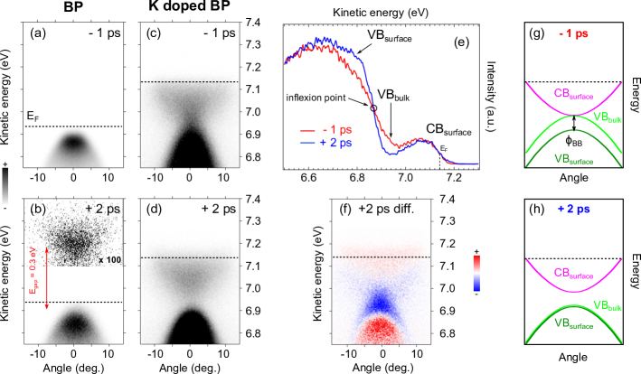
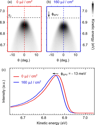
Since the static ARPES only gives access to the occupied part of the band structure, we now turn our attention to Tr-ARPES measurements in order to obtain the band gap of BP. Figure 2(a,b) show the corresponding data taken at a pump-probe delay of -1 ps and +2 ps along the ZZ direction, respectively. We are using this orientation in the following because of detrimental matrix element effects along the AC direction. At negative delays, we only see the occupied part of the band structure as in the static case (shifted by the SPV as discussed below). At positive delay, the CB is now transiently populated and can be probed. Thus, we can directly estimate the band gap amplitude of the material to be 0.3 eV, in good agreement with previous measurements Kiraly et al. (2017); Qiu et al. (2017) and our DFT calculations from Fig. 1(d) which give a band gap value of 307 meV.
As visible in Fig. 2(b), EF is closer to the VB than to the CB. Since the effective masses of these bands are almost the same in pure BPMorita (1986), it means that our sample is p-doped. Recent scanning tunneling microscopy (STM) experiments have demonstrated that p-doped BP samples have an important density of surface acceptor statesQiu et al. (2017). This is confirmed by our measurements showing that photoexcitation of the pump induces a global shift of -13 meV of the photoemission spectrum (see Fig. 7), i.e. a shift to low kinetic energy (KE), originating from a negative SPV as expected by the existence of an upward BB at the surface of our sampleZhang and Yates Jr (2012). This negative SPV compensates the initial upward BB at the surface of our p-doped BP sample. We illustrate the situation in Fig. 3(a), where we plot the energy band diagrams of the p-doped BP surface. We consider the nonequilibrium, the equilibrium and finally the photoexcited configurations.
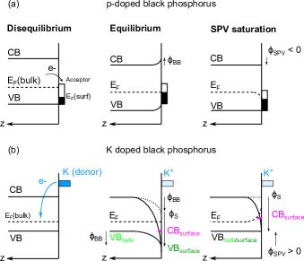
At a negative pump-probe delay, the photoelectrons travelling from the surface to the photoemission analyser are decelerated/accelerated (depending on the initial BB curvature) by the electric field generated by the SPV due to the pump pulse arriving afterwardsTanaka (2012); Yang et al. (2014). The experimental consequence is a rigid KE shift of the entire photoemission spectrum. In other words, at negative delays we probe the spatial distribution of the electric field generated outside the sample by the SPV, but not the photoexcited band structure of the material. At positive delays, we are sensitive to the modification of the band structure induced by the SPV.
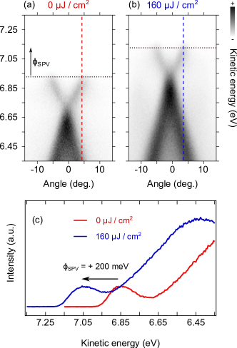
Subsequently, we have deposited K atoms on the BP surface until reaching the semiconductor to semimetal transition, as depicted in Fig. 2(c). This panel shows the Tr-ARPES intensity taken at -1 ps pump-probe delay. Compared to the pristine BP surface, the VB has shifted down by 200 meV relative to EF whereas the CB is now visible in the occupied states and touches the top of the VB. By doping the surface with electrons from donor atoms, we switch from an upward to a strongly downward BB configuration. This is the reason why we now observe a positive SPV at the origin of a global shift to high KE of the whole photoemission spectrum (see Fig. 8 for measurements with and without pump). Both VB and CB feel this common BB, namely , but the CB also experiences a Stark potential at the extreme surface and forms a 2DEG. As a consequence, its total bending is larger than the VB one and, at a suffisient K coverage, lead to a collapse of the surface band gap. At the low fluence used in our experiment, we do not screen this strong Stark potential which is confined in the first layers of BP and, consequently, the 2DEG of the CB persists. The coexistence of a long range BB and a strong surface potential appears to be a common effect in layered semiconducting materials Papalazarou et al. (2018). Similarly to the VB, the 2DEG is only energy shifted by the SPV and the associated screening of (see Fig. 3(b)).
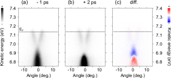
Let us now discuss the measurement taken at +2 ps and presented in Fig. 2(d). The most striking effect relates to the top of the VB which is shifted to low KE: the gap between the CB and the VB is apparently reopened. This is even more evident by looking at the energy-distribution curves (EDCs) taken at -1 ps and +2 ps (see Fig. 2(e)) or the difference in ARPES intensity between these two pump-probe delays (see Fig. 2(f)). It is worth to mention that this effect is independent of the crystal orientation, as shown in Fig. 9. Nevertheless, it is more convenient to work along the ZZ line because the CB has no spectral weight at the normal emission along the AC direction due to matrix element effects Chen et al. (2018).
The EDCs in Fig. 2(e) clearly show that the spectral shape of the VB is unambiguously affected by the photoexcitation at positive pump-probe delay. Indeed, the leading edge of the VB is strongly sharpened, leading to a depletion of intensity at 6.95 eV and an increase of intensity at 6.8 eV KE, visible as a blue/white/red contrast in the difference ARPES intensity plot in Fig. 2(f). In contrast, the CB spectral shape is marginally affected. By consequence, we confirm that the effect of the SPV on the VB is not limited to a global energy shift of the band structure; it also modifies its spectral shapeHedayat et al. (2021).
At negative delay, we probe the equilibrium state of the system for which the common BB, , is not yet screened. Since the VB is delocalised in the bulk of the material and the 6.3 eV laser is bulk sensitive (several nm) due to the extraction of very low kinetic energy electrons Seah and Dench (1979), we integrate both the contributions of the VB from the surface and the bulk which are energy separated by the amplitude of , i.e. almost 200 meV (see Fig. 3(b)). The corresponding sketch of the band structure is represented in Fig. 2(g). It explains why the VB width is larger at negative delay, as observed in Fig. 2(e). On the contrary, the CB forms a 2DEG confined at the surface and is visible as a single band we call CBsurface, which aligns with the bulk contribution of the VB.
At positive delay, we now probe the photoexcited system at a pump fluence of 160 J/cm2. At this fluence, the SPV is saturated Chen et al. (2020) and we recover a flat band regime for the VB: surface and bulk contributions of the VB are now aligned (see Fig. 3(b)). In contrast, the 2DEG persists because the Stark potential is not screened at this fluence. The consequence is that the bulk contribution of the VB shifts relatively to the surface one and to EF, leading to a decrease of the VB width and to a sharpening of its leading edge, as visible in Fig. 2(e). This is also the reason why CBsurface and the bulk contribution of the VB are now energy separated and why we observe an apparent transient band gap reopening. This second situation is schematized in Fig. 2(h). It is apparent because, in reality, the surface band gap was not closed since CBsurface and VBsurface are energy separated by 200 meV, as revealed once is compensated by the SPV (Fig. 2(d)). With our K coverage, the surface band gap has not yet collapsed and has only been reduced by 100 meV with respect to the bulk band gap of BP.
Nevertheless, it is an additionnal evidence that the surface band gap can be reduced with respect to the bulk by alkali doping. By supressing the photoemission artefact related to the integration of the VB along the out-of-place direction, we access the true surface band gap amplitude. For this reason, the claim of a semiconductor to semimetal transition has to be used carefully since it is only true (i) in the first layers of BP where the Stark potential exists and (ii) it is dependent on the depth integration of the technique, which varies with the photon energy in ARPES.
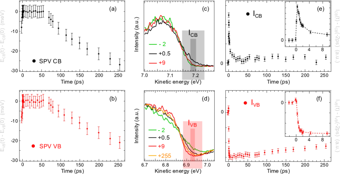
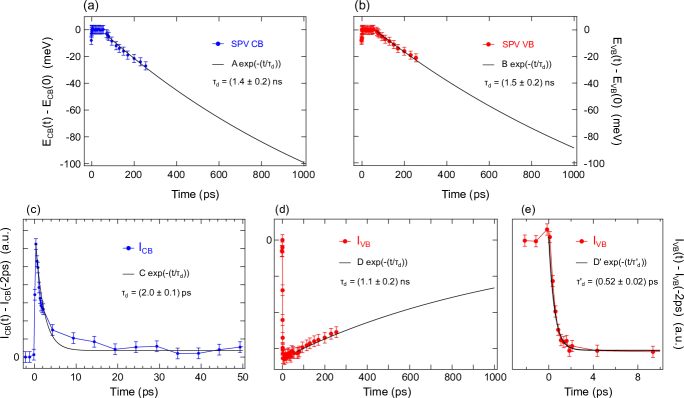
Thus, in this scenario the spectral shape evolution of the VB is directly correlated to the photoinduced SPV at positive delay. To confirm this, it is important to show that the SPV dynamics is unambiguously related to the dynamics of the spectral shape of the VB. First, we characterized the energy shift induced by the SPV both at negative and positive delays over a few hundreds of ps. To do so, we estimated the energy shift of the photoemission spectra as extracted from the EDCs analysis as a function of time (see a few EDCs at different pump-probe delays in Fig. 10(a)). The energy shift has been evaluated as the evolution of the position of the leading edge inflexion point of both the VB and the CB. The corresponding results are presented in Fig. 4(a,b). It is important to mention that the energy position of the inflexion point is independent of the evolution of the spectral shape and consequently only reflects the evolution of the experimentally measured SPV (in other words the position of CBsurface and VBsurface).
In both cases, the SPV is increasing at negative delays up to a maximum around time zero. Then, it exhibits a remarkable plateau over 60 ps before slowly decaying over a few hundreds of ps. We have fitted the recovery of the SPV with an exponential fit. The extracted time constants for the CB and the VB are 1 ns (see Fig. 11(a,b)). The temporal evolution of the photoemission cutoff position shows the same features (see Fig. 10(b)). Thus, the energy shift induced by the SPV is the same for all the photoemission spectrum and not restricted to a particular KE range.
Now, we address the temporal evolution of the spectral shape of the bands. In order to remove the influence of the energy shift induced by the SPV, we have plotted the EDCs corrected by the above determined SPV for both the CB and the VB, as shown in Fig. 4(c,d) for selected pump-probe delays. To understand the temporal evolution of the spectral shape, we have plotted the variation of the photoemission intensity above the energy position of the inflexion points for both the CB and the VB (it would be the complementary of taking an integration region below these points). The integration regions are highlighted by the grey and red rectangles. These plots are represented in Fig. 4(e,f) and respectively called ICB and IVB.
The temporal evolution of ICB shows a strong increase around time zero before decaying over a few ps to its equilibrium value (see inset in panel (e)). It can be reproduced by an exponential fit with a time constant of 2 ps (see Fig. 11(c)) which is expected for the transient dynamics of the electronic temperature Sobota et al. (2012). Thus, the effect of the SPV on the CB is limited to an energy shift and its spectral shape is not modified as expected by the strong surface confinement of electrons from the CB in the above mentioned scenario.
On the contrary, the evolution of IVB is more complex. Over the first ps after photoexcitation, IVB is drastically reduced: it corresponds to the intensity depletion we discussed in Fig. 2. This decrease can be reproduced by an exponential fit with a time constant of 520 fs (see Fig. 11(e)). During the next 60 ps, IVB shows a plateau before slowly recovering with a time constant of 1.1 ns (see Fig. 11(d)). The plateau and the recovery timescales of IVB are in very good agreement with the ones observed for the SPV. Thus, it unambiguously demonstrates that the spectral shape evolution of the VB in K doped BP is directly related to the magnitude of the SPV in the material. We can further note that, as expected and contrary to the experimentally measured SPV, IVB is not affected at negative delays because we probe the band structure of the unexcited system, i.e. before the pump pulse arrival.
C. Discussion and Simulations
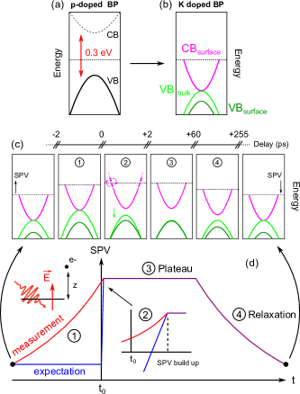
We now summarize the above discussed evolution of the band structure, both in the static and dynamic cases. By doping the surface of a p-doped BP sample with K, we create a strong surface dipole which is the origin of the surface confinement and the shift of the CB down to the occupied states. At a sufficient coverage, the CBsurface and the bulk contribution of the buried VB superimpose, visible as a band gap closing in static ARPES (Fig. 5(a,b)). By photoexciting the system with an intense infrared laser pulse, we induce and reveal the dynamics of the SPV, which is responsible for the shift of the whole surface photoemission spectrum and for the transient modification of the VB spectral shape.
The pertinent timescales are given in Fig. 5(c) and can be decomposed into four main steps. (i) At negative delays, since the probe induces photoemission before the pump arrival, we are sensitive to the non-photoexcited band structure of the system. Nevertheless, the photoemission spectrum is shifted to higher KE by the electric field generated afterwards by the pump pulse. The smaller the pump-probe delay, the larger the field experienced by the outgoing photoelectrons. At a sufficient time before the pump excitation, the photoelectrons are not sensitive to this electric field anymore and the band structure looks the same as in the static case (see the extreme left panel). (ii) During the first picoseconds after photoexcitation, i.e. at positive delays, two processes are occuring. Firstly, a SPV quickly builds up and modifies the energy level diagram of the system. The VB is largely affected because it is delocalized in the bulk of BP while the surface confined CBsurface is not altered. The consequence is the transient modification of the VB spectral shape and the apparent reopening of the band gap. Secondly, the pump pulse drives the system to a highly excited state. The electronic temperature increases, progressively equilibrates with the lattice and decreases: the consequence is a transient broadening of the Fermi-Dirac distribution in the first ps after the photoexcitation. (iii) Once the electronic temperature equilibrates and the band gap apparently reopens, the system exhibits a remarkable quasi steady state over 60 ps. (iv) Then, the SPV progressively recovers with a time constant of the order of ns. The consequence is a progressive shift to lower KE this time and a recovery of the VB spectral shape. At a sufficient time after the pump excitation, the SPV has fully recovered and the band structure is similar to the one observed a long time before the photoexcitation or in the static case (see the extreme right panel).
In Fig. 5(d), we give a schematic representation of the SPV time evolution as experimentally measured with Tr-ARPES (red curve), and as we would expect from theory (blue curve). Before time zero, the progressive increase of the experimentally extracted SPV is an artefact of the pump-probe approach, as discussed above. As schematized in the step 1, we are theoretically expecting a zero SPV in this time regime (see blue curve). At time zero, the system is photoexcited and the SPV builds up (step 2). As discussed below, it occurs on the timescale of the pump pulse ( 50 fs). In theory, the SPV starts from zero before building up to its maximum after this characteristic time (without step 1). This is in contrast with the experimentally measured SPV which is already at an almost maximum value around time zero due to the step 1, further complicating its experimental resolution. Steps 3 and 4 are similar in both cases with a plateau and relaxation processes.
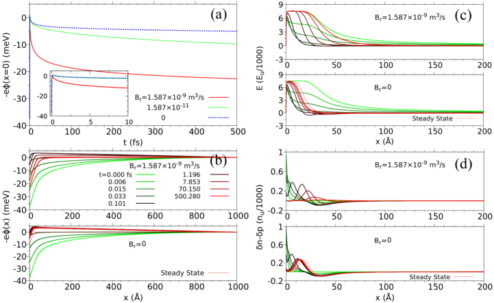
In order to simulate the non-equilibrium dynamics of photo-excited carriers in K doped BP at K we solve the DDEs with realistic parameters (see appendix). Since we are looking at the effect of the photoexcitation of the pump on the common long-range BB, i.e. , we assume that the depth profile potential of the CB and the VB are the same. The results are shown in Fig. 6. While electron-hole recombination can be neglected on the sub-ps timescales of the simulation, we also show results with an artificially short life time of the photocarriers. In these simulations, the band-to-band recombination Li (2016) between excess electron-hole pairs results from a term ( with the static free electron distribution) in the DDEs, where is the recombination rate and () is the excess density of electrons (holes) generated by the laser pump. The SPV amplitude is plotted as a function of time in Fig. 6(a). An ultrafast increase of is observed for fs, as a result of two main factors. On the one hand, there is a large discrepancy between the high mobility of the holes, , and the smaller mobility of electrons at KMorita (1986). On the other hand, a strong internal electric field ( ) exists in the surface region due to the spatial separation between the K ions and the free electrons (see Fig. 12). The drift velocity of the holes and electrons can reach Å and Å, respectively 111We caution here that the sub-fs timescale is obtained by assuming that the experimental mobilities are still valid for such a very high electric field. In practice, this might not be the case, resulting potentially a longer rise-time. As long as it remains shorter than the pump duration, our conclusions are not qualitatively affected.. As a result, the holes flow rapidly into the bulk (the direction of the net field), while the electrons flow towards the surface. The time evolution of the excess carrier density, , plotted in Fig. 6(d), illustrates how excess electrons rapidly accumulate near the surface while an excess of holes rapidly builds up slightly away from the surface. The effect of this reshuffling of charge is a rapid weakening of the internal electric field, as shown in Fig. 6(c), and a rapid flattening of the energy band , i.e. , as shown in Fig. 6(b).
The diffusion term becomes important when the density profile is sharp. It causes particles to flow from the high density region to the lower density region. As we can see from Fig. 6(d), the surface peak of decreases with time and a broader peak appears which moves toward the bulk. At fs, the internal electric field stops weakening and reaches its maximum value as shown in Fig. 6(a). For fs, the surface peak in the net charge density begins to disappear slowly and shifts further into the bulk region. As a result, the internal electric field starts to increase again and some BB reappears, as shown in Fig. 6(b). We should note that these simulations are for an instantaneous photo-doping at . In our experiment, the pump pulse has a duration of about 50 fs. Hence, in the experiment, the flattening of the band should occur on a timescale controlled by the pump pulse.
Without recombination between electrons and holes (), the system will relax to a new steady state controlled by the different electron and hole mobilities. As shown by the lower panel of Fig. 6(d), the time-evolution of approaches this steady state solution (red dashed line) rather slowly after fs. This solution corresponds to an almost flat band, which is distinctly different from the initial equilibrium solution (green line in Fig. 6(b)). Hence, as shown by the blue-dashed line in Fig. 6(a), will eventually reach a plateau much higher than its initial value at .
If we switch on recombination processes () (with a rate much larger than in the realistic system), the peak starts to decay even on the timescale of our simulation, see the upper panel in Fig. 6(d). Now, the system will return to the initial equilibrium state and we observe a continuous recovery of the BB, as shown by the green and red lines in Fig. 6(a) and also in the upper panel of Fig. 6(b). The higher the recombination rate, the faster the return to the initial state.
These simulations present a good qualitative agreement with our Tr-ARPES measurements. Very quickly after the system is excited by the pump pulse, the photogenerated charge carriers are redistributed in the SCR under the effect of the pre-existing electric field and diffusion. This charge redistribution leads to a transient compensation of the electric field at the surface, and as a consequence to a compensation of the initial BB. As experimentally extracted from the transient evolution of the VB (see Fig. 4(f)), the SPV builds up in the first ps. According to our quench calculations, it happens on the fs timescale (see Fig. 6(b)). There are two reasons for this discrepancy. Firstly, in the experiment the photoexcitation occurs with a finite duration of about 50 fs and the total time resolution of our experiment is 100 fs, well above this timescale. Secondly, it has been demonstrated in the pristine BP case that a fast transient broadening of the VB happens in the first ps after the photoexcitation Chen et al. (2018). This effect is still present in the K doped caseHedayat et al. (2021) and explain the very fast increase of intensity in Fig. 4(f), which is quickly vanishing and counterbalanced by the depletion caused by the SPV. Consequently, limited pulses duration and transient broadening explain why the time trace in Fig. 4(f) is broadened and why the measured time constant of the SPV build up has a finite duration 500 fs.
Then, the delayed recombination (the plateau on Fig. 5(d)) regime is experimentally seen, but not captured by our theoretical model. Such features have already been observed in other systems such as silicon oxideWiddra et al. (2003) or GaAsTokudomi et al. (2008) but, to the best of our knowledge, no model has been able to explain it. We speculate that the origin of this delayed recombination could be due to an additional effect, not captured by our theoretical model, that prevents the recombination of electrons and holes immediately after the pump, like spatial separation or the trapping by defects. Another possibility is that, in this temporal regime, recombination takes place but is exactly compensated by another effect which is unknown to us. We leave the explanation of the origin of this feature for future works.
Finally, the calculations unambiguously demonstrate that the relaxation regime can only be explained by taking into account a recombination term of the photoexcited charge carriers, otherwise the system would remain in a photo-doped nonequilibrium state with almost zero BB indefinitely, which is not observed experimentally.
Overall, our dynamic simulations based on the solution of the DDEs equations satisfactorily capture the physics of the problem (as expected in Fig. 5(d)), although simulations with realistically slow recombination times were not possible. Since simulations up to ns timescales are beyond our capabilities we had to choose extremely fast recombination times (a few fs against ns). Still these calculations demonstrate that the relaxation of the band structure on a timescale is controlled by the electron-hole recombination.
IV. CONCLUSIONS
To summarize, the ultrafast dynamics of the SPV in photoexcited K doped BP has been measured with Tr-ARPES and compared to numerical simulations of the DDEs. We analysed the detailed temporal evolution of the SPV and the band structure near the Fermi level, from a few ps before to a few hundreds ps after the photoexcitation. Our results demonstrate that the timescales of the SPV and the spectral shape modication of the VB are correlated, and support the scenario where the transient screening of is responsible for the apparent reopening of the band gap. Our simulations confirm the ultrafast transient evolution of (on the timescale of the pump pulse) and the importance of the electron-hole recombination processes for the long-time evolution. Without recombination, the system would remain trapped in a nonequilibrium steady state with almost no BB.
Our experimental observations and our theoretical approach are very general and should have implications also for other Tr-ARPES measurements of 2D semiconducting materials with significant BB. In particular, care has to be taken in the interpretation of transient spectral shape modications, since these may reflect the evolution of the SPV rather than qualitative changes in the band structure.
ACKNOWLEDGMENTS
This project was supported by the Swiss National Science Foundation (SNSF) Grants No. P00P2170597, No. 200021-165539 and No. 200021-196966. The calculations have been performed on the Beo05 cluster at the University of Fribourg. We are very grateful to P. Aebi for sharing with us his photoemission setup. Skillful technical assistance was provided by J.L. Andrey, M. Andrey, F. Bourqui, B. Hediger and O. Raetzo.
APPENDIX
1. SPV Characterization in Pristine Black Phosphorus
Figure 7 displays the Tr-ARPES measurements of BP at -1 ps pump-probe delay without (red) and with (blue) the pump. From this, it is possible to evaluate the magnitude and the sign of the SPV. We observe that the blue spectrum is shifted by 13 meV to low KE with respect to the red one. Since the pristine BP surface is p doped due to the presence of surface acceptor states, an upward BB of the VB is expected as illustrated in the middle panel of Fig. 3(a). This is confirmed by the negative value of the SPV which is compensating the upward BB.
2. SPV Characterization in K Doped Black Phosphorus
As discussed above in the p-doped BP case, Fig. 8 displays the Tr-ARPES measurements of K doped BP at -1 ps pump-probe delay without (red) and with (blue) the pump. In contrast to the pristine BP case, we observe that the blue spectrum is shifted by 200 meV to high KE with respect to the red one. Due to the strong surface dipole, a long-range downward BB of both the CB and the VB is expected as illustrated in the middle panel of Fig. 3(b). This is confirmed by the large positive value of the SPV which is compensating this BB.
3. Evidence of Spectral Shape Modification Along the Armchair Direction
In Fig. 9, we show that the spectral shape modification of the VB is also visible along the AC direction. As discussed in the case of the ZZ direction in Fig. 2 of the main text, we observe the same blue/white/red contrast in the difference plot (see Fig 9(c)) before and after the photoexcitation of the pump. The main difference with the ZZ direction is the absence of spectral weight at the bottom of CB, as already discussed in Ref. Chen et al., 2018.
4. Raws EDCs and Photoemission Cutoff Dynamics
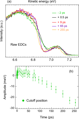
Figure 10(a) displays EDCs of the K doped BP sample taken at normal emission showing both a time dependent energy shift and VB spectral shape evolution. In contrast, the CB is only energy shifted. This is a selection of EDCs we used to produce Fig. 4(a,b). Figure 10(b) shows the temporal evolution of the low energy electrons cutoff position. Its shape is similar to the time dependent SPV of the VB and CB (see Fig. 4(a,b)).
5. Time Constants as Obtained by Exponential Fits
In Fig. 11, we give a systematic fit of the pertinent time constants discussed in the main text, for both the VB and the CB of photoexcited K doped BP.
6. Simulation of the Carrier Dynamics in Photoexcited Black Phosphorus
I Model and parameters
Pristine bulk BP is an intrinsically p-doped semiconductor with a small band gap of eV Morita (1986); Chen et al. (2018). The intrinsic carrier density can be as large as at K Bhaskar et al. (2016), but at very low temperature, (and also ) decays exponentially with decreasing . At the temperature of the experiment, , the density is as small as 0.016 and thus negligible. In order to electron dope the system, K atoms are deposited on the surface of BP. These K atoms release their electrons into the sample and create a 2D electron gas near the (positively charged) surface. The spatial separation between the ionized K atoms and the electron gas creates a strong electric field Kim et al. (2015). When electron-hole pairs are created by the pump, their dynamics is affected by this field and by the different mobilities in the VB and CB.
The BB along the axis is mainly controlled by the carrier dynamics along the direction. Assuming a homogeneous system in the - plane, we consider a one-dimensional drift-diffusion problem along the axis. The mobilities of the electrons and holes in BP are taken from Ref. Akahama et al., 1983. At K, and , which makes the drift velocity as large as Å. Thus the simulation needs a timestep of the order of attoseconds to resolve the ultrafast carrier dynamics.
In the simulation, we assume a sample thickness of Å, which is large compared to the atomic scales, but much smaller than the actual sample thickness (). There are two reasons for this choice. On the one hand, the strong electric field requires a real-space grid spacing as small as Å. Thus a realistic thickness requires huge matrices of dimension which is computationally very demanding. On the other hand, the penetration depth of the pump pulse is only , and as we will show, the net difference in the electron and hole population is significant only in a narrow region near the surface. Hence, the relevant short-time carrier dynamics takes place near the surface.
Furthermore, we assume that the photoexcited electron-hole pairs, with densities and , are generated instantaneously at time , with an exponential profile (see Fig. 12)
| (1) |
where the surface photoexcited carrier density and the penetration depth Å are chosen in accordance with the experiment. The total density (per area) of photoexcited electron-hole pairs is denoted by . The K atoms are assumed to be deposited near the surface with a distribution that decays exponentially into the bulk, , where is the unit of density and Å represents the doping depth, while is the total K coverage per unit area. In the case of a -function distribution of K ions, the thickness of the 2D electron gas is less than 1 Å, which is unrealistic. A more accurate quantum mechanical treatment based on a Schrödinger-Poisson solver would yield a broader charge distribution, and the above exponential profile for is a simple way of mimicking this effect.
As for the carrier densities and , we neglect the intrinsic densities Davies (1997)
| (2) |
where the averaged effective masses are and Morita (1986) and the band gap is eV. At temperature K, which is much smaller than the excess carrier density Bhaskar et al. (2016) (see also Fig. 3 of Ref. Bhaskar et al., 2016. Even at K, ). We only consider the photo-excited electron-hole densities (, ) and the free electron density () resulting from the fully ionized K atoms with surface density . Hence, the total electron and hole densities are
| (3) |
and
| (4) |
All the simulation parameters are listed in Tab. 1.
| Name | Symbol | Value |
|---|---|---|
| Temperature | 30K | |
| Relative Permittivity | 8.3 | |
| Electron Mobility | ||
| Electron Diffusion Coefficient | ||
| Hole Mobility | ||
| Hole Diffusion Coefficient | ||
| Potassium Coverage | ||
| Photoexcited Carrier Volume | ||
| Length Unit | ||
| Sample Length | L | |
| Number of -grid points | N | 20001 |
| Electric Field Unit | ||
| Density Unit | ||
| Radiative Recombination Rate |
II Numerical Simulation
II.1 Drift-Diffusion Equations
The continuity equations for the electrons and holes read
| (5) |
and
| (6) |
respectively. Here, the particle flux densities are
| (7) |
for the electrons and
| (8) |
for the holes. are the drift mobilities and the diffusion coefficients which are related to by the Einstein relations . and denote the generation rate and recombination rate, respectively. To illustrate the effect of recombination, we make the simple ad hoc approximation
| (9) |
Here we neglect the thermal generations and recombinations and consider only inter-band recombinations Li (2016).
Combining eqs. 3, 4, 5, 6, 7, 8 and 9, we arrive at the drift-diffusion equations
| (10) |
| (11) |
Furthermore, the total electric field and total charge density satisfy the Poisson equation
| (12) |
where with the relative permittivity and the vacuum permittivity.
For the stability of the simulation, it is advantageous to reformulate these equations in terms of and . The free electron distribution is obtained by solving the static (equilibrium) problem before the pump ( for )
| (13) |
| (14) |
The numerical method used for computing the static and is described in section II.2, where we have to set . Equation (10) can then be rewritten as
| (15) |
where and
| (16) |
For given and , we calculate and as
| (17) |
II.1.1 Discretization
The density and electric field are continuous functions of the coordinate and time . Numerically, we discretize and as and , and define . Let denote the value of the function at and , and , . The first- and second-order derivative with respect to of a given function can be represented in a matrix-vector multiplication form, and , where and denote the finite difference matrices for the first and second-order derivative, respectively. Here, we will use the central difference approximation to and ,
| (18) |
One needs to properly treat the zero-flux boundary conditions (eqs. 7 and 8) which are equivalent to
| (19) |
since due to charge neutrality. By introducing two auxiliary points and , we can write (using as an example)
| (20) |
which gives and . Thus
| (21) |
Hence, we can write the finite-difference matrices for the density as
| (22) |
and
| (23) |
II.1.2 Semi-implicit Euler Method
The coupled eqs. 15, 11, 12 and 16 are solved by using a semi-implicit Euler method:
| (24) |
and
| (25) |
Here, represents a diagonal matrix with the elements of the vector . and are calculated from eq. 17 using the density at and similarly for and .
Eqs. (24) and (25) can be reduced to the linear equations
| (26) |
and
| (27) |
The numerical simulation consists of the following steps:
-
1.
Find the static solution ( and ) before the pump (see section II.2); turn on the pump as in eq. 1 at ().
- 2.
- 3.
-
4.
Repeat steps 2 and 3 until .
For any intermediate time , we can calculate the potential profile as
| (28) |
where the potential reference is chosen as . The band bending profile is given by
| (29) |
and the surface photovoltage is given by .
II.2 Steady state solution
Without recombination term in eqs. 10 and 11, the photoexcited carriers drift and diffuse inside the material and eventually reach a steady state. In this steady state, the current is zero everywhere
| (30) |
| (31) |
To find the steady state solution, we need to solve the coupled eqs. 12, 30 and 31.
II.2.1 Dimensionless formulation
For simplicity, we split into three components, , with , and . Furthermore, we introduce the unit for the electric field and for the density, and introduce the unit-less functions , and for , and , respectively. can be easily calculated from the known as , with . We can thus simplify eqs. 30 and 31 as
| (32) |
and
| (33) |
Now we introduce the unit-less coefficient
| (34) |
which allows to simplify eqs. 32 and 33 as
| (35) |
and
| (36) |
We furthermore introduce the two auxiliary functions , which simplify the implementation of the boundary conditions, as shown below. The sum of Eq. (35) and Eq. (36) gives
| (37) |
while the difference of Eq. (35) and Eq. (36) gives
| (38) |
In the solution of the coupled second-order non-linear differential eqs. 37 and 38 on the discretized grid points , we need to impose the proper boundary conditions for and . In the following, we represent a function on the grid points by a vector with the -th element labeled as for simplicity. The conditions to be imposed are the following:
-
1.
Charge neutrality requires that the electric field vanishes at the boundaries, i.e., . Since , we thus have and if .
-
2.
The electric field component arising from , i.e. , satisfies . Furthermore, the Gauss law requires that . Thus we have , which gives and .
-
3.
, since is zero at the boundaries.
II.2.2 Newton-Raphson Iterative Method
Solving eqs. 37 and 38 for and is equivalent to solving a multivariable root problem . The Newton-Raphson iterative method Press et al. (2007) is based on the first order Taylor expansion of as , where denotes the Jacobian matrix with elements . By setting , we obtain a set of linear equations for :
| (39) |
is the correction to and we update the solution as
| (40) |
until convergence.
To utilize the Newton-Raphson method, we need to combine eqs. 37 and 38 into a matrix form. Since , , , and are constants given by the boundary conditions, we only need to define the finite-difference matrices on the internal grid points with
| (41) |
and
| (42) |
Let’s introduce the vectors
| (43) |
and
| (44) |
(, ). The first and second derivatives are given by
| (45) |
Now we define the vector from eqs. 37 and 38 as
| (50) | ||||
| (53) |
The Jacobian matrix reads
| (56) | ||||
| (59) |
According to eq. 40, and are updated as
| (60) |
after solving the linear equation
| (61) |
II.3 Static State
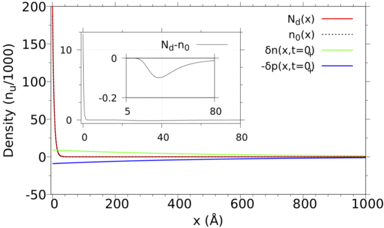
The static equilibrium state before the pump can be obtained in a similar manner as described in section II.2, by setting the parameter to zero. In Fig. 12, the distribution of is shown as the red line, and the distribution of free electrons from ionized K is shown as the black dashed line. The inset shows the difference between and near the surface region. The sharp surface peak and the small broad peak in at Å imply a spatial separation between the K ions and the free electrons, and this gives rise to a strong internal electric field in this region, as shown by the green line () in Fig. 6(c).
References
- Chaves et al. (2020) A. Chaves, J. Azadani, H. Alsalman, D. da Costa, R. Frisenda, A. Chaves, S. H. Song, Y. Kim, D. He, J. Zhou, et al., Npj 2D Mater. Appl. 4, 1 (2020).
- Ak and Novoselov (2007) G. Ak and K. Novoselov, Nat Mater 6, 183 (2007).
- Vogt et al. (2012) P. Vogt, P. De Padova, C. Quaresima, J. Avila, E. Frantzeskakis, M. C. Asensio, A. Resta, B. Ealet, and G. Le Lay, Phys. Rev. Lett. 108, 155501 (2012).
- Li et al. (2014a) L. Li, S.-z. Lu, J. Pan, Z. Qin, Y.-q. Wang, Y. Wang, G.-y. Cao, S. Du, and H.-J. Gao, Adv. Mater. 26, 4820 (2014a).
- Ji et al. (2016) J. Ji, X. Song, J. Liu, Z. Yan, C. Huo, S. Zhang, M. Su, L. Liao, W. Wang, Z. Ni, et al., Nat. Commun. 7, 1 (2016).
- Zhu et al. (2017) Z. Zhu, X. Cai, S. Yi, J. Chen, Y. Dai, C. Niu, Z. Guo, M. Xie, F. Liu, J.-H. Cho, et al., Phys. Rev. Lett. 119, 106101 (2017).
- Kochat et al. (2018) V. Kochat, A. Samanta, Y. Zhang, S. Bhowmick, P. Manimunda, S. A. S. Asif, A. S. Stender, R. Vajtai, A. K. Singh, C. S. Tiwary, et al., Sci. Adv. 4, e1701373 (2018).
- Deng et al. (2018) J. Deng, B. Xia, X. Ma, H. Chen, H. Shan, X. Zhai, B. Li, A. Zhao, Y. Xu, W. Duan, et al., Nat. Mater. 17, 1081 (2018).
- Wu et al. (2019) R. Wu, I. K. Drozdov, S. Eltinge, P. Zahl, S. Ismail-Beigi, I. Božović, and A. Gozar, Nat. Nanotechnol. 14, 44 (2019).
- Bihlmayer et al. (2020) G. Bihlmayer, J. Sassmannshausen, A. Kubetzka, S. Blügel, K. von Bergmann, and R. Wiesendanger, Phys. Rev. Lett. 124, 126401 (2020).
- Manzeli et al. (2017) S. Manzeli, D. Ovchinnikov, D. Pasquier, O. V. Yazyev, and A. Kis, Nat. Rev. Mater. 2, 17033 (2017).
- Elias et al. (2019) C. Elias, P. Valvin, T. Pelini, A. Summerfield, C. Mellor, T. Cheng, L. Eaves, C. Foxon, P. Beton, S. Novikov, et al., Nat. Commun. 10, 1 (2019).
- Zhang et al. (2021) H. Zhang, M. Holbrook, F. Cheng, H. Nam, M. Liu, C.-R. Pan, D. West, S. Zhang, M.-Y. Chou, and C.-K. Shih, ACS Nano 15, 2497 (2021).
- Lichtenstein et al. (2012) L. Lichtenstein, M. Heyde, S. Ulrich, N. Nilius, and H.-J. Freund, J. Phys. Condens. Mat. 24, 354010 (2012).
- Kremer et al. (2019) G. Kremer, J. C. Alvarez Quiceno, S. Lisi, T. Pierron, C. González, M. Sicot, B. Kierren, D. Malterre, J. E. Rault, P. Le Fèvre, F. Bertran, Y. J. Dappe, J. Coraux, P. Pochet, and Y. Fagot-Revurat, ACS Nano 13, 4720 (2019).
- Kremer et al. (2021) G. Kremer, J. C. Alvarez Quiceno, T. Pierron, C. González, M. Sicot, B. Kierren, L. Moreau, J. E. Rault, P. Le Fèvre, F. Bertran, Y. J. Dappe, J. Coraux, P. Pochet, and Y. Fagot-Revurat, 2D Mater. (2021).
- Guo et al. (2014) H. Guo, N. Lu, L. Wang, X. Wu, and X. C. Zeng, J. Phys. Chem. C 118, 7242 (2014).
- Rodin et al. (2014) A. S. Rodin, A. Carvalho, and A. H. Castro Neto, Phys. Rev. Lett. 112, 176801 (2014).
- Ramasubramaniam et al. (2011) A. Ramasubramaniam, D. Naveh, and E. Towe, Phys. Rev. B 84, 205325 (2011).
- Kang et al. (2017) M. Kang, B. Kim, S. H. Ryu, S. W. Jung, J. Kim, L. Moreschini, C. Jozwiak, E. Rotenberg, A. Bostwick, and K. S. Kim, Nano Lett. 17, 1610 (2017).
- Gong et al. (2014) Y. Gong, Z. Liu, A. R. Lupini, G. Shi, J. Lin, S. Najmaei, Z. Lin, A. L. Elías, A. Berkdemir, G. You, et al., Nano Lett. 14, 442 (2014).
- Ma et al. (2014) Q. Ma, M. Isarraraz, C. S. Wang, E. Preciado, V. Klee, S. Bobek, K. Yamaguchi, E. Li, P. M. Odenthal, A. Nguyen, et al., ACS Nano 8, 4672 (2014).
- Villaos et al. (2019) R. A. B. Villaos, C. P. Crisostomo, Z.-Q. Huang, S.-M. Huang, A. A. B. Padama, M. A. Albao, H. Lin, and F.-C. Chuang, Npj 2D Mater. Appl. 3, 1 (2019).
- Lin et al. (2020) M.-K. Lin, R. A. B. Villaos, J. A. Hlevyack, P. Chen, R.-Y. Liu, C.-H. Hsu, J. Avila, S.-K. Mo, F.-C. Chuang, and T.-C. Chiang, Phys. Rev. Lett. 124, 036402 (2020).
- Novoselov et al. (2016) K. Novoselov, o. A. Mishchenko, o. A. Carvalho, and A. C. Neto, Science 353 (2016).
- Morita (1986) A. Morita, Appl. Phys. A 39, 227 (1986).
- Li et al. (2014b) L. Li, Y. Yu, G. J. Ye, Q. Ge, X. Ou, H. Wu, D. Feng, X. H. Chen, and Y. Zhang, Nature Nanotechnol. 9, 372 (2014b).
- Ling et al. (2015) X. Ling, H. Wang, S. Huang, F. Xia, and M. S. Dresselhaus, P. Natl. A. Sci. 112, 4523 (2015).
- Mu et al. (2019) X. Mu, J. Wang, and M. Sun, Mater. Today. Phys. 8, 92 (2019).
- Dolui and Quek (2015) K. Dolui and S. Y. Quek, Sci. Rep. 5, 11699 (2015).
- Liu et al. (2017) Y. Liu, Z. Qiu, A. Carvalho, Y. Bao, H. Xu, S. J. Tan, W. Liu, A. Castro Neto, K. P. Loh, and J. Lu, Nano Lett. 17, 1970 (2017).
- Kim et al. (2015) J. Kim, S. S. Baik, S. H. Ryu, Y. Sohn, S. Park, B.-G. Park, J. Denlinger, Y. Yi, H. J. Choi, and K. S. Kim, Science 349, 723 (2015).
- Kim et al. (2017) S.-W. Kim, H. Jung, H.-J. Kim, J.-H. Choi, S.-H. Wei, and J.-H. Cho, Phys. Rev. B 96, 075416 (2017).
- Zhang and Yates Jr (2012) Z. Zhang and J. T. Yates Jr, Chem. Rev. 112, 5520 (2012).
- Kiraly et al. (2019) B. Kiraly, E. J. Knol, K. Volckaert, D. Biswas, A. N. Rudenko, D. A. Prishchenko, V. G. Mazurenko, M. I. Katsnelson, P. Hofmann, D. Wegner, et al., Phys. Rev. Lett. 123, 216403 (2019).
- Chen et al. (2020) Z. Chen, J. Dong, C. Giorgetti, E. Papalazarou, M. Marsi, Z. Zhang, B. Tian, Q. Ma, Y. Cheng, J.-P. Rueff, et al., 2D Mater. 7, 035027 (2020).
- Hedayat et al. (2021) H. Hedayat, A. Ceraso, G. Soavi, S. Akhavan, A. Cadore, C. Dallera, G. Cerullo, A. C. Ferrari, and E. Carpene, 2D Mater. 8, 025020 (2021).
- Bovensiepen and Kirchmann (2012) U. Bovensiepen and P. S. Kirchmann, Laser Photonics Rev. 6, 589 (2012).
- Smallwood et al. (2016) C. L. Smallwood, R. A. Kaindl, and A. Lanzara, Europhys. Lett. 115, 27001 (2016).
- Widdra et al. (2003) W. Widdra, D. Bröcker, T. Gießel, I. Hertel, W. Krüger, A. Liero, F. Noack, V. Petrov, D. Pop, P. Schmidt, et al., Surf. Sci. 543, 87 (2003).
- Tokudomi et al. (2008) S. Tokudomi, J. Azuma, K. Takahashi, and M. Kamada, J. Phys. Soc. Jpn. 77, 014711 (2008).
- Tanaka (2012) S.-i. Tanaka, J. Electron Spectrosc. 185, 152 (2012).
- Yang et al. (2014) S.-L. Yang, J. A. Sobota, P. S. Kirchmann, and Z.-X. Shen, Appl. Phys. A 116, 85 (2014).
- Lange et al. (2007) S. Lange, P. Schmidt, and T. Nilges, Inorg. Chem. 46, 4028 (2007).
- Faure et al. (2012) J. Faure, J. Mauchain, E. Papalazarou, W. Yan, J. Pinon, M. Marsi, and L. Perfetti, Rev. Sci. Instrum. 83, 043109 (2012).
- Kresse and Hafner (1993) G. Kresse and J. Hafner, Phys. Rev. B 47, 558 (1993).
- Kresse and Hafner (1994) G. Kresse and J. Hafner, Phys. Rev. B 49, 14251 (1994).
- Kresse and Furthmüller (1996a) G. Kresse and J. Furthmüller, Comput. Mater. Sci. 6, 15 (1996a).
- Kresse and Furthmüller (1996b) G. Kresse and J. Furthmüller, Phys. Rev. B 54, 11169 (1996b).
- Blöchl (1994) P. E. Blöchl, Phys. Rev. B 50, 17953 (1994).
- Kresse and Joubert (1999) G. Kresse and D. Joubert, Phys. Rev. B 59, 1758 (1999).
- Sun et al. (2015) J. Sun, A. Ruzsinszky, and J. P. Perdew, Phys. Rev. Lett. 115, 036402 (2015).
- Brown and Rundqvist (1965) A. Brown and S. Rundqvist, Acta Crystallogr. 19, 684 (1965).
- Momma and Izumi (2011) K. Momma and F. Izumi, J. Appl. Crystallogr. 44, 1272 (2011).
- Takahashi et al. (1986) T. Takahashi, N. Gunasekara, H. Ohsawa, H. Ishii, T. Kinoshita, S. Suzuki, T. Sagawa, H. Kato, T. Miyahara, and I. Shirotani, Phys. Rev. B 33, 4324 (1986).
- Golias et al. (2016) E. Golias, M. Krivenkov, and J. Sánchez-Barriga, Phys. Rev. B 93, 075207 (2016).
- Kiraly et al. (2017) B. Kiraly, N. Hauptmann, A. N. Rudenko, M. I. Katsnelson, and A. A. Khajetoorians, Nano Lett. 17, 3607 (2017).
- Qiu et al. (2017) Z. Qiu, H. Fang, A. Carvalho, A. Rodin, Y. Liu, S. J. Tan, M. Telychko, P. Lv, J. Su, Y. Wang, et al., Nano Lett. 17, 6935 (2017).
- Papalazarou et al. (2018) E. Papalazarou, L. Khalil, M. Caputo, L. Perfetti, N. Nilforoushan, H. Deng, Z. Chen, S. Zhao, A. Taleb-Ibrahimi, M. Konczykowski, et al., Phys. Rev. Mat. 2, 104202 (2018).
- Chen et al. (2018) Z. Chen, J. Dong, E. Papalazarou, M. Marsi, C. Giorgetti, Z. Zhang, B. Tian, J.-P. Rueff, A. Taleb-Ibrahimi, and L. Perfetti, Nano Lett. 19, 488 (2018).
- Seah and Dench (1979) M. P. Seah and W. Dench, Surf. Interface Anal. 1, 2 (1979).
- Sobota et al. (2012) J. A. Sobota, S. Yang, J. G. Analytis, Y. L. Chen, I. R. Fisher, P. S. Kirchmann, and Z.-X. Shen, Phys. Rev. Lett. 108, 117403 (2012).
- Li (2016) S. Li, Semiconductor Physical Electronics (Springer-Verlag New York, 2016).
- Note (1) We caution here that the sub-fs timescale is obtained by assuming that the experimental mobilities are still valid for such a very high electric field. In practice, this might not be the case, resulting potentially a longer rise-time. As long as it remains shorter than the pump duration, our conclusions are not qualitatively affected.
- Bhaskar et al. (2016) P. Bhaskar, A. W. Achtstein, M. J. W. Vermeulen, and L. D. A. Siebbeles, J. Phys. Chem. C 120, 13836 (2016).
- Akahama et al. (1983) Y. Akahama, S. Endo, and S.-i. Narita, JPSJ 52, 2148 (1983).
- Davies (1997) J. H. Davies, The Physics of Low-Dimensional Semiconductors (Cambridge University Press, 1997).
- Press et al. (2007) W. H. Press, S. A. Teukolsky, W. T. Vetterling, and B. P. Flannery, NUMERICAL RECIPES, The Art of Scientific Computing, third edition ed. (Cambridge University Press, 2007).