Unconventional light-induced states visualized by ultrafast electron diffraction and microscopy
Abstract
Exciting electrons in solids with intense light pulses offers the possibility of generating new states of matter through nonthermal means and controlling their macroscopic properties on femto- to picosecond timescales. One way to manipulate a solid is by altering its lattice structure, which often underlies the electronic, magnetic and other phases. Here, we review how structures of solids are affected by photoexcitation and how their ultrafast dynamics are captured with time-resolved electron diffraction and microscopy. Specifically, we survey how a strong light pulse has been used to tailor the nonequilibrium characteristics to yield on-demand properties in various material classes. In the existing literature, four main routes have been exploited to control material structures: (i) phase competition, (ii) electronic correlations, (iii) excitation of coherent modes, and (iv) defect generation. In this review, we discuss experiments relevant to all four schemes and finish by speculating about future directions.
This review details methods to instigate crystallographic phase transitions and to control material structures with femtosecond light pulses. We focus on experimental studies using ultrafast electron diffraction (UED) and microscopy (UEM), where, as detailed below, recent progress has been substantial. For a more general survey of experimental and theoretical advances in the ultrafast control of quantum materials, we refer readers to a recent review by de la Torre et al. [1]. Here, we concentrate on four main themes of material control that have arisen in the past few years: (i) phase competition, (ii) electronic correlations, (iv) excitation of coherent modes, and (iv) defect generation.
Many of the studies highlighted here involve charge density wave (CDW) systems because they serve as excellent model platforms to investigate light-induced phenomena using UED and UEM. Charge density waves exhibit rich phase diagrams, diverse experimental phenomenology, and are ideally suited to UED and UEM experiments, which can quantitatively track the evolution of order parameter amplitudes, correlation lengths and fluctuations. Early work dating back to 2010 [2] demonstrated that the CDW order parameter, its interplay with the underlying lattice and its collective excitations can all be measured by existing time-resolved probes. Thus, we focus here on lattice order parameters, many of those arising from CDWs, where photoexcitation drives structural transitions that can affect the electronic and other properties.
I Phase competition
Many classes of solids exhibit a rich phase diagram when one tunes temperature, pressure, chemical composition, or magnetic field. In these systems, phase competition as a result of intertwined degrees of freedom often leads to exotic phenomena from high- superconductivity and colossal magnetoresistance to hidden orders. Inspired by these equilibrium phase diagrams, we can envisage a dynamical control of the competition, where one ground state is transiently suppressed by photoexcitation while a neighboring state emerges out of equilibrium. This idea is used to account for certain light-induced superconductor-like behavior in cuprates, where charge order and -wave superconductivity are thought to compete near a hole doping at [3]. As photoexcitation weakens the charge order, superconductivity can be transiently enhanced; their distinct photo-responses can be rationalized by the different relaxation rates after the excitation event [4].
From an experimentalist’s point of view, the study of nonequilibrium phase competition necessitates a time-resolved probe that can capture all order parameters at the same time. This would eliminate the uncertainty of varying photoexcitation conditions or sample dimensions in different ultrafast setups. In this regard, recent UED investigations into the phase competition in rare-earth tritellurides (Te3) serve as a representative example that gives a direct comparison of two competing orders, showing that a hidden CDW state suppressed in equilibrium can be “unleashed” by a femtosecond light pulse [5, 6].
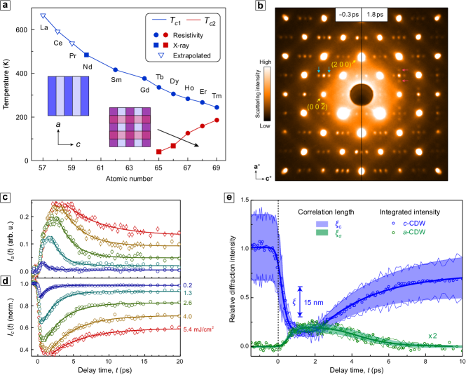
Te3 are layered van der Waals materials that crystallize in nearly tetragonal structures with only a slight anisotropy between the two in-plane axes, and [7]. All members share similar structural and electronic properties except for the different chemical pressures exerted by the rare-earth elements with varying ionic radii. As one moves from La to Tm, shown in Fig. 1(a), the material can host either a unidirectional CDW along the -axis or a bidirectional CDW along both in-plane axes. The critical temperatures of the respective transitions display opposite trends, suggesting a phase competition between the - and -axis CDWs. In equilibrium, the slight lattice anisotropy dictates that the -axis CDW always forms first. If this order is sufficiently strong, the -axis CDW cannot be stabilized under ambient pressure.
The Te3 family has been extensively studied by time-resolved optical spectroscopy [8, 9, 10, 11], photoemission [12, 13, 14, 15, 10, 16], X-ray scattering [17, 18, 19, 16], and electron diffraction [20, 10], providing a prototypical platform for investigating uniquely nonequilibrium phenomena associated with a photoinduced transition. However, most studies only concentrate on the dominant -axis CDW while neglecting the competing -axis order. Starting from the unidirectional CDW state in LaTe3, Kogar et al. found that while a femtosecond laser pulse suppressed the equilibrium -axis CDW, it also seeded the growth of the competing -axis order [5]. This light-induced CDW is evident from electron diffraction images taken before and after the incidence of the pump laser pulse, shown in Fig. 1(b), where blue and red arrows indicate pairs of CDW peaks along the and axes, respectively. The same observation was reported by Zhou et al. in CeTe3 [Fig. 1(e)] [6], and we expect other members of the Te3 family to exhibit similar phenomenology in their unidirectional CDW phase. The competing nature of the equilibrium and the light-induced CDWs is best illustrated by the evolution of their superlattice peak intensities, shown in Fig. 1(c,d). As photoexcitation quenches the -axis CDW peak within 400 fs, the -axis peak emerges at the same time. The slightly slower rise along the direction compared to the faster intensity drop in the direction hints at the incoherent development of the light-induced CDW in different spatial regions of the sample, in contrast to a coherent displacive motion that drives the melting of the equilibrium order. On the other hand, during the relaxation to a quasi-equilibrium plateau, the intensity curves are perfectly anti-correlated between the two CDWs for all pump fluences measured, suggesting a strong competition scenario.
There are a number of peculiarities observed in the light-induced CDW that warrant further research. For example, the modulation wavevector of the nonequilibrium -axis CDW appears to be distinct from the value of the equilibrium order in the checkerboard-like state [5], pointing towards a truly nonequilibrium state with no equilibrium counterpart. Furthermore, the dominant -axis modulation acquires a persistent wavevector shift that cannot be explained by laser-induced heating [6], further underscoring the nonthermal nature of the light-induced state. With improved momentum resolution, the correlation length of the photoinduced CDW can be more accurately quantified along different directions in future experiments, offering insights into whether the CDW can transiently acquire three-dimensional phase coherence, an important question with broad implications in other light-induced states. By tailoring the photoexcitation conditions, for instance by adjusting the pulse width, fluence, or even applying a particular pulse sequence, one could also engineer ways to prolong the lifetime of the light-induced order beyond just a few picoseconds [21].
II Electronic correlations
In materials with strong electronic correlations, charge is often coupled to the spin, orbital, or structural degrees of freedom. As many of these systems possess -electrons that sit close to the boundary between electron itinerancy and localization, there often exists a wide variety of phase transitions that can be triggered with small external perturbations [24]. Vanadium dioxide (VO2) is a prototypical example of such a material where, in thermal equilibrium, a high-temperature metallic phase gives way to a low-temperature insulating phase below K. Accompanying the orders-of-magnitude change in conductivity is a crystallographic phase transition from a high-temperature rutile to a low-temperature monoclinic structure. The transition has remained controversial for decades with researchers arguing about whether it is primarily driven by electron correlations or electron-phonon interactions [25]. Roughly two decades ago, it was found that a femtosecond laser pulse could instigate the transition between the two phases, evidenced by photoinduced changes in the optical response and diffraction peaks [26, 27, 28, 29], yielding new experimental insight into the transition in VO2.
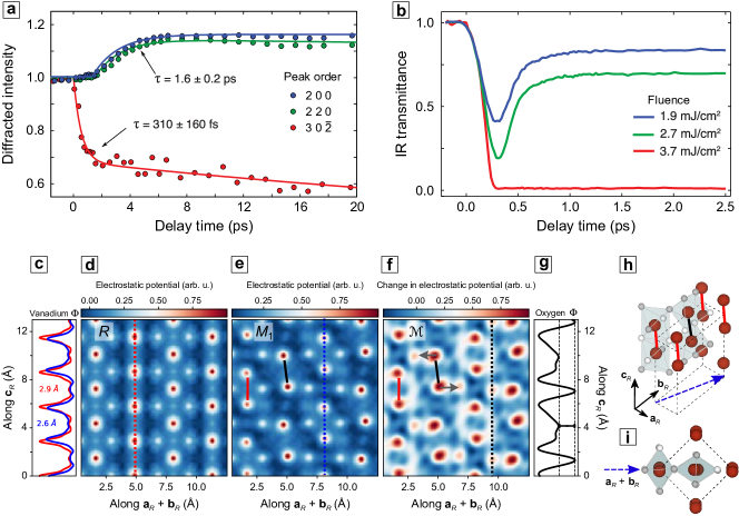
Recently, ultrafast electron diffraction has provided a fresh perspective concerning this particular transition through strong evidence of a metastable metallic phase with a monoclinic structure [22, 23, 30]. Of utmost importance in these studies is the sensitivity of low-angle electron diffraction peaks to the valence electron distribution. In contrast to scattering probes such as X-ray and neutron diffraction, electron diffraction is sensitive to the valence electron density in addition to the lattice structure [31]. This key detail allowed Otto et al. to determine the change in the electric potential and electronic distribution after photoexcitation with an 800 nm wavelength laser pulse [23].
Figure 2(a) shows that VO2 exhibits two diffraction timescales after photoexcitation at room temperature, depending on which peaks are examined. Faster timescales below 1 ps are associated with the crystallographic transformation to the rutile structure while the slow timescales over several picoseconds are assigned to the electronic redistribution. Remarkably, below a certain fluence threshold ( mJ/cm2), only the slow timescales are observed, indicating that the system retains its monoclinic structure. By also measuring the infrared transmissivity at a wavelength of 5 m [Fig. 2(b)], Siwick and coworkers were able to determine that this monoclinic phase is metallic by mJ/cm2. The electronic redistribution was estimated using the Patterson method based on the diffraction pattern, and is plotted in Fig. 2(d–f). In Fig. 2(d), the electrostatic potential of the equilibrium rutile phase () is shown, demonstrating that the high-symmetry phase consists of equally spaced vanadium atoms along the cR axis [red curve in Fig. 2(c)]; see Fig. 2(h,i) for the definition of crystalline axes. A similar plot for the equilibrium monoclinic phase () is shown in Fig. 2(e), where a clear dimerization of the vanadium atoms takes place [blue curve in Fig. 2(c)]. Figure 2(f) shows the change in the electric potential 10 ps after photoexcitation with a fluence of 6 mJ/cm2. Despite the reorganization of electrons, the vanadium atoms retain their dimerized structure. Interestingly, the electronic redistribution in the nonequilibrium metastable phase () discriminates between two oxygen atoms that are symmetry equivalent in the rutile phase, which is highlighted by the line cut through the oxygen atoms in Fig. 2(g).
There are still many open questions about this metallic monoclinic phase, but the data are suggestive that the rutile structure is not a necessary requirement for metallicity in this system. One question apparent from a comparison between Fig. 2(a) and (b) is that the infrared transmissivity has a timescale corresponding to the “fast” timescale in the diffraction peaks, although only the relatively slow transition into a monoclinic metallic phase is expected in transmissivity at fluences below mJ/cm2. While this and other issues abound, the metastable metallic phase with monoclinic structure represents a case study where ultrafast electron diffraction yielded profound insight into a phase transition that is commonly associated with electronic correlations. Importantly, the sensitivity of the probing electrons to the valence electron distribution is exclusively accessed with ultrafast electron diffraction.
III Excitation of coherent modes
In a broken-symmetry phase, coherent photoexcitation of a collective mode – be it a phonon, magnon, plasmon, or a hybrid – offers important clues about the ground state properties and associated phase transitions. Here, the word coherent means that microscopic entities such as lattice ions, charge or spin undergo a phase-locked motion over a macroscopic length scale. The synchronized motion typically manifests as an oscillatory signal when plotted against pump-probe time delay, and its amplitude and frequency encode information about the local environment in a highly excited medium. When several intertwined degrees of freedom are present, these coherent modes are particularly useful in isolating the driving force behind the formation of the ground state. If oscillations with the same frequency are detected in different observables, such as ionic position and electronic energy, these modes also allow a precise measurement of the coupling strength between various microscopic entities, free from interference of incoherent dynamics that are often too complex to model [32].
In the context of UED and UEM, the most readily detected coherent modes are phonons. Besides resonant driving through a terahertz or mid-infrared pulse [37], coherent optical phonons can be generated by impulsive stimulated Raman scattering [38], displacive excitation [39], or transient depletion field screening [40]. For coherent acoustic phonons, they may instead result from electron-phonon deformation potential, thermoelasticity, the inverse piezoelectric effect, electrostriction, and magnetostriction [41, 42]. Early studies of coherent phonons in UED were focused on elemental thin films such as aluminum [43], silicon [44], bismuth [45, 46], and graphite [47, 48], revealing important information such as the Grüneisen parameter of a material. Here, we review more recent studies in which coherent phonons are driven to large amplitude so that the initial harmonic motion can transform into a plastic distortion, giving rise to a long-lasting metastable state. Via a multi-pulse sequence, the coherent motion can also be amplified or suppressed with femtosecond precision, allowing one to manipulate the nonequilibrium pathway of a photoinduced transition.
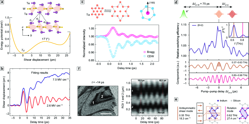
A notable example is the light-induced topological transition from a type-II Weyl semimetal to a normal semimetal in WTe2 [33]. As illustrated in Fig. 3(a), the transition originates from a shear motion between van der Waals-bonded layers, leading to a structural change from the noncentrosymmetric ground state towards a centrosymmetric orthorhombic 1 phase. In a UED experiment, the coherent shear mode was evidenced by a periodic modulation of the Bragg peak intensity. Through a structure factor calculation, Sie et al. were able to extract the exact atomic displacement down to picometer precision [Fig. 3(b)]. In the UED measurement, intense terahertz pulses were used (1.5 THz or 23 THz) to instigate the coherent shear mode, though excitation at higher photon energy up to 1.55 eV was shown to exhibit similar phenomenology [49]. For very high excitation field (7.5 MV/cm), the oscillatory motion starts to deviate from its equilibrium position and slowly morphs into a metastable state over 25 ps [blue curve in Fig. 3(b)]. This trend signifies a large-amplitude, anharmonic lattice motion that drives WTe2 into a new polytype, 1, which persists for more than 70 ps. As an independent check for the photoinduced symmetry switch, rotation anisotropy-second harmonic generation (RA-SHG) measurement was carried out before and after -WTe2 was photoexcited. The large RA-SHG signal from an inversion symmetry-broken state almost completely vanishes in all polarization channels upon photoexcitation, lending further support to a scenario that WTe2 enters a topologically trivial phase with restored inversion symmetry.
With significant progress in temporal resolution, coherent optical phonons with frequencies up to several terahertz can be resolved by UED at present. A special type of optical phonon is the amplitude mode of a CDW phase, which describes the atomic motion along the trajectory that connects the CDW and the high-temperature states. A hallmark of the amplitude mode is the anti-phase relation of intensity modulation between the CDW superlattice peak and the crystal Bragg peak, which was first visualized by UED in a paradigmatic CDW material, 1-TaS2 [Fig. 3(c)] [34]. In this case, the amplitude mode is a breathing motion of twelve Ta atoms surrounding a central Ta atom, which carries a characteristic frequency of 2.4 THz at 40 K. The use of UED is instrumental in this measurement because both Bragg and superlattice peaks need to be captured within the same detector frame to directly compare their phase relation in the oscillatory dynamics. At sufficiently high pumping fluence, it is possible that atoms traveling along their amplitude mode coordinate eventually “overshoot” across the high-symmetry position, entering an inverted CDW state. This scenario was first postulated in K0.3MoO3 [50] and subsequently proposed for SmTe3 [18] and 1-TaSe2 [51]. As the inversion only takes place above a threshold fluence, an intriguing possibility arises due to different absorbed fluences at different depths of the sample, leading to a domain wall between the normal and the inverted CDW states [9, 52, 19, 53]. This domain wall is shown to exist in classic CDW systems such as rare-earth tritellurides [9, 19] and 1-TiSe2 [53], and its generation is expected to be generic in other broken-symmetry states possessing an amplitude mode. As the CDW locally collapses at the domain wall, the persistent nature of the domain wall would allow the proliferation of other phases that compete with the equilibrium CDW, possibly leading to novel photoinduced orders.
Leveraging a well-defined frequency of a coherently excited phonon mode, one can further design a pulse sequence to achieve a surgical control over the photoinduced phase transition and the resulting metastable state. Horstmann et al. demonstrated such an example in atomic indium wires grown on the (111) surface of silicon [35]. At room temperature, the atomic wire is metallic and forms a superstructure. It undergoes a first-order Peierls-like transition into an insulating state upon cooling [54]. The reverse transition can be instigated by an ultrafast light pulse [55, 56, 35]; owing to the first-order character, the system can be trapped in a metastable state that persists over nanoseconds. Horstmann et al. studied this photoinduced transition with two pump pulses that are delayed by and recorded the excited structure with an electron pulse at 75 ps after the second pump pulse, when the system has already relaxed into the metastable phase [see schematic in Fig. 3(d)] [35]. It was discovered that the efficiency of switching from the ground state into the metastable phase sensitively depends on the pump-pump temporal separation, exhibiting a pronounced oscillation as is varied [Fig. 3(d)]. Based on the Fourier transform of the switching efficiency, two spectral components are found to be responsible for the oscillation, indicated by the brown and red curves in Fig. 3(d). They correspond to an antisymmetric shear mode and a rotational mode of the indium hexagons – shown in Fig. 3(e) – which constitute the principal atomic motions for the transition. The identification of these driving phonons allowed the authors to harness their long-lasting vibrational coherence for phase engineering, opening the possibility of targeting specific modes to steer the phase transition pathway.
The coherent atomic motion triggered by an ultrafast light pulse can also be directly visualized in real space through UEM. With sub-100-nm spatial resolution and sub-picosecond temporal resolution, UEM has played an instrumental role in studying the photo-generation and propagation of acoustic waves, which locally modify the strain and hence the electronic properties in a wide class of materials [47, 57, 36, 58, 59, 60, 61, 62, 63]. While UED obtains spatially averaged information that could contain multiple frequencies from several coherent modes, UEM is capable of identifying the spatial origins for individual components. For example, Zhang and Flannigan examined a mechanically exfoliated van der Waals material, 2-MoS2, where two bend contours [1 and 2 in Fig. 3(f)] are separated by a crystal step edge [36]. Due to the different layer numbers at positions 1 and 2, photoinduced strain waves traveling back and forth across the layers acquire different round-trip times, leading to a gradual dephasing of the oscillatory signal between the two regions [Fig. 3(f)]. This experiment also reminds us that realistic materials are often characterized by defects, terraces, step edges, layer twists, or wrinkles, so the spatial resolution afforded by UEM is critical for studying their effects on the light-induced states.
IV Defect generation
One of the central questions pertaining to phase transitions triggered with light concerns how these transitions differ from those in thermal equilibrium. In the past few years, it has become clear that light-triggered phase transitions can give rise to topological defects, even in materials where the density of defects is negligible in thermal equilibrium. Topological defects are characterized by a region in space where the amplitude of the order parameter vanishes at a “core”. Depending on the broken symmetry, these defects can be points, lines, domain walls or consist of more exotic order parameter textures [64]. Engineering these defects with light gives rise to the possibility of controlling material properties in a metastable fashion and realizing unconventional phase transitions that are not present in thermal equilibrium [65, 34, 66, 67, 68].
The importance of topological defects to nonequilibrium phase transitions was originally recognized in a cosmological context. Kibble predicted that cosmic strings would be left over from the rapid expansion of the early universe. Soon after, the idea was adapted by Zurek to look at phase transitions in a condensed matter setting where a rapid thermal quench from a high-temperature disordered state to a low-temperature ordered one would similarly give rise to topological defects. Quantitatively, Zurek suggested that the density of topological defects in the ordered phase would scale with the quench time, exhibiting characteristic critical exponents [69]. Although light-induced phase transitions are qualitatively different from thermal quenching transitions (in that photons are usually used to excite electrons to high energy scattering states), a variety of experiments suggest that topological defects may play a significant role in light-triggered phase transitions as well.
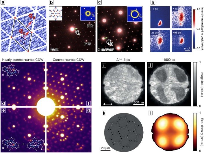
One of the best examples of light-induced defects is seen in the charge density wave state of 1-TaS2. This compound and its isovalent variants have been extensively studied by UED and UEM in recent years [2, 73, 74, 75, 76, 77, 78, 34, 71, 79, 80, 72]. Here, we restrict our discussion to cases where light-induced defects lead to newfound states of matter. In 2014, Stojchevska et al. suggested that defects were key to the stable and reversible control over an insulator-to-metal transition [65]. In this experiment, the authors used a single 1–3 mJ/cm2, 800 nm femtosecond light pulse to convert the low-temperature insulating state of 1-TaS2 into a “hidden” metastable metal. At temperatures below 4 K, the metallic state was present for over a week. A train of 10,000 subsequent pulses was then able to drive this metastable metal back into an insulator. Below 180 K, 1-TaS2 possesses a commensurate charge density wave, whose real space structure consists of tiled Star-of-David hexagrams with a superstructure [Fig. 3(c)]. The authors suggested that the metallicity arose out of ordered domain walls within this CDW texture, which has a configuration similar to that shown in Fig. 4(a). Subsequent electron diffraction studies, shown in Fig. 4(b,c), confirmed their suspicions. Figure 4(b) shows the equilibrium diffraction pattern in 1-TaS2 at 10 K, where superlattice peaks arising from commensurate charge density wave are easily visible. Once the system is photoexcited with a single pulse, the CDW peaks split into pairs of peaks along the CDW wavevector, characteristic of their predicted pattern of ordered domain walls. Although electron diffraction used in this way is not “ultrafast”, the physics demonstrated in this set of experiments is rather remarkable in the degree of control over the material properties. It should be emphasized that the “hidden” state is nowhere to be found on the equilibrium phase diagram and is thus a true nonequilibrium ordered state with no equilibrium counterpart [81, 82, 83].
These works on the “hidden” low-temperature state in 1-TaS2 have also spawned other experiments looking at the same material in different temperature regimes where 1-TaS2 possesses different phases. Notably, another qualitatively different switching phenomenon in 1-TaS2 was found in its room temperature nearly-commensurate (NC) CDW state. In equilibrium, the nearly-commensurate state consists again of commensurate patches separated by ordered domain walls. However, the ordering of the domain walls is completely different from that in the “hidden” state. In the NC-CDW state, CDW domains are roughly hexagonal, instead of the triangular ones observed in the “hidden” state, with larger regions of zero order parameter amplitude [84]. Of particular importance is that the NC-CDW state possesses broken mirror symmetry stemming from how the hexagrams are tiled. The inset of Fig. 4(e) shows the two possible domain orientations, which are labeled and . Zong et al. used a single mJ/cm2, 800 nm femtosecond light pulse to trigger a stable conversion to a qualitatively different diffraction pattern [34]. A single light pulse converted the diffraction pattern from that of Fig. 4(d) to that in Fig. 4(e). Again, the altered pattern was stable for an indefinite period of time. A subsequent identical pulse sent the diffraction pattern back into its original state [Fig. 4(d)]. At the moment, however, this switching behavior, unlike that in the “hidden” state, is not perfectly controllable. It is currently probabilistic in nature and sometimes only switches with the application of two or three pulses. Due to the stability of this new state at room temperature, the sample was examined with a conventional transmission electron microscope to map its real space texture. These latter studies revealed that the laser pulse had instigated the growth of domains of opposite mirror symmetry, which were separated by rigid domain walls, again demonstrating the importance of topological defects in changing the material properties in a metastable fashion. With both and domains present, the authors cooled the sample down into the commensurate CDW state, showing that the domains persisted and that the diffraction peaks get more intense [Fig. 4(g)]. At low temperatures, the kinetic barrier cannot be surmounted without damaging the sample, and it thus cannot be returned to its pristine state [Fig. 4(f)]. It remains to be seen whether the -domains can coexist with the metastable metallic “hidden” state, though there are no conceptual issues preventing such a “double metastability”.
Though the description of topological defects up to now have concentrated on their stability, other studies have focused on their dynamics. Using a newly developed technique, ultrafast low-energy electron diffraction (ULEED) with a nanometer-sized emission tip, Vogelgesang et al. measured the peak width in 1-TaS2 as a function of time after exciting the material from its nearly-commensurate state into an incommensurate state [71]. The low energy of the electrons (50–100 eV) permits a much better momentum resolution () compared to high-energy electron diffraction setups, making it possible to more accurately extract the correlation lengths of the CDW based on the peak width. In thermal equilibrium, the incommensurate state is present above room temperature at K. In their work, the authors found that the incommensurate peak width narrows as a function of time after photoexcitation, shown in Fig. 4(h), and they interpreted that the incommensurate phase is stabilized by the annihilation of topological defects. Such domain growth is referred to as domain coarsening, and the authors found a characteristic scaling behavior between the domain size and the time after photoexcitation, suggesting that such coarsening dynamics may be universal [85, 86]. These domain dynamics were further studied using an inhomogeneous excitation pulse profile [Fig. 4(l)] and imaged in real space using time-resolved dark-field microscopy with a tailor-made mask [Fig. 4(k)] [72]. Figure 4(i,j) shows the imaged sample before and after photoexcitation, where the incommensurate regions appear, interact, shrink, and then disappear. Although such methods currently do not have the spatial resolution to visualize individual defects, it seems like this may be possible in the future. Overall, these case studies present us with the view that topological defects are a key component in stabilizing thermodynamically inaccessible phases and in governing the kinetics of light-induced phase transitions. Ultrafast electron diffraction and microscopy will no doubt continue to play a significant role in the visualization of these defect dynamics.
V Conclusion and outlook
To realize a photoinduced state on demand, the most common tuning parameters in a UED/UEM experiment are pump photon flux, wavelength, polarization, pulse duration, and sample temperature. With advances in thin flake fabrication techniques, a current trend is to integrate more sophisticated perturbing fields that provide additional degrees of freedom to manipulate material properties in situ. A recent example is realized in the study of VO2 [30], where metal electrodes were patterned and deposited on a 60-nm-thick polycrystalline film via photolithography and electron-beam evaporation. This setup enables concurrent UED and transport measurements to characterize the photoinduced insulator-to-metal transition, and it further allows the application of an electrical pulse to trigger a similar metastable state. Another fruitful avenue is to incorporate a strain device that modifies the equilibrium lattice constants. It was recently shown that the two competing CDWs in Te3 can be selectively enhanced depending on the direction of an applied uniaxial stress [87], raising the intriguing question of whether the lifetime of the light-induced CDW can be adjusted by strain engineering. Although it is challenging to apply a significant stress on a nanometer-thick flake without buckling or sample damage, a strain device may be adopted in a ULEED setup for bulk crystals, as long as the stray electric field from the piezoelectric control is properly shielded from the low-energy electron probe.
If the photoinduced transition is irreversible or the metastable state does not relax before the arrival of the next pump pulse, a single-shot UED/UEM experiment is necessary. The leading challenge is to pack sufficient electrons within a single pulse without jeopardizing the spatiotemporal profile due to the space charge effect. Various schemes have been implemented in the past two decades [88, 89, 90, 91, 92, 93, 94] and most studies focus on the photoinduced melting of elemental films. With improved momentum resolution and signal-to-noise ratio, the single-shot scheme may be employed to answer more complex questions, such as solving the exact atomic trajectory towards the metastable “hidden” or “jammed” state in 1-TaS2 [65, 66].
To obtain real-space visualization of a photoinduced state, the dark-field imaging setup by Danz et al. may be extended to other systems [72]. However, the mask needs to be tailored for each sample and it requires precision positioning to sieve through diffraction peaks of interest. An area for development is to have an in situ programmable mask, in the same spirit as a spatial light modulator but for electrons instead. A crude implementation is to use a material with low melting point – such as elemental indium or bismuth – coated on a silicon nitride support film. The excitation pulse with an appropriate fluence may be focused to drill tiny holes on the metallic film to produce a diffraction mask, and subsequently the holes could be erased via a temperature cycle for repeated usage.
We also envision continued research effort on electron pulse compression to push towards sub-10-fs total resolution using, for example, particle accelerator technology [95, 96, 97, 98, 99]. In addition, improvements in signal-to-noise ratios can be leveraged to visualize diffuse signals away from Bragg peaks as described by Dürr et al. in this MRS Bulletin special issue [100]. These developments would enable the discovery of novel short-lived states, high-frequency collective modes, as well as unconventional pathways of energy transfer in an excited medium. Together, they would make UED and UEM indispensable tools for discovering and shaping nonequilibrium properties of matter.
Acknowledgments We acknowledge the support from Gordon and Betty Moore Foundation’s EPiQS Initiative grant GBMF9459 (manuscript writing). A.Z. acknowledges support from the Miller Institute for Basic Research in Science.
References
- de la Torre et al. [2021] A. de la Torre, D. M. Kennes, M. Claassen, S. Gerber, J. W. McIver, and M. A. Sentef, Nonthermal pathways to ultrafast control in quantum materials (2021), arXiv:2103.14888 .
- Eichberger et al. [2010] M. Eichberger, H. Schäfer, M. Krumova, M. Beyer, J. Demsar, H. Berger, G. Moriena, G. Sciaini, and R. J. D. Miller, Snapshots of cooperative atomic motions in the optical suppression of charge density waves, Nature 468, 799 (2010).
- Kaiser [2017] S. Kaiser, Light-induced superconductivity in high- cuprates, Phys. Scr. 92, 103001 (2017).
- Sun and Millis [2020] Z. Sun and A. J. Millis, Transient trapping into metastable states in systems with competing orders, Phys. Rev. X 10, 021028 (2020).
- Kogar et al. [2020] A. Kogar, A. Zong, P. E. Dolgirev, X. Shen, J. Straquadine, Y.-Q. Bie, X. Wang, T. Rohwer, I.-C. Tung, Y. Yang, R. Li, J. Yang, S. Weathersby, S. Park, M. E. Kozina, E. J. Sie, H. Wen, P. Jarillo-Herrero, I. R. Fisher, X. Wang, and N. Gedik, Light-induced charge density wave in LaTe3, Nat. Phys. 16, 159 (2020).
- Zhou et al. [2021] F. Zhou, J. Williams, S. Sun, C. D. Malliakas, M. G. Kanatzidis, A. F. Kemper, and C.-Y. Ruan, Nonequilibrium dynamics of spontaneous symmetry breaking into a hidden state of charge-density wave, Nat. Commun. 12, 566 (2021).
- Ru [2008] N. Ru, Charge Density Wave Formation in Rare-earth Tellurides, Ph.D. thesis, Stanford University, Stanford (2008).
- Yusupov et al. [2008] R. V. Yusupov, T. Mertelj, J. H. Chu, I. R. Fisher, and D. Mihailovic, Single-particle and collective mode couplings associated with 1- and 2-directional electronic ordering in metallic RTe3 (R=Ho, Dy, Tb), Phys. Rev. Lett. 101, 24602 (2008).
- Yusupov et al. [2010] R. Yusupov, T. Mertelj, V. V. Kabanov, S. Brazovskii, P. Kusar, J.-H. Chu, I. R. Fisher, and D. Mihailovic, Coherent dynamics of macroscopic electronic order through a symmetry breaking transition, Nat. Phys. 6, 681 (2010).
- Zong et al. [2019a] A. Zong, A. Kogar, Y.-Q. Bie, T. Rohwer, C. Lee, E. Baldini, E. Ergeçen, M. B. Yilmaz, B. Freelon, E. J. Sie, H. Zhou, J. Straquadine, P. Walmsley, P. E. Dolgirev, A. V. Rozhkov, I. R. Fisher, P. Jarillo-Herrero, B. V. Fine, and N. Gedik, Evidence for topological defects in a photoinduced phase transition, Nat. Phys. 15, 27 (2019a).
- Zong et al. [2019b] A. Zong, P. E. Dolgirev, A. Kogar, E. Ergeçen, M. B. Yilmaz, Y.-Q. Bie, T. Rohwer, I.-C. Tung, J. Straquadine, X. Wang, Y. Yang, X. Shen, R. Li, J. Yang, S. Park, M. C. Hoffmann, B. K. Ofori-Okai, M. E. Kozina, H. Wen, X. Wang, I. R. Fisher, P. Jarillo-Herrero, and N. Gedik, Dynamical slowing-down in an ultrafast photoinduced phase transition, Phys. Rev. Lett. 123, 097601 (2019b).
- Schmitt et al. [2008] F. Schmitt, P. S. Kirchmann, U. Bovensiepen, R. G. Moore, L. Rettig, M. Krenz, J.-H. Chu, N. Ru, L. Perfetti, D. H. Lu, M. Wolf, I. R. Fisher, and Z.-X. Shen, Transient electronic structure and melting of a charge density wave in TbTe3, Science 321, 1649 (2008).
- Schmitt et al. [2011] F. Schmitt, P. S. Kirchmann, U. Bovensiepen, R. G. Moore, J.-H. Chu, D. H. Lu, L. Rettig, M. Wolf, I. R. Fisher, and Z.-X. Shen, Ultrafast electron dynamics in the charge density wave material TbTe3, New J. Phys. 13, 063022 (2011).
- Leuenberger et al. [2015] D. Leuenberger, J. A. Sobota, S.-L. Yang, A. F. Kemper, P. Giraldo-Gallo, R. G. Moore, I. R. Fisher, P. S. Kirchmann, T. P. Devereaux, and Z.-X. Shen, Classification of collective modes in a charge density wave by momentum-dependent modulation of the electronic band structure, Phys. Rev. B 91, 201106 (2015).
- Rettig et al. [2016] L. Rettig, R. Cortés, J.-H. Chu, I. R. Fisher, F. Schmitt, R. G. Moore, Z.-X. Shen, P. S. Kirchmann, M. Wolf, and U. Bovensiepen, Persistent order due to transiently enhanced nesting in an electronically excited charge density wave, Nat. Commun. 7, 10459 (2016).
- Maklar et al. [2021] J. Maklar, Y. W. Windsor, C. W. Nicholson, M. Puppin, P. Walmsley, V. Esposito, M. Porer, J. Rittmann, D. Leuenberger, M. Kubli, M. Savoini, E. Abreu, S. L. Johnson, P. Beaud, G. Ingold, U. Staub, I. R. Fisher, R. Ernstorfer, M. Wolf, and L. Rettig, Nonequilibrium charge-density-wave order beyond the thermal limit, Nat. Commun. 12, 2499 (2021).
- Moore et al. [2016] R. G. Moore, W. S. Lee, P. S. Kirchman, Y. D. Chuang, A. F. Kemper, M. Trigo, L. Patthey, D. H. Lu, O. Krupin, M. Yi, D. A. Reis, D. Doering, P. Denes, W. F. Schlotter, J. J. Turner, G. Hays, P. Hering, T. Benson, J.-H. Chu, T. P. Devereaux, I. R. Fisher, Z. Hussain, and Z.-X. Shen, Ultrafast resonant soft X-ray diffraction dynamics of the charge density wave in TbTe3, Phys. Rev. B 93, 024304 (2016).
- Trigo et al. [2019] M. Trigo, P. Giraldo-Gallo, M. E. Kozina, T. Henighan, M. P. Jiang, H. Liu, J. N. Clark, M. Chollet, J. M. Glownia, D. Zhu, T. Katayama, D. Leuenberger, P. S. Kirchmann, I. R. Fisher, Z. X. Shen, and D. A. Reis, Coherent order parameter dynamics in SmTe3, Phys. Rev. B 99, 104111 (2019).
- Trigo et al. [2021] M. Trigo, P. Giraldo-Gallo, J. N. Clark, M. E. Kozina, T. Henighan, M. P. Jiang, M. Chollet, I. R. Fisher, J. M. Glownia, T. Katayama, P. S. Kirchmann, D. Leuenberger, H. Liu, D. A. Reis, Z. X. Shen, and D. Zhu, Ultrafast formation of domain walls of a charge density wave in SmTe3, Phys. Rev. B 103, 054109 (2021).
- Han et al. [2012] T.-R. T. Han, Z. Tao, S. D. Mahanti, K. Chang, C.-Y. Ruan, C. D. Malliakas, and M. G. Kanatzidis, Structural dynamics of two-dimensional charge-density waves in CeTe investigated by ultrafast electron crystallography, Phys. Rev. B 86, 075145 (2012).
- Budden et al. [2021] M. Budden, T. Gebert, M. Buzzi, G. Jotzu, E. Wang, T. Matsuyama, G. Meier, Y. Laplace, D. Pontiroli, M. Riccò, F. Schlawin, D. Jaksch, and A. Cavalleri, Evidence for metastable photo-induced superconductivity in K3C60, Nat. Phys. 17, 611 (2021).
- Morrison et al. [2014] V. R. Morrison, R. P. Chatelain, K. L. Tiwari, A. Hendaoui, A. Bruhács, M. Chaker, and B. J. Siwick, A photoinduced metal-like phase of monoclinic VO2 revealed by ultrafast electron diffraction, Science 346, 445 (2014).
- Otto et al. [2019] M. R. Otto, L. P. René de Cotret, D. A. Valverde-Chavez, K. L. Tiwari, N. Émond, M. Chaker, D. G. Cooke, and B. J. Siwick, How optical excitation controls the structure and properties of vanadium dioxide, Proc. Natl. Acad. Sci. U.S.A. 116, 450 (2019).
- Zhang and Averitt [2014] J. Zhang and R. Averitt, Dynamics and control in complex transition metal oxides, Annu. Rev. Mater. Res. 44, 19 (2014).
- Shao et al. [2018] Z. Shao, X. Cao, H. Luo, and P. Jin, Recent progress in the phase-transition mechanism and modulation of vanadium dioxide materials, NPG Asia Mater. 10, 581 (2018).
- Becker et al. [1996] M. F. Becker, A. B. Buckman, R. M. Walser, T. Lépine, P. Georges, and A. Brun, Femtosecond laser excitation dynamics of the semiconductor‐metal phase transition in VO2, J. Appl. Phys. 79, 2404 (1996).
- Cavalleri et al. [2001] A. Cavalleri, C. Tóth, C. W. Siders, J. A. Squier, F. Ráksi, P. Forget, and J. C. Kieffer, Femtosecond structural dynamics in VO2 during an ultrafast solid-solid phase transition, Phys. Rev. Lett. 87, 237401 (2001).
- Kim et al. [2006] H.-T. Kim, Y. W. Lee, B.-J. Kim, B.-G. Chae, S. J. Yun, K.-Y. Kang, K.-J. Han, K.-J. Yee, and Y.-S. Lim, Monoclinic and correlated metal phase in VO2 as evidence of the Mott transition: Coherent phonon analysis, Phys. Rev. Lett. 97, 266401 (2006).
- Baum et al. [2007] P. Baum, D.-S. Yang, and A. H. Zewail, 4D visualization of transitional structures in phase transformations by electron diffraction, Science 318, 788 (2007).
- Sood et al. [2021] A. Sood, X. Shen, Y. Shi, S. Kumar, S. J. Park, M. Zajac, Y. Sun, L.-Q. Chen, S. Ramanathan, X. Wang, W. C. Chueh, and A. M. Lindenberg, Universal phase dynamics in VO2 switches revealed by ultrafast operando diffraction, Science 373, 352 (2021).
- Zheng et al. [2005] J. C. Zheng, Y. Zhu, L. Wu, and J. W. Davenport, On the sensitivity of electron and X-ray scattering factors to valence charge distributions, J. Appl. Cryst. 38, 648 (2005).
- Gerber et al. [2017] S. Gerber, S.-L. Yang, D. Zhu, H. Soifer, J. a. Sobota, S. Rebec, J. J. Lee, T. Jia, B. Moritz, C. Jia, A. Gauthier, Y. Li, D. Leuenberger, Y. Zhang, L. Chaix, W. Li, H. Jang, J.-S. Lee, M. Yi, G. L. Dakovski, S. Song, J. M. Glownia, S. Nelson, K. W. Kim, Y.-D. Chuang, Z. Hussain, R. G. Moore, T. P. Devereaux, W.-S. Lee, P. S. Kirchmann, and Z.-X. Shen, Femtosecond electron-phonon lock-in by photoemission and x-ray free-electron laser, Science 357, 71 (2017).
- Sie et al. [2019] E. J. Sie, C. M. Nyby, C. D. Pemmaraju, S. J. Park, X. Shen, J. Yang, M. C. Hoffmann, B. K. Ofori-Okai, R. Li, A. H. Reid, S. Weathersby, E. Mannebach, N. Finney, D. Rhodes, D. Chenet, A. Antony, L. Balicas, J. Hone, T. P. Devereaux, T. F. Heinz, X. Wang, and A. M. Lindenberg, An ultrafast symmetry switch in a Weyl semimetal, Nature 565, 61 (2019).
- Zong et al. [2018] A. Zong, X. Shen, A. Kogar, L. Ye, C. Marks, D. Chowdhury, T. Rohwer, B. Freelon, S. Weathersby, R. Li, J. Yang, J. Checkelsky, X. Wang, and N. Gedik, Ultrafast manipulation of mirror domain walls in a charge density wave, Sci. Adv. 4, eaau5501 (2018).
- Horstmann et al. [2020] J. G. Horstmann, H. Böckmann, B. Wit, F. Kurtz, G. Storeck, and C. Ropers, Coherent control of a surface structural phase transition, Nature 583, 232 (2020).
- Zhang and Flannigan [2019] Y. Zhang and D. J. Flannigan, Observation of anisotropic strain-wave dynamics and few-layer dephasing in MoS2 with ultrafast electron microscopy, Nano Lett. 19, 8216 (2019).
- Subedi et al. [2014] A. Subedi, A. Cavalleri, and A. Georges, Theory of nonlinear phononics for coherent light control of solids, Phys. Rev. B 89, 220301 (2014).
- Stevens et al. [2002] T. E. Stevens, J. Kuhl, and R. Merlin, Coherent phonon generation and the two stimulated Raman tensors, Phys. Rev. B 65, 144304 (2002).
- Zeiger et al. [1992] H. J. Zeiger, J. Vidal, T. K. Cheng, E. P. Ippen, G. Dresselhaus, and M. S. Dresselhaus, Theory for displacive excitation of coherent phonons, Phys. Rev. B 45, 768 (1992).
- Först and Dekorsy [2007] M. Först and T. Dekorsy, Coherent phonons in bulk and low-dimensional semiconductors, in Coherent Vibrational Dynamics, edited by G. Lanzani, G. Cerullo, and S. De Silvestri (CRC Press, Boca Raton, 2007) pp. 129–172.
- Ruello and Gusev [2015] P. Ruello and V. E. Gusev, Physical mechanisms of coherent acoustic phonons generation by ultrafast laser action, Ultrasonics 56, 21 (2015).
- Korff Schmising et al. [2008] C. V. Korff Schmising, A. Harpoeth, N. Zhavoronkov, Z. Ansari, C. Aku-Leh, M. Woerner, T. Elsaesser, M. Bargheer, M. Schmidbauer, I. Vrejoiu, D. Hesse, and M. Alexe, Ultrafast magnetostriction and phonon-mediated stress in a photoexcited ferromagnet, Phys. Rev. B 78, 060404 (2008).
- Nie et al. [2006] S. Nie, X. Wang, H. Park, R. Clinite, and J. Cao, Measurement of the electronic Grüneisen constant using femtosecond electron diffraction, Phys. Rev. Lett. 96, 15 (2006).
- Harb et al. [2009] M. Harb, W. Peng, G. Sciaini, C. T. Hebeisen, R. Ernstorfer, M. A. Eriksson, M. G. Lagally, S. G. Kruglik, and R. J. D. Miller, Excitation of longitudinal and transverse coherent acoustic phonons in nanometer free-standing films of (001) Si, Phys. Rev. B 79, 094301 (2009).
- Bugayev et al. [2011] A. Bugayev, A. Esmail, M. Abdel-Fattah, and H. E. Elsayed-Ali, Coherent phonons in bismuth film observed by ultrafast electron diffraction, AIP Adv. 1, 012117 (2011).
- Moriena et al. [2012] G. Moriena, M. Hada, G. Sciaini, J. Matsuo, and R. J. Dwayne Miller, Femtosecond electron diffraction: Preparation and characterization of (110)-oriented bismuth films, J. Appl. Phys. 111, 043504 (2012).
- Park et al. [2009] H. S. Park, J. S. Baskin, B. Barwick, O.-H. Kwon, and A. H. Zewail, 4D ultrafast electron microscopy: Imaging of atomic motions, acoustic resonances, and moiré fringe dynamics, Ultramicroscopy 110, 7 (2009).
- Chatelain et al. [2014] R. P. Chatelain, V. R. Morrison, B. L. M. Klarenaar, and B. J. Siwick, Coherent and incoherent electron-phonon coupling in graphite observed with radio-frequency compressed ultrafast electron diffraction, Phys. Rev. Lett. 113, 235502 (2014).
- Zhang et al. [2019] M. Y. Zhang, Z. X. Wang, Y. N. Li, L. Y. Shi, D. Wu, T. Lin, S. J. Zhang, Y. Q. Liu, Q. M. Liu, J. Wang, T. Dong, and N. L. Wang, Light-induced subpicosecond lattice symmetry switch in MoTe2, Phys. Rev. X 9, 021036 (2019).
- Huber et al. [2014] T. Huber, S. O. Mariager, A. Ferrer, H. Schäfer, J. A. Johnson, S. Grübel, A. Lübcke, L. Huber, T. Kubacka, C. Dornes, C. Laulhe, S. Ravy, G. Ingold, P. Beaud, J. Demsar, and S. L. Johnson, Coherent structural dynamics of a prototypical charge-density-wave-to-metal transition, Phys. Rev. Lett. 113, 026401 (2014).
- Zhang et al. [2020] Y. Zhang, X. Shi, M. Guan, W. You, Y. Zhong, T. R. Kafle, Y. Huang, H. Ding, M. Bauer, K. Rossnagel, S. Meng, H. C. Kapteyn, and M. M. Murnane, Creation of a novel inverted charge density wave state (2020), arXiv:2011.07623 .
- Wang and Wang [2019] Y. Wang and D. Wang, Writing and erasing topological defects in charge density wave materials with femtosecond laser pulses, Opt. Lett. 44, 2939 (2019).
- Duan et al. [2021] S. Duan, Y. Cheng, W. Xia, Y. Yang, C. Xu, F. Qi, C. Huang, T. Tang, Y. Guo, W. Luo, D. Qian, D. Xiang, J. Zhang, and W. Zhang, Optical manipulation of electronic dimensionality in a quantum material, Nature 595, 239 (2021).
- Snijders and Weitering [2010] P. C. Snijders and H. H. Weitering, Colloquium: Electronic instabilities in self-assembled atom wires, Rev. Mod. Phys. 82, 307 (2010).
- Wall et al. [2012] S. Wall, B. Krenzer, S. Wippermann, S. Sanna, F. Klasing, A. Hanisch-Blicharski, M. Kammler, W. G. Schmidt, and M. Horn-von Hoegen, Atomistic Picture of Charge Density Wave Formation at Surfaces, Phys. Rev. Lett. 109, 186101 (2012).
- Frigge et al. [2017] T. Frigge, B. Hafke, T. Witte, B. Krenzer, C. Streubühr, A. Samad Syed, V. Mikšić Trontl, I. Avigo, P. Zhou, M. Ligges, D. von der Linde, U. Bovensiepen, M. Horn-von Hoegen, S. Wippermann, A. Lücke, S. Sanna, U. Gerstmann, and W. G. Schmidt, Optically excited structural transition in atomic wires on surfaces at the quantum limit, Nature 544, 207 (2017).
- Zewail [2010] A. H. Zewail, Four-Dimensional Electron Microscopy, Science 328, 187 (2010).
- Cremons et al. [2016] D. R. Cremons, D. A. Plemmons, and D. J. Flannigan, Femtosecond electron imaging of defect-modulated phonon dynamics, Nat. Commun. 7, 11230 (2016).
- McKenna et al. [2017] A. J. McKenna, J. K. Eliason, and D. J. Flannigan, Spatiotemporal evolution of coherent elastic strain waves in a single MoS2 flake, Nano Lett. 17, 3952 (2017).
- Feist et al. [2018] A. Feist, N. Rubiano da Silva, W. Liang, C. Ropers, and S. Schäfer, Nanoscale diffractive probing of strain dynamics in ultrafast transmission electron microscopy, Struct. Dynam. 5, 014302 (2018).
- Kim et al. [2019a] Y.-J. Kim, H. Jung, S. W. Han, and O.-H. Kwon, Ultrafast electron microscopy visualizes acoustic vibrations of plasmonic nanorods at the interfaces, Matter 1, 481 (2019a).
- Nakamura et al. [2020] A. Nakamura, T. Shimojima, Y. Chiashi, M. Kamitani, H. Sakai, S. Ishiwata, H. Li, and K. Ishizaka, Nanoscale imaging of unusual photoacoustic waves in thin flake VTe2, Nano Lett. 20, 4932 (2020).
- Kim et al. [2020] Y.-J. Kim, Y. Lee, K. Kim, and O.-H. Kwon, Light-induced anisotropic morphological dynamics of black phosphorus membranes visualized by dark-field ultrafast electron microscopy, ACS Nano 14, 11383 (2020).
- Srivastava [2001] A. M. Srivastava, Topological defects in condensed matter physics, in Field Theories in Condensed Matter Physics (Hindustan Book Agency, Gurgaon, 2001) pp. 189–237.
- Stojchevska et al. [2014] L. Stojchevska, I. Vaskivskyi, T. Mertelj, P. Kusar, D. Svetin, S. Brazovskii, and D. Mihailovic, Ultrafast switching to a stable hidden quantum state in an electronic crystal, Science 344, 177 (2014).
- Gerasimenko et al. [2019] Y. A. Gerasimenko, I. Vaskivskyi, M. Litskevich, J. Ravnik, J. Vodeb, M. Diego, V. Kabanov, and D. Mihailovic, Quantum jamming transition to a correlated electron glass in 1T-TaS2, Nat. Mater. 18, 1078 (2019).
- Stoica et al. [2019] V. A. Stoica, N. Laanait, C. Dai, Z. Hong, Y. Yuan, Z. Zhang, S. Lei, M. R. McCarter, A. Yadav, A. R. Damodaran, S. Das, G. A. Stone, J. Karapetrova, D. A. Walko, X. Zhang, L. W. Martin, R. Ramesh, L.-Q. Chen, H. Wen, V. Gopalan, and J. W. Freeland, Optical creation of a supercrystal with three-dimensional nanoscale periodicity, Nat. Mater. 18, 377 (2019).
- Büttner et al. [2021] F. Büttner, B. Pfau, M. Böttcher, M. Schneider, G. Mercurio, C. M. Günther, P. Hessing, C. Klose, A. Wittmann, K. Gerlinger, L.-M. Kern, C. Strüber, C. von Korff Schmising, J. Fuchs, D. Engel, A. Churikova, S. Huang, D. Suzuki, I. Lemesh, M. Huang, L. Caretta, D. Weder, J. H. Gaida, M. Möller, T. R. Harvey, S. Zayko, K. Bagschik, R. Carley, L. Mercadier, J. Schlappa, A. Yaroslavtsev, L. Le Guyarder, N. Gerasimova, A. Scherz, C. Deiter, R. Gort, D. Hickin, J. Zhu, M. Turcato, D. Lomidze, F. Erdinger, A. Castoldi, S. Maffessanti, M. Porro, A. Samartsev, J. Sinova, C. Ropers, J. H. Mentink, B. Dupé, G. S. D. Beach, and S. Eisebitt, Observation of fluctuation-mediated picosecond nucleation of a topological phase, Nat. Mater. 20, 30 (2021).
- Kibble [2007] T. Kibble, Phase-transition dynamics in the lab and the universe, Phys. Today 60, 47 (2007).
- Sun et al. [2018] K. Sun, S. Sun, C. Zhu, H. Tian, H. Yang, and J. Li, Hidden CDW states and insulator-to-metal transition after a pulsed femtosecond laser excitation in layered chalcogenide 1-TaS2-xSex, Sci. Adv. 4, eaas9660 (2018).
- Vogelgesang et al. [2018] S. Vogelgesang, G. Storeck, J. G. Horstmann, T. Diekmann, M. Sivis, S. Schramm, K. Rossnagel, S. Schäfer, and C. Ropers, Phase ordering of charge density waves traced by ultrafast low-energy electron diffraction, Nat. Phys. 14, 184 (2018).
- Danz et al. [2021] T. Danz, T. Domröse, and C. Ropers, Ultrafast nanoimaging of the order parameter in a structural phase transition, Science 371, 371 (2021).
- Erasmus et al. [2012] N. Erasmus, M. Eichberger, K. Haupt, I. Boshoff, G. Kassier, R. Birmurske, H. Berger, J. Demsar, and H. Schwoerer, Ultrafast dynamics of charge density waves in 4-TaSe2 probed by femtosecond electron diffraction, Phys. Rev. Lett. 109, 1 (2012).
- Sun et al. [2015] S. Sun, L. Wei, Z. Li, G. Cao, Y. Liu, W. J. Lu, Y. P. Sun, H. Tian, H. Yang, and J. Li, Direct observation of an optically induced charge density wave transition in 1-TaSe2, Phys. Rev. B 92, 224303 (2015).
- Han et al. [2015] T.-R. T. Han, F. Zhou, C. D. Malliakas, P. M. Duxbury, S. D. Mahanti, M. G. Kanatzidis, and C.-Y. Ruan, Exploration of metastability and hidden phases in correlated electron crystals visualized by femtosecond optical doping and electron crystallography, Sci. Adv. 1, e1400173 (2015).
- Haupt et al. [2016] K. Haupt, M. Eichberger, N. Erasmus, A. Rohwer, J. Demsar, K. Rossnagel, and H. Schwoerer, Ultrafast metamorphosis of a complex charge-density wave, Phys. Rev. Lett. 116, 016402 (2016).
- Wei et al. [2017] L. Wei, S. Sun, C. Guo, Z. Li, K. Sun, Y. Liu, W. Lu, Y. Sun, H. Tian, H. Yang, and J. Li, Dynamic diffraction effects and coherent breathing oscillations in ultrafast electron diffraction in layered 1-TaSeTe, Struct. Dynam. 4, 044012 (2017).
- Le Guyader et al. [2017] L. Le Guyader, T. Chase, A. H. Reid, R. K. Li, D. Svetin, X. Shen, T. Vecchione, X. J. Wang, D. Mihailovic, and H. A. Dürr, Stacking order dynamics in the quasi-two-dimensional dichalcogenide 1-TaS2 probed with MeV ultrafast electron diffraction, Struct. Dynam. 4, 044020 (2017).
- Li et al. [2019] J. Li, J. Li, K. Sun, L. Wu, H. Huang, R. Li, J. Yang, X. Shen, X. Wang, H. Luo, R. J. Cava, I. K. Robinson, Y. Zhu, W. Yin, and J. Tao, Ultrafast decoupling of atomic sublattices in a charge-density-wave material (2019), arXiv:1903.09911 .
- Ji et al. [2020] S. Ji, O. Grånäs, K. Rossnagel, and J. Weissenrieder, Transient three-dimensional structural dynamics in 1-TaSe2, Phys. Rev. B 101, 094303 (2020).
- Vaskivskyi et al. [2015] I. Vaskivskyi, J. Gospodaric, S. Brazovskii, D. Svetin, P. Sutar, E. Goreshnik, I. A. Mihailovic, T. Mertelj, and D. Mihailovic, Controlling the metal-to-insulator relaxation of the metastable hidden quantum state in 1-TaS2, Sci. Adv. 1, e1500168 (2015).
- Cho et al. [2016] D. Cho, S. Cheon, K.-S. Kim, S.-H. Lee, Y.-H. Cho, S.-W. Cheong, and H. W. Yeom, Nanoscale manipulation of the Mott insulating state coupled to charge order in 1T-TaS2, Nat. Commun. 7, 10453 (2016).
- Ma et al. [2016] L. Ma, C. Ye, Y. Yu, X. F. Lu, X. Niu, S. Kim, D. Feng, D. Tománek, Y.-W. Son, X. H. Chen, and Y. Zhang, A metallic mosaic phase and the origin of Mott-insulating state in 1T-TaS2, Nat. Commun. 7, 10956 (2016).
- Spijkerman et al. [1997] A. Spijkerman, J. L. de Boer, A. Meetsma, G. A. Wiegers, and S. van Smaalen, X-ray crystal-structure refinement of the nearly commensurate phase of 1-TaS2 in -dimensional superspace, Phys. Rev. B 56, 13757 (1997).
- Laulhé et al. [2017] C. Laulhé, T. Huber, G. Lantz, A. Ferrer, S. O. Mariager, S. Grübel, J. Rittmann, J. A. Johnson, V. Esposito, A. Lübcke, L. Huber, M. Kubli, M. Savoini, V. L. R. Jacques, L. Cario, B. Corraze, E. Janod, G. Ingold, P. Beaud, S. L. Johnson, and S. Ravy, Ultrafast formation of a charge density wave state in 1-TaS2: Observation at nanometer scales using time-resolved x-ray diffraction, Phys. Rev. Lett. 118, 247401 (2017).
- Bray [1994] A. J. Bray, Theory of phase-ordering kinetics, Adv. Phys. 43, 357 (1994).
- Straquadine et al. [2020] J. A. W. Straquadine, M. S. Ikeda, and I. R. Fisher, Evidence for realignment of the charge density wave state in ErTe3 and TmTe3 under uniaxial stress via elastocaloric and elastoresistivity measurements (2020), arXiv:2005.10461 .
- Siwick et al. [2003] B. J. Siwick, J. R. Dwyer, R. E. Jordan, and R. J. D. Miller, An Atomic-Level View of Melting Using Femtosecond Electron Diffraction, Science 302, 1382 (2003).
- Sciaini et al. [2009] G. Sciaini, M. Harb, S. G. Kruglik, T. Payer, C. T. Hebeisen, F.-J. M. Z. Heringdorf, M. Yamaguchi, M. H.-v. Hoegen, R. Ernstorfer, and R. J. D. Miller, Electronic acceleration of atomic motions and disordering in bismuth, Nature 458, 56 (2009).
- Tokita et al. [2010] S. Tokita, M. Hashida, S. Inoue, T. Nishoji, K. Otani, and S. Sakabe, Single-Shot Femtosecond Electron Diffraction with Laser-Accelerated Electrons: Experimental Demonstration of Electron Pulse Compression, Phys. Rev. Lett. 105, 215004 (2010).
- Musumeci et al. [2010] P. Musumeci, J. T. Moody, C. M. Scoby, M. S. Gutierrez, H. A. Bender, and N. S. Wilcox, High quality single shot diffraction patterns using ultrashort megaelectron volt electron beams from a radio frequency photoinjector, Rev. Sci. Instrum. 81, 013306 (2010).
- Li et al. [2010] R. Li, W. Huang, Y. Du, L. Yan, Q. Du, J. Shi, J. Hua, H. Chen, T. Du, H. Xu, and C. Tang, Note: Single-shot continuously time-resolved MeV ultrafast electron diffraction, Rev. Sci. Instrum. 81, 036110 (2010).
- Speirs et al. [2015] R. W. Speirs, C. T. Putkunz, A. J. McCulloch, K. A. Nugent, B. M. Sparkes, and R. E. Scholten, Single-shot electron diffraction using a cold atom electron source, J. Phys. B 48, 214002 (2015), 1506.07442 .
- Mo et al. [2018] M. Z. Mo, Z. Chen, R. K. Li, M. Dunning, B. B. L. Witte, J. K. Baldwin, L. B. Fletcher, J. B. Kim, A. Ng, R. Redmer, A. H. Reid, P. Shekhar, X. Z. Shen, M. Shen, K. Sokolowski-Tinten, Y. Y. Tsui, Y. Q. Wang, Q. Zheng, X. J. Wang, and S. H. Glenzer, Heterogeneous to homogeneous melting transition visualized with ultrafast electron diffraction, Science 360, 1451 (2018).
- Wang et al. [1996] X. J. Wang, X. Qiu, and I. Ben-Zvi, Experimental observation of high-brightness microbunching in a photocathode rf electron gun, Phys. Rev. E 54, R3121 (1996).
- Wang et al. [2003] X. J. Wang, Z. Wu, and H. Ihee, Femto-seconds electron beam diffraction using photocathode RF gun, in Proc. 2003 Part. Accel. Conf., Vol. 1 (IEEE, 2003) pp. 420–422.
- Weathersby et al. [2015] S. P. Weathersby, G. Brown, M. Centurion, T. F. Chase, R. Coffee, J. Corbett, J. P. Eichner, J. C. Frisch, A. R. Fry, M. Gühr, N. Hartmann, C. Hast, R. Hettel, R. K. Jobe, E. N. Jongewaard, J. R. Lewandowski, R. K. Li, A. M. Lindenberg, I. Makasyuk, J. E. May, D. McCormick, M. N. Nguyen, A. H. Reid, X. Shen, K. Sokolowski-Tinten, T. Vecchione, S. L. Vetter, J. Wu, J. Yang, H. A. Dürr, and X. J. Wang, Mega-electron-volt ultrafast electron diffraction at SLAC National Accelerator Laboratory, Rev. Sci. Instrum. 86, 073702 (2015).
- Kim et al. [2019b] H. W. Kim, N. A. Vinokurov, I. H. Baek, K. Y. Oang, M. H. Kim, Y. C. Kim, K. H. Jang, K. Lee, S. H. Park, S. Park, J. Shin, J. Kim, F. Rotermund, S. Cho, T. Feurer, and Y. U. Jeong, Towards jitter-free ultrafast electron diffraction technology, Nat. Photon. 14, 245 (2019b).
- Qi et al. [2020] F. Qi, Z. Ma, L. Zhao, Y. Cheng, W. Jiang, C. Lu, T. Jiang, D. Qian, Z. Wang, W. Zhang, P. Zhu, X. Zou, W. Wan, D. Xiang, and J. Zhang, Breaking 50 femtosecond resolution barrier in MeV ultrafast electron diffraction with a double bend achromat compressor, Phys. Rev. Lett. 124, 134803 (2020).
- Dürr et al. [2021] H. A. Dürr, R. Ernstorfer, and B. J. Siwick, Revealing momentum-dependent electron–phonon and phonon–phonon coupling in complex materials with ultrafast electron diffuse scattering, MRS Bull. 46, 731 (2021).