Electronic structure and optical properties of Na2KSb and NaK2Sb from first-principles many-body theory
Abstract
In the search for novel materials for vacuum electron sources, multi-alkali antimonides and in particular sodium-potassium-antimonides have been recently regarded as especially promising due to their favorable electronic and optical properties. In the framework of density-functional theory and many-body perturbation theory, we investigate the electronic structure and the dielectric response of two representative members of this family, namely Na2KSb and NaK2Sb. We find that both materials have a direct gap, which is on the order of 1.5 eV in Na2KSb and 1.0 eV in NaK2Sb. In either system, valence and conduction bands are dominated by Sb states with - and -character, respectively. The imaginary part of the dielectric function, computed upon explicit inclusion of electron-hole interactions to characterize the optical response of the materials, exhibits maxima starting from the near-infrared region, extending up to the visible and the ultraviolet band. With our analysis, we clarify that the lowest-energy excitations are non-excitonic in nature and that their binding energy is on the order of 100 meV. Our results confirm the potential of Na2KSb and NaK2Sb as photoemissive materials for vacuum electron sources, photomultipliers, and imaging devices.
I Introduction
Multi-alkali antimonides comprise an interesting class of semiconducting compounds that have become popular for use as vacuum electron sources at particle accelerators, due to their favorable electronic properties [1, 2, 3]. Compared to conventional metals such as copper, which have been employed for decades to build photocathodes, alkali antimonides offer several advantages that are key for the development of the next generation of electron sources [3]. Their absorption onset in the visible region and their photoemission threshold at infrared frequencies ideally match the operational conditions of photocathodes illuminated by green laser pulses [3, 4]. These characteristics prevent inefficient energy conversion processes and together with the intrinsically low thermal emittance exhibited by semiconductors maximize the quantum efficiency of the cathode [5], which, posed in simple terms, represents the amount of emitted photoelectrons with respect to the amount of incident photons. Recent efforts of several groups worldwide have demonstrated the superiority of multi-alkali antimonides in terms of both quantum efficiency and mean transverse emittance (roughly speaking, the size of the emitted electron beam) [6, 7, 8, 9, 10, 11, 12, 13, 14, 15, 4] also in comparison with more widely studied semiconductors like GaAs [16, 17, 18].
From the experimental perspective, the routinely adopted deposition methods [19, 20, 21], together with the propensity of multi-alkali antimonides to be contaminated by atmospheric pollutants [11], demand ultrahigh vacuum conditions for both growth and characterization [22, 23] which minimize opportunities for thorough analysis. In light of these limitations, results of ab initio calculations represent a valuable source to obtain information about the properties of these systems. The pioneering studies by Ettema and de Groot [24, 25], based on the localized spherical wave method, demonstrated the potential of multi-alkali antimonides as photocathode materials. More recently, a few works based on density-functional theory (DFT) provided additional references to the electronic structure of this family of compounds [26, 27, 28, 29]. An important step forward, going beyond the mean-field picture of DFT, was offered by recent studies on Cs-based multi-alkali antimonides [30, 31]. The explicit inclusion of electron-electron and electron-hole interactions in the framework of many-body perturbation theory (MBPT) on top of DFT improves the accuracy in the description of the microscopic characteristics of these materials. Quantitative estimates of the fundamental and optical gaps and insight regarding the nature and composition of the lowest-energy excitations are essential quantities to subsequently evaluate the performance of a photocahode. To this end, the three-step model for photoemission, originally developed by Berglund and Spicer [32], is still largely applied and the very recent generalization to embed DFT results [33] opens promising perspectives to predict operational characteristics of photocathodes based on microscopic properties computed from first principles.
Research on multi-alkali antimonides has been so far mainly devoted to Cs-based compounds [8, 10, 34, 14, 15, 4]. However, interest is growing also towards the Na-based members of this family [35, 36, 19, 23, 37], reviving the predictions of early studies [38, 39, 40]. The higher electronegativity and lower atomic weight of sodium compared to heavier alkali metals such as cesium is expected to give rise to more advantageous characteristics for photocathode applications. In particular, their tolerance for high temperatures up to 200∘ and lower dark current is particularly appealing in particle accelerators. However, the realization of this high potential is hindered by the current lack of systematic studies, both theoretical and experimental, which can unravel and, most importantly, rationalize the microscopic physical properties of Na-based multi-alkali antimonides.
With this ab initio study based on DFT and MBPT, we aim to characterize the electronic and optical properties of Na2KSb and NaK2Sb, in order to provide reliable references for the development of Na-based antimonides as photocathode materials. To this end, we focus our analysis on the band structures of the systems, unraveling nature and size of the fundamental gaps, and inspecting the character of the valence and conduction states that are prominently involved in the photoabsorption and emission processes. Moreover, from the calculation of the dielectric function including explicitly electron-electron and electron-hole interactions, we gain insight into the energies and composition of the optical excitations.
This paper is organized as follows. In Section II, we review the adopted DFT and MBPT formalism and provide the relevant computational details. In Section III, the body of results are presented, including structural properties of Na2KSb and NaK2Sb (Section III.1), electronic structure (Section III.2), and optical excitations (Section III.3). In Section IV we summarize our findings and report our conclusions.
II Theoretical Background and Computational Details
The results presented in this work are performed in the framework of DFT [41] and MBPT including the approximation and the solution of the BSE [42]. The main task of DFT is the solution of the Kohn-Sham (KS) equations [43], where the accuracy of the results depends on the chosen approximation for the exchange-correlation (xc) potential.
In order to obtain a reliable description of the excited-state properties of the materials, MBPT is applied on top of the DFT band structure. In the approximation [44], the quasi-particle (QP) equation is solved to obtain electronic energies including the self-energy contribution. For this purpose, the single-shot approach [45] is adopted here. Optical excitations are calculated on top of the QP band structure from the solution of the BSE [46]. In practice, this problem is mapped into the eigenvalue equation
| (1) |
where for a spin-degenerate system the BSE Hamiltonian is expressed as : The diagonal term, , accounts for the transition energies between QP states; the direct Coulomb integral, , includes the screened electron-hole interaction; the exchange term, , incorporates the short-range repulsive exchange interaction. For further details about the formalism we refer the readers to specialized reviews [42, 47].
The eigenvalues of Eq. (1) correspond to the excitation energies while the eigenvectors provide information about the character of the excited states and their composition in terms of single-particle transitions. They enter the expression of the imaginary part of the macroscopic dielectric function
| (2) |
where is the unit cell volume and the frequency of the incoming photon, through the transition coefficients
| (3) |
Eq. (2) describes the optical response of the system. In cubic crystals, off-diagonal components are zero and the diagonal ones all bear the same value. In hexagonal crystals, two diagonal components are mutually equal and different from the third one. Macroscopic quantities, such as absorbance or reflectance can be obtained from the dielectric tensor [48], even in case of complex anisotropic crystals [49, 50, 51, 52].
Calculations are performed with the all-electron full-potential code exciting [53], which implements the linearised augmented plane wave plus local orbital formalism. This code offers a state-of-the-art implementation of MBPT, treating optical and core spectroscopy on equal footing [54, 47]. The muffin-tin radii of Na and K atoms are set to 2.0 bohr, while the radius of Sb to 2.2 bohr. A plane-wave basis-set cutoff = 8.0 is adopted for cubic Na2KSb, while for hexagonal NaK2Sb this value is increased to 8.5. In the DFT calculations, the generalized-gradient approximation in the Perdew-Burke-Ernzerhof (PBE) parameterisation [55] is employed for . The Brillouin zone (BZ) is sampled by a 101010 k-mesh in cubic Na2KSb. In the hexagonal NaK2Sb, we use a 884 k-grid.
calculations [56] are performed in the single-shot perturbative approach on top of the KS electronic structure. A 666 (442) k-mesh is adopted in cubic Na2KSb (hexagonal NaK2Sb) to sample the BZ at this stage. Screening is evaluated in the random-phase approximation (RPA) including 200 empty states in both systems, with the self-energy computed by analytic continuation. BSE calculations are performed with the Tamm-Dancoff approximation on a -shifted k-mesh with 888 points and 442 for cubic Na2KSb and hexagonal NaK2Sb, respectively. The screened Coulomb interaction is computed within the RPA using 100 empty states in both cases. Local-field effects are included with a cutoff of 1.5 Ha. The considered transition space includes 3 (5) valence states and 10 (12) unoccupied bands in cubic Na2KSb (hexagonal NaK2Sb). These computational parameters ensure an accuracy of the MBPT calculations of the order of 100 meV.
III Results
III.1 Structural properties
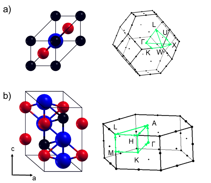
In this work, we consider the two trialkali antimonides with chemical formulas and . According to the pioneering experimental study performed by McCarroll [58], the former compound is more stable than the latter, which, however, can be formed as an alloy of the type upon a proper combination of the constituting atoms. has a face-centered cubic (FCC) Bravais lattice with the Sb atom located at the origin , while the alkali atoms are found at (K) and (Na) positions. has a hexagonal crystal structure with 8 atoms in the unit cell [58]. To model this structure we adopt the experimentally proposed lattice with two Na atoms at , four K atoms at and , and two Sb atoms at . Starting from the experimental crystal structures [58], a volume optimization based on the Birch-Murnaghan fit [59, 60] is performed. The two structures are depicted in Fig. 1, where also the corresponding Brillouin zones and the high-symmetry points in the conventional notation proposed in Ref. [61] are shown. The lattice parameter obtained for is Å, which is 0.02 Å larger than the experimental one [58]. For the hexagonal structure of , we obtain an in-plane lattice parameter Å and an out-of-plane lattice vector Å. Both values are 0.03 Å smaller compared to the measurements, which, however, were performed on a non perfectly stoichiometric structure [58]. The ratio equal to 1.95 is in excellent agreement with the experimental reference [58].
The interatomic distances obtained in both compounds are in overall agreement with the experimental values [58]. We notice that the Na-Sb spacing increases from 3.22 Å to 3.35 Å from the cubic to the hexagonal phase. Also the K-Sb distance is subject to a similar behavior being 3.87 Å in and 3.63 Å as well as 3.70 Å in , where two types of K-Sb coordination exist. Very different trends are instead obtained for the Na-Na and the K-K distances, which are more crucially affected by the crystal structure. The former is 5.58 Å in and 3.87 Å in , while, conversely, the latter is 3.63 Å in the hexagonal phase and 5.47 Å in the cubic one. Finally, the Na-K distance is larger in (3.70 Å) than in (3.35 Å).
III.2 Electronic structure
In the next step of our investigation, we focus on the electronic structure of the materials. Both Na2KSb and NaK2Sb, are characterized by a direct band gap at (see Fig. 2). As expected, the results provided by DFT with the semi-local PBE functional (Fig. 2, black curves) severely underestimate the size of the gap compared to (magenta diamonds). The inclusion of the QP correction leads to a band-gap of 1.51 eV in Na2KSb (Fig. 2, left) and of 0.96 eV in NaK2Sb (Fig. 2, right). Both values are more than twice as large as those yielded by DFT (0.70 eV in Na2KSb and 0.44 eV in NaK2Sb). An early theoretical work based on the localized spherical wave method predicted for Na2KSb a gap of the order of 1 eV [24].

By aligning the DFT and band structures at the VBM, we are able to appreciate the overall effect of the QP correction in the valence and conduction regions (see Fig. 2). In the case of Na2KSb, the occupied states that are closest to the gap are identically reproduced by DFT and . On the other hand, in the valence region of the band-structure of NaK2Sb we notice a lowering by approximately 100 meV of the occupied band around -1.5 eV, when the self-energy contribution is accounted for (see Fig. 2, right). This finding highlights the importance of performing a calculation to solve the QP equation for all the electronic states of interest. In the conduction region of both materials, the QP correction exerts an almost rigid shift to the bands. No significant variations affect the band curvatures and the effective masses.
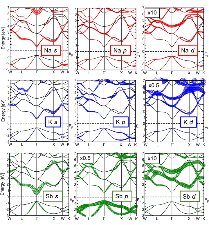
Further insight about the electronic properties can be gained by inspecting the orbital-projected character of the band structure (see Fig. 3 for cubic Na2KSb and Fig. 4 for hexagonal NaK2Sb). This analysis is relevant from many different perspectives: First, understanding the nature of the electronic states in the valence and conduction region provides the key ingredients to interpret and predict the optical absorption of the material. Second, the non-stoichimetric compositions and/or the polycrystalline nature often exhibited by multi-alkali antimonide samples [4] demand reliable theoretical references to identify specific structures or crystalline phases, for example, via x-ray spectroscopy [31]. For this purpose, the knowledge of the atomic and orbital character of the bands is essential for the interpretations of the corresponding experiments [62, 63, 64]. Finally, gaining information about the atomic and orbital character of the wave-functions is also essential in view of engineering multi-alkali antimonides compositions and alloys with enhanced performance in photocathode applications.
In both considered systems, the valence band is dominated by Sb -states which are subject to a spin-orbit splitting of a few hundreds meV at the high-symmetry points in the Brillouin zone (see Fig. 7 and related discussion in the Appendix). This leads to an overall reduction in the band-gap on the order of 0.2 eV. These findings are in agreement with previous results obtained on the same materials [28] as well as on related compounds [29, 65]. In the hexagonal phase, additional contributions from both Na and K -orbitals, as far as the higher and flatter bands are concerned, and by -states from Sb and Na in lower-energies and more dispersive bands. The conduction band minimum (CBm), at the bottom of a parabolic band, has a marked -like character in both materials, with dominant contributions from Sb and, to a minor extent, also to K and Na. A careful inspection of the band structure of cubic Na2KSb (Fig. 3) reveals that the minimum at X, which belongs to a different band than the CBm, has a hybridized character involving mainly Na -states as well as Sb and K -states. Higher-energy bands include also contributions from -states of all the involved species, as well as K -states (see Fig. 3).
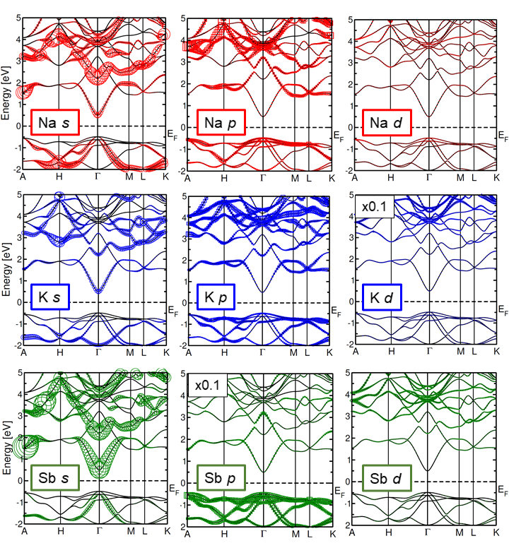
The scenario is more faceted in the case of the hexagonal crystal NaK2Sb. In the corresponding conduction region, bands directly above the CBm bear mainly Sb and -like contributions (see Fig. 4). Higher-energy bands in the cubic phase are dominated by K -states. In hexagonal NaK2Sb, on the other hand, hybridized -orbitals of the alkali atoms (Na and K) mainly contribute to the conduction bands above the CBm (see Fig. 4). The differences in the unoccupied states of the two examined materials offers promising perspectives to use x-ray absorption spectroscopy to identify their fingerprints [66] in polycrystalline samples, where the two structures can coexist.
III.3 Optical properties
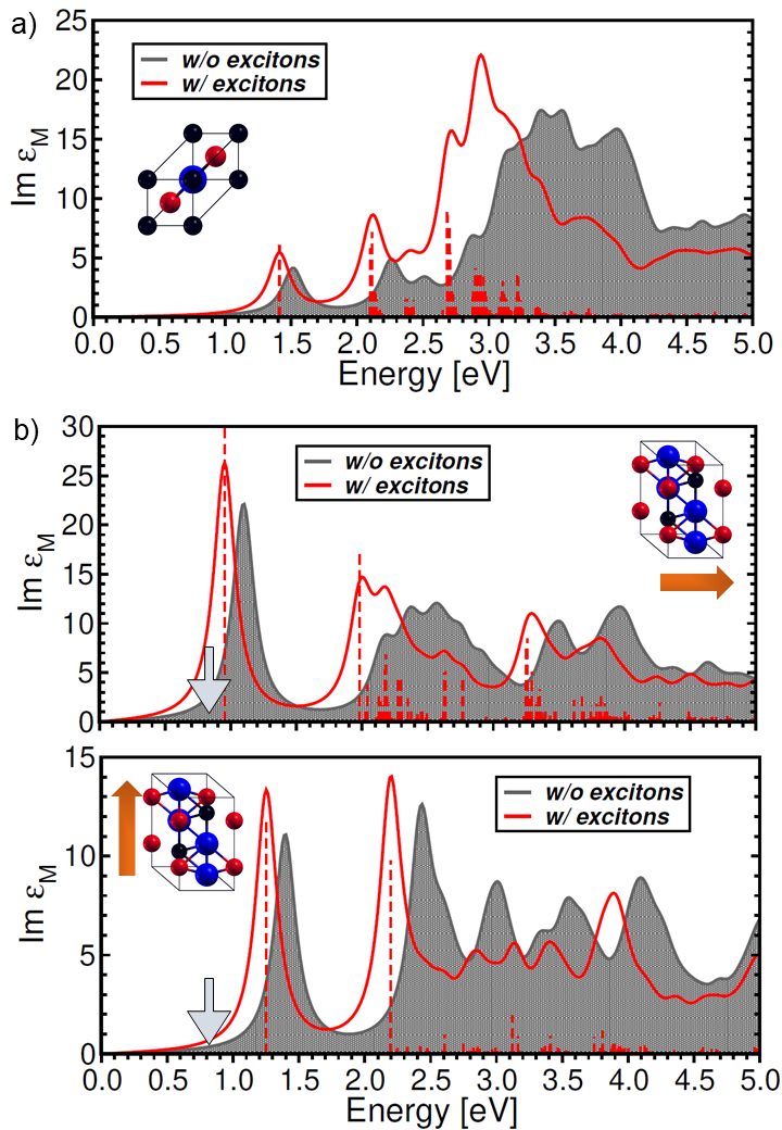
The electronic structure discussed above is the cornerstone to interpret the imaginary parts of the dielectric functions calculated for the two materials (see Fig. 5). This quantity provides information about the optical absorption of the systems. In both Na2KSb and in NaK2Sb, the first bright excitation is found at the boundary between the visible and the infrared region. In the case of cubic Na2KSb (Fig. 5a), where the dielectric function is fully defined by one diagonal component, the first maximum corresponding to the first excited state appears at 1.41 eV. This peak is formed by one single excitation, which is triple-degenerate for symmetry reasons, and has a binding energy of 100 meV. The latter quantity is estimated as the difference between the peak energy in the BSE spectrum and the QP gap, which also coincides with the energy of the first peak in the spectrum computed without excitons (independent QP approximation, IQPA, shown in Fig. 5a). In spite of its peaked shape, the first maximum in Fig. 5a) is not excitonic in nature, as it is present in the same form and with almost unaltered strength also in the IQPA spectrum (shaded grey area). From the analysis of the BSE eigenvectors, computed from Eq. 1, we find that this excitation corresponds to the vertical transition at between the Sb -like VBM and the Sb -like CBm. Above the first maximum, a second peak is found at 2 eV, followed by additional ones between 2.5 and 3.5 eV. These higher-energy excitations experience a more considerable redistribution of the oscillator strength compared to the first one, which is ascribed to excitonic effects. Our results are in excellent agreement with the available experimental reference [67], where the maximum at 3 eV is particularly evident but also the absorption onset at about 1.5 eV and a shoulder close to 2 eV appears.
The dielectric function of hexagonal NaK2Sb is given by two independent components, corresponding to the in-plane and the out-of-plane response of the material (see Fig. 5b and insets). Both components are characterized by an intense peak at lowest-energy, namely at 0.95 eV and 1.25 eV in the in-plane and in the out-of-plane direction, respectively. In both cases, an optically silent excitation is present at lowest energy (0.82 eV), stemming from the transition at between the first and second uppermost valence bands and the CBm (see Fig. 6, left panel). These valence states are those where the Na and K -character is maximized (Fig. 4): the transition probability to the Sb -like CBm is reasonably minimized. Similar to the cubic phase and in spite of their sharp character, also in hexagonal NaK2Sb, the first peaks are not excitonic, as a maximum of comparable intensity is found also in the corresponding IQPA spectra (see Fig. 5b). Due to the presence of a dark excitation at lowest energy, we adopt in this case an alternative and more appropriate definition of the exciton binding energy, given by the difference between the first maxima in the BSE and in the IQPA. This definition is best applied to organic systems, where single-particle excitations are well distinguished from one another [62, 68, 69], as well as in composite systems, such as hybrid systems [70, 64, 71] and heterostructures [72, 73, 74]. The binding energy associated to the lowest-energy peaks in the in-plane and out-of-plane optical components of NaK2Sb is 150 meV. Also the bright excitations at the two onsets stem from vertical transitions targeting the CBm at . The first bright excitation in the in-plane component of the spectrum, which is also double degenerate for symmetry reasons (one BSE solution is along the -axis and the other one along ), comes from the third and fourth highest occupied bands (Fig. 6, middle panel), which have a predominant Sb -nature (see Fig. 4). Finally, first maximum in the out-of-plane component, is generated by a non-degenerate excitation from the parabolic valence band with Sb -character to the Sb -like CBm (see Fig. 6, right panel, and Fig. 4).
The higher-energy maxima in both components of the optical spectra of NaK2Sb appear in the middle of the visible band, around 2 eV. Interestingly, in the out-of-plane component, another sharp peak appears at 2.2 eV, again with a clear counterpart in the IQPA spectrum approximately 200 meV above it, which remarks its non-excitonic character. Additional peaks are distinguishable at higher energies. Compared to the cubic material discussed above, in hexagonal NaK2Sb, a redistribution of the oscillator strength to lower energies is still visible by comparing results of calculations with and without excitonic effects. However, in this case, they mainly result in a rigid red-shift of the peaks.
IV Summary and Conclusions
In summary, we have presented an ab initio many-body study of the electronic and optical properties of Na2KSb and NaK2Sb, two members of the multi-alkali antimonide family of materials, which are regarded with interest for applications as vacuum electron sources. Both materials exhibit a direct band gap at , which is on the order of 1.5 eV in Na2KSb and 1.0 eV in NaK2Sb. Spin-orbit coupling induces a reduction of the gap by approximately 200 meV in both systems. The valence region is dominated by Sb -states while the lowest conduction band has a pronounced parabolic dispersion due to the Sb orbital partially hybridized with the -states of the alkali species too. Higher-energy unoccupied bands receive contributions from the -electrons of all the atoms, with a predominance from potassium. While these main characteristics are common to both crystals, fine details in the orbital hybridization in the conduction region, suggests the use of x-ray absorption spectroscopy to identify the two compounds in polycrystalline samples.
The imaginary part of the dielectric functions of both Na2KSb and NaK2Sb are characterized by maxima at the boundary between the visible and the infrared region. The lowest-energy excitation in cubic Na2KSb appears at 1.41 eV, approximately 0.5 eV higher in energy compared to the first bright peak in the dielectric function of NaK2Sb. In this material, a dark excitation is found at lowest energy (0.82 eV). In both materials, excitonic effects are marginal and mainly consist of a red-shift of the spectral weight towards lower energies. Binding energies of the order of 100 meV are found for all the considered excitons. Interestingly, the lowest-energy excitations are single-particle in nature, in spite of their relatively large oscillator strength and their sharply peaked shape.
In conclusion, the electronic and optical properties computed for Na2KSb and NaK2Sb at the level of all-electron DFT and MBPT reveal desirable characteristics for the use of these materials as next-generation vacuum electron sources. The absorption threshold of both materials around 1 – 1.5 eV as well as the relatively weak binding strength of the lowest-energy excitations are particularly promising in view of photoemission in the infrared region. The examined Na-based alkali antimonides exhibit similar electronic and optical properties as their Cs-based counterparts obtained within the same methodological framework [30, 31]. This finding hints that the replacement of the heavier Cs atom with the lighter Na does not affect the favorable photoemission characteristics of multi-alkali antimonides. Even more importantly, this result suggests the potential for fine-tuning the electronic properties of these materials via tailored compositions and alloys.
Data availability statement
The data that support the findings of this study are available upon reasonable request from the authors.
Acknowledgements.
The authors are grateful to Thorsten Kamps, Julius Kühn, Sonal Mistry, and Martin Schmeißer, for stimulating discussions. This work is partly funded by the German Federal Ministry of Education and Research (Professorinnenprogramm III) as well as from the Lower Saxony State (Professorinnen für Niedersachsen).Appendix: Effects of spin-orbit coupling on DFT
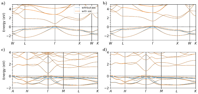
In Fig. 7 we report the results of DFT calculations performed on Na2KSb and NaK2Sb including spin-orbit coupling. For this purpose, we used the all-electron, full potential code FHI-aims [75] with the intermediate default settings for the basis-set and the integration grids. For Na2KSb and NaK2Sb, a 181818 and a 12126 k-meshes are used to sample the Brillouin zone. The effect of spin-orbit coupling is accounted for based on a non-self-consistent post-self-consistent-field approximation [76]. For these calculations, we employ both PBE as well as the SCAN functional [77], implementing the meta-generalized-gradient-approximation, which was recently established to offer an optimal trade-off between accuracy and numerical costs for the evaluation of the band-gaps of Cs-based alkali-antimonides and tellurides [65].
The impact of spin-orbit coupling is visible only in the valence region and in the vicinity of the high-symmetry points where bands are split (see Fig. 7). In Na2KSb, the magnitude of the band splitting ranges from 0.25 eV at the -point up to about 0.55 eV at . No spitting occurs at the -point. In NaK2Sb, spin-orbit coupling splits the bands at all high-symmetry points, ranging from 0.15 eV at to 0.30 eV at . In both materials, the valence band maximum is shifted upwards at , thereby reducing the band gap by about 0.2 eV.
Comparing now the effect of the xc functional, we notice that the most striking difference is the rigid shift of the conduction bands, which results in an increased band gap in both materials. Using the SCAN functional we obtain a band gap of 1.32 eV and 0.86 eV for Na2KSb and NaK2Sb respectively. These values are quite close to those calculated from on top of PBE, in agreement with the results obtained for Cs3Sb at the same level of theory [65].
References
- Hernandez-Garcia et al. [2008] C. Hernandez-Garcia, P. G. O Shea, and M. L. Stutzman, Electron sources for accelerators, Phys. Today 61, 44 (2008).
- Dowell et al. [2010] D. Dowell, I. Bazarov, B. Dunham, K. Harkay, C. Hernandez-Garcia, R. Legg, H. Padmore, T. Rao, J. Smedley, and W. Wan, Cathode r&d for future light sources, Nucl. Instrum. Methods Phys. Res. A 622, 685 (2010).
- Musumeci et al. [2018] P. Musumeci, J. G. Navarro, J. Rosenzweig, L. Cultrera, I. Bazarov, J. Maxson, S. Karkare, and H. Padmore, Advances in bright electron sources, Nucl. Instrum. Methods Phys. Res. A 907, 209 (2018).
- Schmeißer et al. [2018] M. A. Schmeißer, S. Mistry, H. Kirschner, S. Schubert, A. Jankowiak, T. Kamps, and J. Kühn, Towards the operation of cs-k-sb photocathodes in superconducting rf photoinjectors, Phys. Rev. Accel. Beams 21, 113401 (2018).
- Dunham et al. [2013] B. Dunham, J. Barley, A. Bartnik, I. Bazarov, L. Cultrera, J. Dobbins, G. Hoffstaetter, B. Johnson, R. Kaplan, S. Karkare, V. Kostroun, Y. Li, M. Liepe, X. Liu, F. Loehl, J. Maxson, P. Quigley, J. Reilly, D. Rice, D. Sabol, E. Smith, K. Smolenski, M. Tigner, V. Vesherevich, D. Widger, and Z. Zhao, Record high-average current from a high-brightness photoinjector, Appl. Phys. Lett. 102, 034105 (2013).
- Michelato et al. [1994] P. Michelato, P. Gallina, and C. Pagani, Alkali photocathode development for superconducting rf guns, Nucl. Instrum. Methods Phys. Res. A 340, 176 (1994).
- Di Bona et al. [1997] A. Di Bona, F. Sabary, S. Joly, P. Michelato, D. Sertore, C. Pagani, and S. Valeri, Development, operation and analysis of bialkali antimonide photocathodes for high-brightness photo-injectors, Nucl. Instrum. Methods Phys. Res. A 385, 385 (1997).
- Smedley et al. [2009] J. Smedley, T. Rao, and E. Wang, K2cssb cathode development, AIP Conf. Proc. 1149, 1062 (2009).
- Cultrera et al. [2011] L. Cultrera, I. Bazarov, A. Bartnik, B. Dunham, S. Karkare, R. Merluzzi, and M. Nichols, Thermal emittance and response time of a cesium antimonide photocathode, Appl. Phys. Lett. 99, 152110 (2011).
- Vecchione et al. [2011] T. Vecchione, I. Ben-Zvi, D. Dowell, J. Feng, T. Rao, J. Smedley, W. Wan, and H. Padmore, A low emittance and high efficiency visible light photocathode for high brightness accelerator-based x-ray light sources, Appl. Phys. Lett. 99, 034103 (2011).
- Schubert et al. [2013] S. Schubert, M. Ruiz-Osés, I. Ben-Zvi, T. Kamps, X. Liang, E. Muller, K. Müller, H. Padmore, T. Rao, X. Tong, T. Vecchione, and J. Smedley, Bi-alkali antimonide photocathodes for high brightness accelerators, APL Mater. 1, 032119 (2013).
- Mammei et al. [2013] R. Mammei, R. Suleiman, J. Feingold, P. Adderley, J. Clark, S. Covert, J. Grames, J. Hansknecht, D. Machie, M. Poelker, T. Rao, J. Smedley, J. Walsh, J. L. McCarter, and M. Ruiz-Oses, Charge lifetime measurements at high average current using a k 2 cssb photocathode inside a dc high voltage photogun, Phys. Rev. Accel. Beams 16, 033401 (2013).
- Ruiz-Osés et al. [2014] M. Ruiz-Osés, S. Schubert, K. Attenkofer, I. Ben-Zvi, X. Liang, E. Muller, H. Padmore, T. Rao, T. Vecchione, J. Wong, J. Xie, and J. Smedley, Direct observation of bi-alkali antimonide photocathodes growth via in operando x-ray diffraction studies, APL Mater. 2, 121101 (2014).
- Cultrera et al. [2015] L. Cultrera, S. Karkare, H. Lee, X. Liu, I. Bazarov, and B. Dunham, Cold electron beams from cryocooled, alkali antimonide photocathodes, Phys. Rev. Accel. Beams 18, 113401 (2015).
- Xie et al. [2016] H. Xie, I. Ben-Zvi, T. Rao, T. Xin, and E. Wang, Experimental measurements and theoretical model of the cryogenic performance of bialkali photocathode and characterization with monte carlo simulation, Phys. Rev. Accel. Beams 19, 103401 (2016).
- Orlov et al. [2004] D. Orlov, U. Weigel, D. Schwalm, A. Terekhov, and A. Wolf, Ultra-cold electron source with a gaas-photocathode, Nucl. Instrum. Methods Phys. Res. A 532, 418 (2004).
- Sinclair et al. [2007] C. Sinclair, P. Adderley, B. Dunham, J. Hansknecht, P. Hartmann, M. Poelker, J. Price, P. Rutt, W. Schneider, and M. Steigerwald, Development of a high average current polarized electron source with long cathode operational lifetime, Phys. Rev. Accel. Beams 10, 023501 (2007).
- Kuriki et al. [2011] M. Kuriki, C. Shonaka, H. Iijima, D. Kubo, H. Okamoto, H. Higaki, K. Ito, M. Yamamoto, T. Konomi, S. Okumi, M. Kuwahara, and T. Nakanishi, Dark-lifetime degradation of gaas photo-cathode at higher temperature, Nucl. Instrum. Methods Phys. Res. A 637, S87 (2011).
- [19] J. Maxson, L. Cultrera, C. Gulliford, and I. Bazarov, Measurement of the tradeoff between intrinsic emittance and quantum efficiency from a naksb photocathode near threshold, Appl. Phys. Lett. .
- Ding et al. [2017] Z. Ding, M. Gaowei, J. Sinsheimer, J. Xie, S. Schubert, H. Padmore, E. Muller, and J. Smedley, In-situ synchrotron x-ray characterization of k2cssb photocathode grown by ternary co-evaporation, J. Appl. Phys. 121, 055305 (2017).
- Panuganti et al. [2021] H. Panuganti, E. Chevallay, V. Fedosseev, and M. Himmerlich, Synthesis, surface chemical analysis, lifetime studies and degradation mechanisms of cs-k-sb photocathodes, Nucl. Instrum. Methods Phys. Res. A 986, 164724 (2021).
- Erjavec [2001] B. Erjavec, Vacuum problems of miniaturization of vacuum electronic components: a new generation of compact photomultipliers, Vacuum 64, 15 (2001).
- Cultrera et al. [2016a] L. Cultrera, H. Lee, and I. Bazarov, Alkali antimonides photocathodes growth using pure metals evaporation from effusion cells, J. Vac. Sci. Technol. B 34, 011202 (2016a).
- Ettema and de Groot [2000] A. Ettema and R. de Groot, Electronic structure of na 3 sb and na 2 ksb, Phys. Rev. B 61, 10035 (2000).
- Ettema and de Groot [2002] A. Ettema and R. de Groot, Electronic structure of cs 2 ksb and k 2 cssb, Phys. Rev. B 66, 115102 (2002).
- Kalarasse et al. [2010a] L. Kalarasse, B. Bennecer, and F. Kalarasse, Optical properties of the alkali antimonide semiconductors cs3sb, cs2ksb, csk2sb and k3sb, J. Phys. Chem. Solids 71, 314 (2010a).
- Kalarasse et al. [2010b] L. Kalarasse, B. Bennecer, F. Kalarasse, and S. Djeroud, Pressure effect on the electronic and optical properties of the alkali antimonide semiconductors cs3sb, kcs2sb, csk2sb and k3sb: Ab initio study, J. Phys. Chem. Solids 71, 1732 (2010b).
- Yalameha et al. [2018] S. Yalameha, Z. Nourbakhsh, and A. Vaez, Hydrostatic strain-induced topological phase of kna2sb, 468, 279 (2018).
- [29] Z. Khan, G. Murtaza, A. A. Khan, A. Laref, N. A. Kattan, and M. Haneef, Different physical properties of bi-alkali pnictogen compounds using density functional theory, Int. J. Energy Res. https://doi.org/10.1002/er.6351.
- Cocchi et al. [2018] C. Cocchi, S. Mistry, M. Schmeißer, J. Kühn, and T. Kamps, First-principles many-body study of the electronic and optical properties of csk2sb, a semiconducting material for ultra-bright electron sources, J. Phys. Condens. Matter. 31, 014002 (2018).
- [31] C. Cocchi, S. Mistry, M. Schmeißer, R. Amador, J. Kühn, and T. Kamps, Electronic structure and core electron fingerprints of caesium-based multi-alkali antimonides for ultra-bright electron sources, Sci. Rep. .
- Berglund and Spicer [1964] C. N. Berglund and W. E. Spicer, Photoemission studies of copper and silver: theory, Phys. Rev. 136, A1030 (1964).
- Antoniuk et al. [2020] E. R. Antoniuk, Y. Yue, Y. Zhou, P. Schindler, W. A. Schroeder, B. Dunham, P. Pianetta, T. Vecchione, and E. J. Reed, Generalizable density functional theory based photoemission model for the accelerated development of photocathodes and other photoemissive devices, Phys. Rev. B 101, 235447 (2020).
- Bazarov et al. [2011] I. Bazarov, L. Cultrera, A. Bartnik, B. Dunham, S. Karkare, Y. Li, X. Liu, J. Maxson, and W. Roussel, Thermal emittance measurements of a cesium potassium antimonide photocathode, Appl. Phys. Lett. 98, 224101 (2011).
- Natarajan et al. [2001] A. Natarajan, A. Kalghatgi, B. Bhat, and M. Satyam, Role of the cesium antimonide layer in the na 2 ksb/cs 3 sb photocathode, J. Appl. Phys. 90, 6434 (2001).
- Cultrera et al. [2013] L. Cultrera, S. Karkare, B. Lillard, A. Bartnik, I. Bazarov, B. Dunham, W. Schaff, and K. Smolenski, Growth and characterization of rugged sodium potassium antimonide photocathodes for high brilliance photoinjector, Appl. Phys. Lett. 103, 103504 (2013).
- Cultrera et al. [2016b] L. Cultrera, C. Gulliford, A. Bartnik, H. Lee, and I. Bazarov, Ultra low emittance electron beams from multi-alkali antimonide photocathode operated with infrared light, Appl. Phys. Lett. 108, 134105 (2016b).
- Chikawa et al. [1961] J.-i. Chikawa, S. Imamura, K. Tanaka, and M. Shiojiri, Crystal structures and electrical properties of alkali antimonides, J. Phys. Soc. Jpn. 16, 1175 (1961).
- [39] D. Fisher, A. McDonie, and A. Sommer, Band-bending effects in na2ksb and k2cssb photocathodes, J. Appl. Phys. .
- Dolizy et al. [1988] P. Dolizy, F. Groliere, and M. Lemonier, High performance with trialkaline antimonide photocathodes, in Advances in Electronics and Electron Physics, Vol. 74 (Elsevier, 1988) pp. 331–338.
- Hohenberg and Kohn [1964] P. Hohenberg and W. Kohn, Inhomogeneus electron gas, Phys. Rev. 136, B864 (1964).
- Onida et al. [2002] G. Onida, L. Reining, and A. Rubio, Electronic excitations: density-functional versus many-body green’s-function approaches, Rev. Mod. Phys. 74, 601 (2002).
- Kohn and Sham [1965] W. Kohn and L. J. Sham, Self-consistent equations including exchange and correlation effects, Phys. Rev. 140, A1133 (1965).
- Hedin [1965] L. Hedin, New method for calculating the one-particle green’s function with application to the electron gas problem, Phys. Rev. 139, A796 (1965).
- Hybertsen and Louie [1985] M. S. Hybertsen and S. G. Louie, First-principles theory of quasiparticles: Calculation of band gaps in semiconductor and insulators, Phys. Rev. Lett. 55, 1418 (1985).
- Salpeter and Bethe [1951] E. E. Salpeter and H. A. Bethe, A relativistic equation for bound-state problems, Phys. Rev. 84, 1232 (1951).
- Vorwerk et al. [2019] C. Vorwerk, B. Aurich, C. Cocchi, and C. Draxl, Bethe–salpeter equation for absorption and scattering spectroscopy: implementation in the exciting code, Electron. Struct. 1, 037001 (2019).
- Fox [2001] M. Fox, Optical properties of solids (2001).
- Yeh [1980] P. Yeh, Optics of anisotropic layered media: a new 4 4 matrix algebra, Surf. Sci. 96, 41 (1980).
- Puschnig and Ambrosch-Draxl [2006] P. Puschnig and C. Ambrosch-Draxl, Atomistic modeling of optical properties of thin films, Adv. Energy Mater. 8, 1151 (2006).
- Vorwerk et al. [2016] C. Vorwerk, C. Cocchi, and C. Draxl, Layeroptics: Microscopic modeling of optical coefficients in layered materials, Comput. Phys. Commun. 201, 119 (2016).
- Passler and Paarmann [2017] N. C. Passler and A. Paarmann, Generalized 4 4 matrix formalism for light propagation in anisotropic stratified media: study of surface phonon polaritons in polar dielectric heterostructures, JOSA B 34, 2128 (2017).
- Gulans et al. [2014] A. Gulans, S. Kontur, C. Meisenbichler, D. Nabok, P. Pavone, S. Rigamonti, S. Sagmeister, U. Werner, and C. Draxl, exciting: a full-potential all-electron package implementing density-functional theory and many-body perturbation theory, J. Phys. Condens. Matter. 26, 363202 (2014).
- Vorwerk et al. [2017] C. Vorwerk, C. Cocchi, and C. Draxl, Addressing electron-hole correlation in core excitations of solids: An all-electron many-body approach from first principles, Phys. Rev. B 95, 155121 (2017).
- Perdew et al. [1996] J. P. Perdew, K. Burke, and M. Ernzerhof, Generalized gradient approximation made simple, Phys. Rev. Lett. 77, 3865 (1996).
- Nabok et al. [2016] D. Nabok, A. Gulans, and C. Draxl, Accurate all-electron g 0 w 0 quasiparticle energies employing the full-potential augmented plane-wave method, Phys. Rev. B 94, 035118 (2016).
- Kokalj [1999] A. Kokalj, Xcrysden—a new program for displaying crystalline structures and electron densities, J. Mol. Graphics Modelling 17, 176 (1999).
- McCarroll [1960] W. McCarroll, Phases in the photoelectric sodium-potassium-antimony system, J. Phys. Chem. Solids 16, 30 (1960).
- Birch [1947] F. Birch, Finite elastic strain of cubic crystals, Phys. Rev. 71, 809 (1947).
- Murnaghan [1944] F. Murnaghan, The compressibility of media under extreme pressures, Proc. Natl. Acad. Sci. USA 30, 244 (1944).
- Setyawan and Curtarolo [2010] W. Setyawan and S. Curtarolo, High-throughput electronic band structure calculations: Challenges and tools, Comp. Mater. Sci. 49, 299 (2010).
- Cocchi and Draxl [2015] C. Cocchi and C. Draxl, Bound excitons and many-body effects in x-ray absorption spectra of azobenzene-functionalized self-assembled monolayers, Phys. Rev. B 92, 205105 (2015).
- Cocchi et al. [2016] C. Cocchi, H. Zschiesche, D. Nabok, A. Mogilatenko, M. Albrecht, Z. Galazka, H. Kirmse, C. Draxl, and C. T. Koch, Atomic signatures of local environment from core-level spectroscopy in - ga 2 o 3, Phys. Rev. B 94, 075147 (2016).
- Vorwerk et al. [2018] C. Vorwerk, C. Hartmann, C. Cocchi, G. Sadoughi, S. N. Habisreutinger, R. Félix, R. G. Wilks, H. J. Snaith, M. Bär, and C. Draxl, Exciton-dominated core-level absorption spectra of hybrid organic-inorganic lead halide perovskites, J. Phys. Chem. Lett. 9, 1852 (2018).
- Sassnick and Cocchi [2021] H.-D. Sassnick and C. Cocchi, Electronic structure of cesium-based photocathode materials from density functional theory: Performance of pbe, scan, and hse06 functionals, Electronic Structure 10.1088/2516-1075/abfb08 (2021).
- Cocchi [2020] C. Cocchi, X-ray absorption fingerprints from cs atoms in cs3sb, Phys. Status Solidi (RRL) 14, 2000194 (2020).
- Ebina and Takahashi [1973] A. Ebina and T. Takahashi, Transmittance spectra and optical constants of alkali-antimony compounds k 3 sb, na 3 sb, and na 2 ksb, Phys. Rev. B 7, 4712 (1973).
- Cocchi and Draxl [2017] C. Cocchi and C. Draxl, Understanding the effects of packing and chemical terminations on the optical excitations of azobenzene-functionalized self-assembled monolayers, J. Phys. Condens. Matter. 29, 394005 (2017).
- Beyer et al. [2019] P. Beyer, D. Pham, C. Peter, N. Koch, E. Meister, W. Brütting, L. Grubert, S. Hecht, D. Nabok, C. Cocchi, C. Draxl, and A. Opitz, State-of-matter-dependent charge-transfer interactions between planar molecules for doping applications, Chem. Mater. 31, 1237 (2019).
- Fu et al. [2017] Q. Fu, C. Cocchi, D. Nabok, A. Gulans, and C. Draxl, Graphene-modulated photo-absorption in adsorbed azobenzene monolayers, Phys. Chem. Chem. Phys. 19, 6196 (2017).
- Turkina et al. [2019] O. Turkina, D. Nabok, A. Gulans, C. Cocchi, and C. Draxl, Hybrid materials: Electronic and optical excitations at the pyridine/ZnO (100) hybrid interface, Adv. Theory Simul. 2, 1800108 (2019).
- Aggoune et al. [2017] W. Aggoune, C. Cocchi, D. Nabok, K. Rezouali, M. Akli Belkhir, and C. Draxl, Enhanced light–matter interaction in graphene/h-bn van der waals heterostructures, J. Phys. Chem. Lett. 8, 1464 (2017).
- Lau et al. [2019] K. W. Lau, C. Cocchi, and C. Draxl, Electronic and optical excitations of two-dimensional zrs 2 and hfs 2 and their heterostructure, Phys. Rev. Materials 3, 074001 (2019).
- Aggoune et al. [2020] W. Aggoune, C. Cocchi, D. Nabok, K. Rezouali, M. A. Belkhir, and C. Draxl, Structural, electronic, and optical properties of periodic graphene/h-bn van der waals heterostructures, Phys. Rev. Materials 4, 084001 (2020).
- Blum et al. [2009] V. Blum, R. Gehrke, F. Hanke, P. Havu, V. Havu, X. Ren, K. Reuter, and M. Scheffler, Ab initio molecular simulations with numeric atom-centered orbitals, Comput. Phys. Commun. 180, 2175 (2009).
- Huhn and Blum [2017] W. P. Huhn and V. Blum, One-hundred-three compound band-structure benchmark of post-self-consistent spin-orbit coupling treatments in density functional theory, Phys. Rev. Materials 1, 033803 (2017).
- Sun et al. [2015] J. Sun, A. Ruzsinszky, and J. P. Perdew, Strongly constrained and appropriately normed semilocal density functional, Phys. Rev. Lett. 115, 036402 (2015).