Intense optical parametric amplification in dispersion-engineered nanophotonic lithium niobate waveguides
Abstract
Strong amplification in integrated photonics is one of the most desired optical functionalities for computing, communications, sensing, and quantum information processing. Semiconductor gain and cubic nonlinearities, such as four-wave mixing and stimulated Raman and Brillouin scattering, have been among the most studied amplification mechanisms on chip. Alternatively, material platforms with strong quadratic nonlinearities promise numerous advantages with respect to gain and bandwidth, among which nanophotonic lithium niobate is one of the most promising candidates. Here, we combine quasi-phase matching with dispersion engineering in nanophotonic lithium niobate waveguides and achieve intense optical parametric amplification. We measure a broadband phase-sensitive on-chip amplification larger than 50 dB/cm in a 6-mm-long waveguide. We further confirm high gain operation in the degenerate and non-degenerate regimes by amplifying vacuum fluctuations to macroscopic levels, with on-chip gains exceeding 100 dB/cm over 600 nm of bandwidth around 2 m. Our results unlock new possibilities for on-chip few-cycle nonlinear optics, mid-infrared photonics, and quantum photonics.
1 Introduction
Amplification is an important element of a wide range of optical systems, from computing [1] and sensing [2] to quantum information processing [3] and communications [4]. In integrated photonics, achieving intense amplification remains an important challenge. In silicon-based platforms, significant attention has been focused on cubic nonlinearities to realize amplification through four-wave mixing (FWM) [5, 6], stimulated Raman scattering (SRS) [7], and stimulated Brillouin scattering (SBS) [8]. Despite recent promising advances, the weak nature of these nonlinearities and the adverse effects of other competing nonlinearities hamper the amount of gain and bandwidths associated with these mechanisms. Another option providing gain on integrated platforms is the semiconductor optical amplifier (SOA). SOAs have evolved in the past decades as one of the leading optical gain mechanisms [9, 10], and heterogeneous integration of III-V SOAs with other platforms, especially silicon, has been one of the most active research directions in integrated photonics [10]. However, their limited bandwidth and integration challenges hinder their utilization in several applications, such as those that require accessing gain in multiple places on a chip. Furthermore, semiconductor gain is not phase-sensitive, limiting its use in quantum and communication applications that require noiseless amplification, e.g. processing of quantum microcombs [11] and few-cycle squeezed vacuum [12]. Hence, an integrated platform with a native gain mechanism that enables intense and phase-sensitive optical amplification of ultra-short pulses can address several of the current challenges in photonics.
Quadratic nonlinearities provide an alternative path for achieving strong optical amplification through three-wave mixing [13, 14]. Such processes have been extensively used in bulk optical systems leading to amplification at wavelengths where other gain mechanisms are not easily available [15, 16]. Recently, integrated photonic platforms with strong quadratic nonlinearities have attracted significant attention since they can provide a range of functionalities unavailable in other platforms [17, 18, 19, 20]. Examples of these processes include second harmonic and supercontinuum generation [21, 22], electro-optic modulation [23, 24], quadratic parametric oscillators [25, 26], and bright sources of entangled photons [27]. Despite the recent significant progress, realization of intense optical amplification in quadratically nonlinear integrated photonics has remained elusive.
In integrated photonics, strong quadratic nonlinear interactions have been enabled by tight spatial confinement of the waveguide modes and the possibility to provide momentum conservation through modal [28] or quasi-phase matching [21, 22]. Further enhancement has also been achieved by utilization of appropriate resonators [25, 26], however, resonant dynamics associated with the cavity lifetime are typically not appropriate for amplification in many applications as they limit the gain bandwidth.
In this work, we present an integrated, high-gain, broadband, traveling-wave, optical parametric amplifier based on quadratic nonlinearities. We show phase-sensitive amplification by operating the amplifier at degeneracy. The large parametric gain of our device is enough to amplify quantum fluctuations to macroscopic levels, therefore allowing the amplifier to function as an optical parametric generator of infrared radiation. Our design strategy is based on quasi-phase matching combined with spatio-temporal confinement of pulses in dispersion-engineered lithium niobate waveguides; a combination that is not easily available on other nonlinear photonic platforms.
2 Device Design and Fabrication
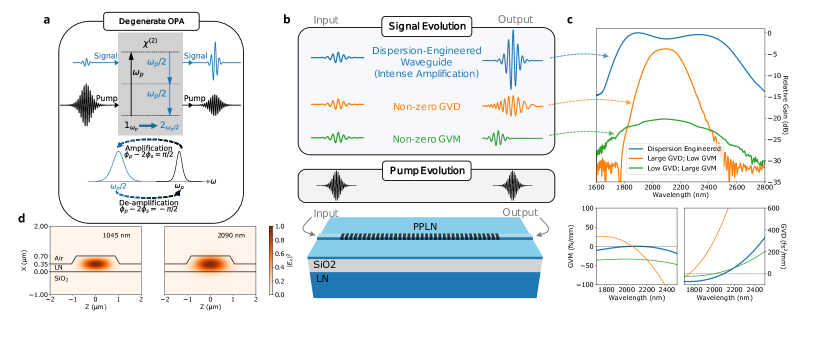
We focus on optical parametric amplification (OPA) at degeneracy through three-wave mixing in a waveguide (Fig. 1a). As shown in Fig. 1b, for efficient short-pulse OPA, negligible group velocity dispersion (GVD) at the signal and pump wavelengths ( and ) are required to preserve the temporal confinement of these pulses and hence their high peak intensities along the waveguide. Additionally, in quadratic parametric processes, the group velocity mismatch (GVM) between the pump and signal frequencies needs to be minimized so that both pulses travel together along the waveguide, maximizing their parametric interaction. The effects of GVD and GVM on the OPA gain spectrum are shown in Fig. 1c for a 6-mm-long waveguide for three different waveguide geometries. These numerical simulations confirm the importance of dispersion engineering for maximizing the gain and bandwidth of OPA around degeneracy.
We design our waveguides for degenerate OPA of signal wavelengths around 2 m, with a pump centered at 1045 nm. The GVD and GVM we obtain is marked as “dispersion-engineered” in Fig. 1c, where we also show the corresponding curves for non-zero GVD and non-zero GVM cases. For a -fs-long signal pulse, the optimized waveguide has a dispersion length of more than 30 mm at 2090 nm, and a walk-off length between the pump (1045 nm) and the signal (2090 nm) of almost 100 mm. In comparison, other cases in Fig. 1c correspond to a waveguide with non-zero GVD, which has a dispersion length of 2 mm at 2090 nm, and a non-zero GVM waveguide with a 1 mm walk-off length. Beyond temporal confinement, nanophotonic waveguides also enable sub-wavelenth spatial confinement. Fig. 1d shows the profiles of the fundamental quasi-TE modes of the waveguide for the pump and signal wavelengths. The similarity of both field distributions produces a large modal overlap and a strong nonlinear interaction (see Supplement 1, Section 1) leading to intense amplification.
With this dispersion-engineered waveguide, where pump and signal pulses co-propagate at the same group velocity with negligible linear distortion, one can approximate the parametric process with a continuous wave model [22] (see also Supplement 1, Section 3). At degeneracy, the pump frequency is twice the signal frequency, leading to phase-sensitive amplification. A signal with the correct phase with respect to the pump (Fig. 1a) is amplified by a factor of in a device of length . The gain parameter is , where is the pump power, is the nonlinear efficiency, and is the phase mismatch after quasi-phase matching (), with a constant poling period . When the relative phase between signal and pump is changed by , the device transitions from a degenerate OPA to a second harmonic generator with energy flowing from the signal to the pump (Fig. 1a), resulting in de-amplification of the signal by a factor of .
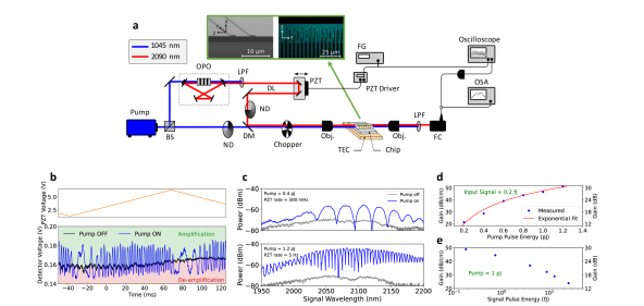
To fabricate the device, we use a commercial wafer (NANOLN), with a 700-nm-thick X-cut MgO-doped LN thin-film on 2-m-thick SiO2. We start with periodic poling of the chip followed by waveguide patterning and dry etching with Ar+ plasma. Insets of Fig. 2a show a scanning electron microscope (SEM) image of a pair of waveguides near the chip facet, and a second-harmonic microscope image of the periodic poling before waveguide etching. Additional fabrication details are included in Supplement 1, Section 5.
3 Results and Discussion
3.1 Optical Parametric Amplification
We measured the small-signal gain of a 6-mm-long dispersion-engineered periodically poled lithium niobate (PPLN) waveguide with the setup shown in Fig. 2a. The chip temperature was set to C using a thermoelectric cooling stage (TEC) to optimize the phase matching condition. The OPA pump pulses are ~75-fs-long, from a mode-locked fiber laser centered at 1045 nm. The signal pulses are ~35-fs-long centered at 2090 nm generated from a table-top degenerate optical parametric oscillator [29]. The pump and signal pulses are coupled into the same PPLN waveguide using a reflective objective. The phase difference between pump and signal is scanned by a piezoelectric transducer (PZT) in a delay arm, and the transmitted signal is measured with a 2 m detector followed by an oscilloscope (Fig. 2b). The ripples show the entire pulse being amplified and de-amplified as the phase of the signal is scanned. We also measured the spectra with an optical spectrum analyzer (OSA) for the two cases of pump on and pump off (Fig. 2c), with an acquisition time for the OSA being much longer than the periodicity of the phase scan. The ripples in the spectrum with the pump on again confirm the phase-sensitive amplification of the broadband signal.
We also scan the pump power and record the maximum gain in the measured spectra. Figure 2d shows this gain along with the expected exponential response exhibiting a maximum parametric gain of ~30 dB (~50 dB/cm) on the chip for a pump pulse energy of just 1.2 pJ in the waveguide. The agreement with the theoretical estimate suggests that the low-pump-depletion approximation is still valid and larger gain values are available by a further increase in pump energy (Supplement 1, Section 3).
Figure 2e shows the behavior of gain vs input signal energy for a pump pulse energy of 1 pJ. The decrease in gain over the entire measured range indicates that the gain is already saturating even for input signal energies as low as 0.2 fJ, which is the lowest energy that we could accurately measure in our setup. This suggest that the amplifier can provide larger levels of gain for signal energies in the aJ range. We explore this possibility in the next section.
3.2 Optical Parametric Generation
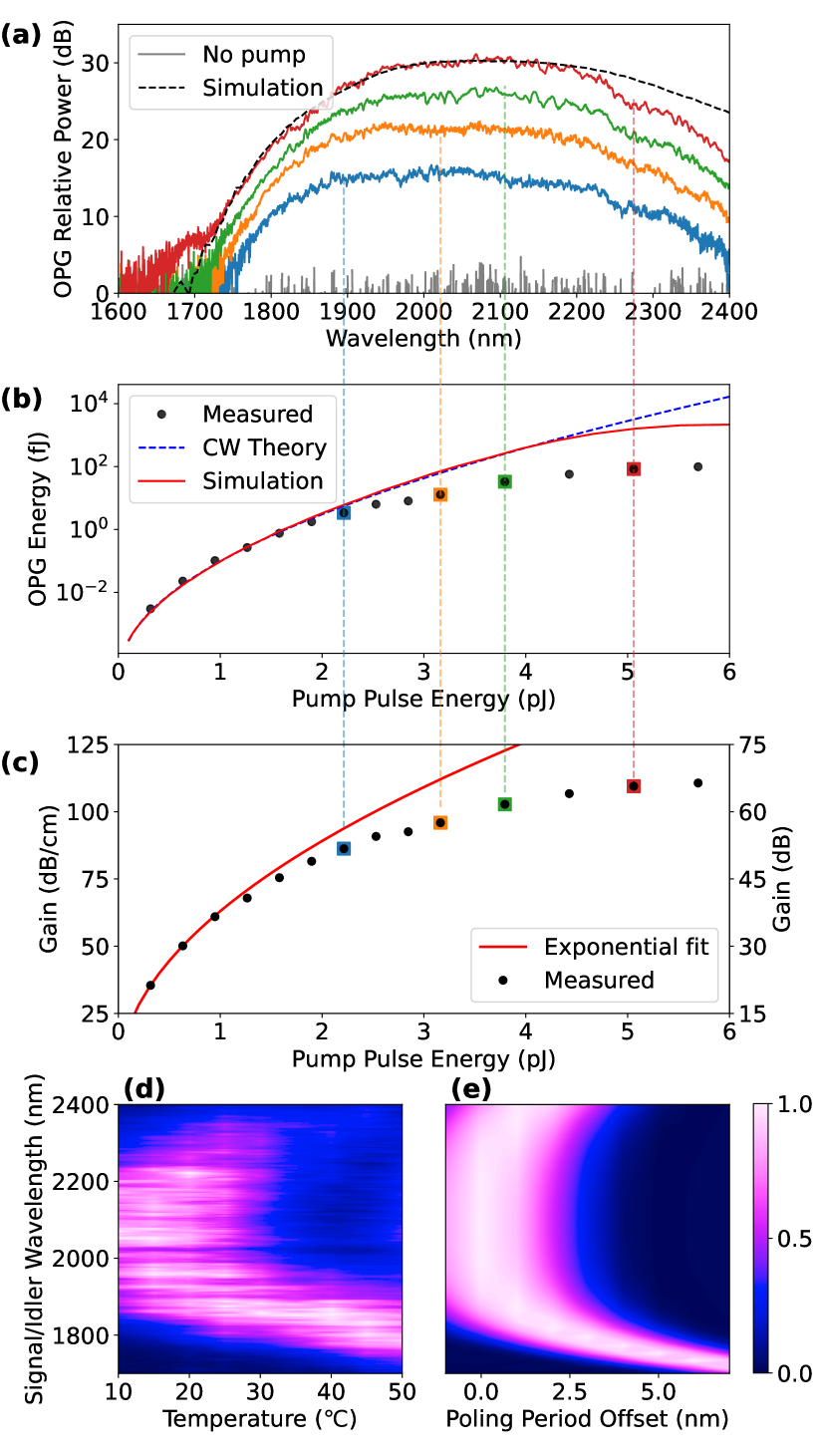
To measure the largest possible bandwidth and unsaturated gain in our dispersion-engineered PPLN waveguides, we removed the input signal (leaving only vacuum fluctuations present near the 2 m signal wavelength). When the gain of an OPA is large, spontaneously generated signal photons can grow to macroscopic levels in a process known as parametric superfluorescence or optical parametric generation (OPG), with an expected number of photons at the output given by [30] . For a fixed device length, the rate of growth of OPG pulse energy versus pump pulse energy can be used to extract the OPA gain as follows. The number of OPG photons is , which for parametric gains larger than ~10 dB can be approximated well by . The OPG energy is proportional to , so we have , where is the overall detection efficiency (including output coupling losses) and is a constant that depends on factors such as the input coupling losses, pump peak-to-average power ratio, waveguide length, and waveguide nonlinear efficiency. We have also assumed that within the gain-bandwidth. The measured OPG energy can be fitted to an exponential versus to extract and . This leads to an estimated OPA gain for degenerate operation given by (see Supplement 1, Section 4 for a comparison between this simplified model and full short-pulse simulations). This method of characterization has the additional advantage of not requiring a coherent input signal, hence the output pulses reveal the full gain bandwidth of the amplifier. Removing the input signal also maximizes the dynamic range of operation of the OPA, eliminating gain saturation effects for a large range of pump levels up to the OPG threshold. For larger pump energies, it is possible to operate the OPG in the saturated regime where high efficiency broadband downconversion can be followed by spectral broadening [31].
We characterized our 6-mm-long waveguide through an OPG measurement using the setup from Fig. 2a without the input signal path to the chip (more details in Supplement 1, Section 7). Figure 3a shows several measured output spectra for different pump pulse energies along with a simulated spectra from a wideband nonlinear envelope equation solver seeded with semi-classical quantum noise (see Supplement 1, Sections 2 and 4). The total measured gain bandwidth (at 10 dB below the peak) exceeds 600 nm. The output OPG pulse energy as a function of the pump pulse energy in the waveguide is displayed in Fig. 3b. The exponential growth of the signal as a function of pump pulse energy is used to accurately extract the parametric gain as described above.
The extracted gain is shown in Fig. 3c, exceeding 66 dB on the chip for the 6-mm-long waveguide (110 dB/cm) with less than 6 pJ of estimated pump pulse energy in the waveguide. The departure from the exponential trend at higher pump powers happens before the 10% pump depletion level (see Supplement 1, Section 4) and it is likely the result of other nonlinear effects that become relevant at high gain regimes, including loss through parasitic green generation and scattering. Further studies are necessary to identify and inhibit such processes, but it is important to note that these issues do not limit the use of the amplifier since gain levels beyond 50 dB are reached before entering this region.
Figure 3d shows the measured OPG spectrum as a function of the chip temperature. This measurement is compared with the theoretical OPA gain as a function of poling period shown in Fig. 3e (see Supplement 1, Section 1), confirming the transition from broadband degenerate to narrowband non-degenerate regime, which happens above C in the experiment. Achieving OPG in the non-degenerate regime confirms having a phase-insensitive parametric gain with similar magnitude (~100 dB/cm), which can be a useful on-chip resource for quantum and classical photonics [32, 33].
4 Conclusion
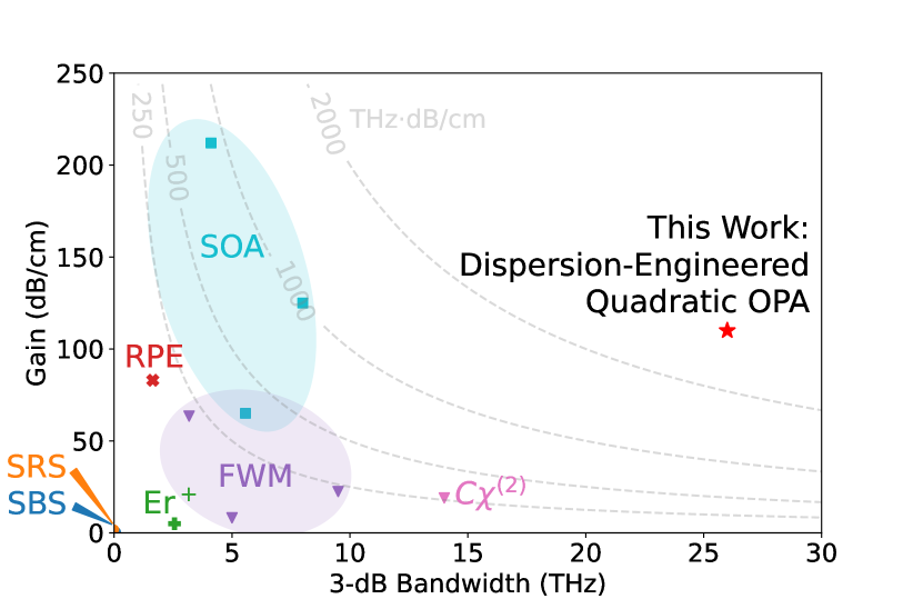
We have demonstrated an on-chip optical parametric amplifier, with gain levels exceeding 30 dB for weak input femtosecond pulses, and 60 dB for vacuum fluctuations, over more than 600 nm of bandwidth around 2 m, using a waveguide that is only 6-mm-long. Furthermore, we have shown that we can operate the amplifier near degeneracy to obtain phase-sensitive amplification. Our results represent a paradigm shift for on-chip optical amplifiers, as shown in Fig. 4. This extraordinary performance of quadratic OPA is achieved by combination of dispersion engineering and quasi-phase matching leading to strong nonlinear interactions owing to spatio-temporal confinement of the pump and signal pulses.
The magnitude of the OPA gain we obtain exceeds the reported gain by cubic nonlinearities and is comparable to what can be achieved with SOAs. The OPA bandwidth is significantly broader than other mechanisms. Currently, the maximum measured gain per unit length is limited by the maximum pump pulse energy that we can safely couple into the waveguide, since the input coupling loss is ~25 dB. (see Supplement 1, Section 7) Improving the coupling loss by more than 10 dB seems feasible by developing integrated spot converters [34]. Such improvement can lead to a gain of more than 150 dB/cm putting the on-chip OPA in direct competition with the largest single-mode SOA gains reported. Further enhancement can be achieved by improving the poling duty cycle, depth, and fidelity [35]. Parametric sweeps confirm that our dispersion engineering is not too sensitive to fabrication variations in waveguide width and etch depth (see Supplement 1, Section 6). Studying the noise behavior of the OPA will be the subject of future work. Combined with other linear and nonlinear functionalities available on thin-film LN, the presented intense OPA can open unprecedented opportunities in integrated photonics, for instance for quantum information processing, mid-infrared sources, optical computing, femtosecond frequency combs and laser ranging.
Funding The authors gratefully acknowledge support from ARO grant no. W911NF-18-1-0285, NSF grant no. 1846273 and 1918549, AFOSR award FA9550-20-1-0040. A part of this research was carried out at the Jet Propulsion Laboratory and the California Institute of Technology under a contract with the National Aeronautics and Space Administration and funded through the President’s and Director’s Research and Development Fund (PDRDF). The authors wish to thank NTT Research for their financial and technical support.
Acknowledgments The device nanofabrication was performed at the Kavli Nanoscience Institute (KNI) at Caltech. The authors thank Robert Gray for his experimental support and Dr. Marc Jankowski for helpful discussions. The authors thank Dr. Joong Hwan Bahng, Dr. Ryan Briggs and Dr. Myoung-Gyun Suh for assistance with the fabrication development process.
Disclosures The authors declare no conflicts of interest.
Data availability Data underlying the results presented in this paper are not publicly available at this time but may be obtained from the authors upon reasonable request.
Supplemental document See Supplement 1 for supporting content.
References
- [1] B. J. Shastri, A. N. Tait, T. Ferreira de Lima, W. H. P. Pernice, H. Bhaskaran, C. D. Wright, and P. R. Prucnal, “Photonics for artificial intelligence and neuromorphic computing,” \JournalTitleNature Photonics 15, 102–114 (2021).
- [2] J. Riemensberger, A. Lukashchuk, M. Karpov, W. Weng, E. Lucas, J. Liu, and T. J. Kippenberg, “Massively parallel coherent laser ranging using a soliton microcomb,” \JournalTitleNature 581, 164–170 (2020).
- [3] Y. Shaked, Y. Michael, R. Z. Vered, L. Bello, M. Rosenbluh, and A. Pe’er, “Lifting the bandwidth limit of optical homodyne measurement with broadband parametric amplification,” \JournalTitleNature Communications 9, 609 (2018).
- [4] Z. Tong, C. Lundström, P. A. Andrekson, C. J. McKinstrie, M. Karlsson, D. J. Blessing, E. Tipsuwannakul, B. J. Puttnam, H. Toda, and L. Grüner-Nielsen, “Towards ultrasensitive optical links enabled by low-noise phase-sensitive amplifiers,” \JournalTitleNature Photonics 5, 430–436 (2011).
- [5] X. Liu, R. M. Osgood, Y. A. Vlasov, and W. M. J. Green, “Mid-infrared optical parametric amplifier using silicon nanophotonic waveguides,” \JournalTitleNature Photonics 4, 557–560 (2010).
- [6] K. J. A. Ooi, D. K. T. Ng, T. Wang, A. K. L. Chee, S. K. Ng, Q. Wang, L. K. Ang, A. M. Agarwal, L. C. Kimerling, and D. T. H. Tan, “Pushing the limits of CMOS optical parametric amplifiers with USRN:Si 7 N 3 above the two-photon absorption edge,” \JournalTitleNature Communications 8, 13878 (2017).
- [7] H. Rong, S. Xu, Y.-H. Kuo, V. Sih, O. Cohen, O. Raday, and M. Paniccia, “Low-threshold continuous-wave Raman silicon laser,” \JournalTitleNature Photonics 1, 232–237 (2007).
- [8] E. A. Kittlaus, H. Shin, and P. T. Rakich, “Large Brillouin amplification in silicon,” \JournalTitleNature Photonics 10, 463–467 (2016).
- [9] B. Haq, S. Kumari, K. V. Gasse, J. Zhang, A. Gocalinska, E. Pelucchi, B. Corbett, and G. Roelkens, “Micro-Transfer-Printed III-V-on-Silicon C-Band Semiconductor Optical Amplifiers,” \JournalTitleLaser & Photonics Reviews 14, 1900364 (2020).
- [10] M. L. Davenport, S. Skendžić, N. Volet, J. C. Hulme, M. J. R. Heck, and J. E. Bowers, “Heterogeneous Silicon/III–V Semiconductor Optical Amplifiers,” \JournalTitleIEEE Journal of Selected Topics in Quantum Electronics 22, 78–88 (2016).
- [11] Z. Yang, M. Jahanbozorgi, D. Jeong, S. Sun, O. Pfister, H. Lee, and X. Yi, “A squeezed quantum microcomb on a chip,” \JournalTitleNature Communications 12, 4781 (2021).
- [12] R. Nehra, R. Sekine, L. Ledezma, Q. Guo, R. M. Gray, A. Roy, and A. Marandi, “Few-cycle vacuum squeezing in nanophotonics,” \JournalTitlearXiv:2201.06768 [quant-ph] (2022).
- [13] M. H. Dunn and M. Ebrahimzadeh, “Parametric Generation of Tunable Light from Continuous-Wave to Femtosecond Pulses,” \JournalTitleScience 286, 1513–1517 (1999).
- [14] Y.-C. Lin, Y. Nabekawa, and K. Midorikawa, “Optical parametric amplification of sub-cycle shortwave infrared pulses,” \JournalTitleNature Communications 11, 3413 (2020).
- [15] G. Cerullo and S. De Silvestri, “Ultrafast optical parametric amplifiers,” \JournalTitleReview of Scientific Instruments 74, 1–18 (2003).
- [16] S.-W. Huang, G. Cirmi, J. Moses, K.-H. Hong, S. Bhardwaj, J. R. Birge, L.-J. Chen, E. Li, B. J. Eggleton, G. Cerullo, and F. X. Kärtner, “High-energy pulse synthesis with sub-cycle waveform control for strong-field physics,” \JournalTitleNature Photonics 5, 475–479 (2011).
- [17] E. J. Stanton, J. Chiles, N. Nader, G. Moody, G. Moody, N. Volet, L. Chang, J. E. Bowers, S. W. Nam, and R. P. Mirin, “Efficient second harmonic generation in nanophotonic GaAs-on-insulator waveguides,” \JournalTitleOptics Express 28, 9521–9532 (2020).
- [18] D. M. Lukin, C. Dory, M. A. Guidry, K. Y. Yang, S. D. Mishra, R. Trivedi, M. Radulaski, S. Sun, D. Vercruysse, G. H. Ahn, and J. Vučković, “4H-silicon-carbide-on-insulator for integrated quantum and nonlinear photonics,” \JournalTitleNature Photonics 14, 330–334 (2020).
- [19] D. J. Wilson, K. Schneider, S. Hönl, M. Anderson, Y. Baumgartner, L. Czornomaz, T. J. Kippenberg, and P. Seidler, “Integrated gallium phosphide nonlinear photonics,” \JournalTitleNature Photonics 14, 57–62 (2020).
- [20] A. W. Bruch, X. Liu, Z. Gong, J. B. Surya, M. Li, C.-L. Zou, and H. X. Tang, “Pockels soliton microcomb,” \JournalTitleNature Photonics 15, 21–27 (2021).
- [21] C. Wang, C. Langrock, A. Marandi, M. Jankowski, M. Zhang, B. Desiatov, M. M. Fejer, and M. Lončar, “Ultrahigh-efficiency wavelength conversion in nanophotonic periodically poled lithium niobate waveguides,” \JournalTitleOptica 5, 1438–1441 (2018).
- [22] M. Jankowski, C. Langrock, B. Desiatov, A. Marandi, C. Wang, M. Zhang, C. R. Phillips, M. Lončar, and M. M. Fejer, “Ultrabroadband nonlinear optics in nanophotonic periodically poled lithium niobate waveguides,” \JournalTitleOptica 7, 40–46 (2020).
- [23] M. Zhang, B. Buscaino, C. Wang, A. Shams-Ansari, C. Reimer, R. Zhu, J. M. Kahn, and M. Lončar, “Broadband electro-optic frequency comb generation in a lithium niobate microring resonator,” \JournalTitleNature 568, 373–377 (2019).
- [24] C. Wang, M. Zhang, X. Chen, M. Bertrand, A. Shams-Ansari, S. Chandrasekhar, P. Winzer, and M. Lončar, “Integrated lithium niobate electro-optic modulators operating at CMOS-compatible voltages,” \JournalTitleNature 562, 101 (2018).
- [25] T. P. McKenna, H. S. Stokowski, V. Ansari, J. Mishra, M. Jankowski, C. J. Sarabalis, J. F. Herrmann, C. Langrock, M. M. Fejer, and A. H. Safavi-Naeini, “Ultra-low-power second-order nonlinear optics on a chip,” \JournalTitlearXiv:2102.05617 [physics, physics:quant-ph] (2021).
- [26] J. Lu, A. A. Sayem, Z. Gong, J. B. Surya, C.-L. Zou, and H. X. Tang, “Ultralow-threshold thin-film lithium niobate optical parametric oscillator,” \JournalTitlearXiv:2101.04735 [physics] (2021).
- [27] J. Zhao, C. Ma, M. Rüsing, and S. Mookherjea, “High Quality Entangled Photon Pair Generation in Periodically Poled Thin-Film Lithium Niobate Waveguides,” \JournalTitlePhysical Review Letters 124, 163603 (2020).
- [28] R. Luo, Y. He, H. Liang, M. Li, and Q. Lin, “Highly tunable efficient second-harmonic generation in a lithium niobate nanophotonic waveguide,” \JournalTitleOptica 5, 1006–1011 (2018).
- [29] A. Marandi, K. A. Ingold, M. Jankowski, and R. L. Byer, “Cascaded half-harmonic generation of femtosecond frequency combs in the mid-infrared,” \JournalTitleOptica 3, 324–327 (2016).
- [30] W. H. Louisell, A. Yariv, and A. E. Siegman, “Quantum Fluctuations and Noise in Parametric Processes. I.” \JournalTitlePhysical Review 124, 1646–1654 (1961).
- [31] M. Jankowski, N. Jornod, C. Langrock, B. Desiatov, A. Marandi, M. Lončar, and M. M. Fejer, “Efficient Octave-Spanning Parametric Down-Conversion at the Picojoule Level,” \JournalTitlearXiv:2104.07928 [physics] (2021). ArXiv: 2104.07928.
- [32] Z. Y. Ou, S. F. Pereira, H. J. Kimble, and K. C. Peng, “Realization of the Einstein-Podolsky-Rosen paradox for continuous variables,” \JournalTitlePhysical Review Letters 68, 3663–3666 (1992).
- [33] J. Hansryd, P. A. Andrekson, M. Westlund, Jie Li, and P. Hedekvist, “Fiber-based optical parametric amplifiers and their applications,” \JournalTitleIEEE Journal of Selected Topics in Quantum Electronics 8, 506–520 (2002).
- [34] N. Yao, N. Yao, J. Zhou, J. Zhou, J. Zhou, R. Gao, R. Gao, J. Lin, J. Lin, J. Lin, M. Wang, M. Wang, Y. Cheng, Y. Cheng, Y. Cheng, Y. Cheng, Y. Cheng, Y. Cheng, Y. Cheng, W. Fang, W. Fang, and L. Tong, “Efficient light coupling between an ultra-low loss lithium niobate waveguide and an adiabatically tapered single mode optical fiber,” \JournalTitleOptics Express 28, 12416–12423 (2020).
- [35] M. Rüsing, J. Zhao, and S. Mookherjea, “Second harmonic microscopy of poled x-cut thin film lithium niobate: Understanding the contrast mechanism,” \JournalTitleJournal of Applied Physics 126, 114105 (2019).