Supplemental Material: Band gap widening and behavior of Raman-active phonon modes of cubic single-crystalline (In,Ga)2O3 alloy films
Johannes Feldl
Paul-Drude-Institut für Festkörperelektronik, Leibniz-Institut im Forschungsverbund Berlin e. V., Hausvogteiplatz 5–7, 10117 Berlin, Germany
Martin Feneberg
Institut für Physik, Otto-von-Guericke-Universität Magdeburg, Universitätsplatz 2, 39106 Magdeburg, Germany
Alexandra Papadogianni
Jonas Lähnemann
Paul-Drude-Institut für Festkörperelektronik, Leibniz-Institut im Forschungsverbund Berlin e. V., Hausvogteiplatz 5–7, 10117 Berlin, Germany
Takahiro Nagata
National Institute for Materials Science, Tsukuba, Ibaraki 305-0044, Japan
Oliver Bierwagen
Paul-Drude-Institut für Festkörperelektronik, Leibniz-Institut im Forschungsverbund Berlin e. V., Hausvogteiplatz 5–7, 10117 Berlin, Germany
Rüdiger Goldhahn
Institut für Physik, Otto-von-Guericke-Universität Magdeburg, Universitätsplatz 2, 39106 Magdeburg, Germany
Manfred Ramsteiner
ramsteiner@pdi-berlin.dePaul-Drude-Institut für Festkörperelektronik, Leibniz-Institut im Forschungsverbund Berlin e. V., Hausvogteiplatz 5–7, 10117 Berlin, Germany
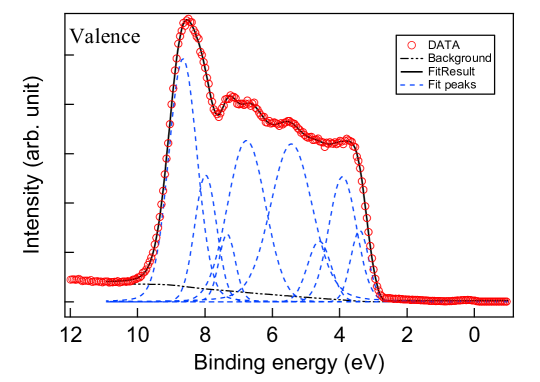
For our investigation of the electronic state of the (In,Ga)2O3 alloy we employed hard X-ray photoelectron spectroscopy (HAXPES) with keV. The corresponding inelastic mean free path (IMFP: ) of HAXPES for the In 3d core-level photoemission calculated by the Tanuma-Powell-Penn-2M(Tanuma, 2006) is nm. Therefore, our HAXPES measurements probed approximately 21 nm (probing depth: IMFP(Powell et al., 1999; Tanuma, 2006)) below the sample surface, which can reduce the effect of the surface Fermi level pinning of In2O3.
In this paper, we use the multi-peak fitting for the valence band region, as shown in Fig. S1. By using the base peaks based on the Voigt function, we first fitted the valence band structure. Then, by considering the in-gap state and energy resolution (wid) using the Fermi edge fitting function
(S1)
the valence band maximum value (pos) was estimated. Here, denotes the binding energy and the total fit is described by:
(S2)
with intensity offset FE_offset.
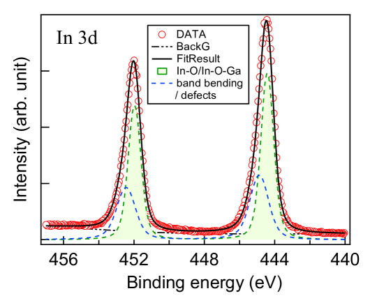
The In 3d core-level spectra consist of In-O/In-O-Ga bonds and the effects of band bending corresponding to the Fermi level pinning and defective InOx bonds. To simplify these bonding states, we used two peaks for fitting of the In 3d core-level spectrum, as shown in Fig. S2.
Figure S1: HAXPES valence band data and corresponding Voigt multiple-peak fitting functions. The Fermi energy corresponds to an energy of 0 eV.
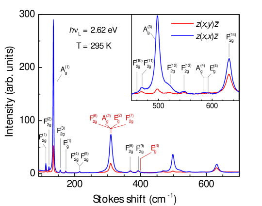
For the assignment of the observed phonon lines, polarized Raman spectra were acquired at room-temperature for In2O3 bulk crystals with an excitation wavelength of 473 nm. While a parallel configuration allows for all modes (, and ) to be detected, a crossed configuration strongly suppresses modes while leaving ones mostly not affected.(Kranert et al., 2014) The remaining contribution of the modes most likely results from an imperfect alignment of the waveplates as well as a mixed output laser polarization. Fig. S3 shows such polarization dependent measurements. Note that in the indicated scattering configurations corresponds to the [111] crystal orientation, whereas and are two orthogonal directions in the {111} plane.(Kranert et al., 2014) Not all expected modes are detectable under the presented experimental conditions or can be resolved unambiguously. These modes are displayed with a red label in Fig. S3. The inset of Fig. S3 shows a magnification of the high frequency modes. Here, a very weak but reproducible peak in the binary In2O3 bulk sample appears at 585 cm-1 for the configuration. Hence, we assign this peak to the symmetry.
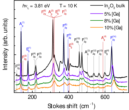
Complementary to the main text, Fig. S4 shows low-temperature (10 K) Raman spectra which resemble the ones measured at room-temperature. However, the phonon lines are blueshifted and exhibit a smaller linewidth at 10 K.
Figure S2: In 3d core-level spectrum with corresponding two-peaks fitting functions. The binding energy is given relative to the Fermi level.Figure S3: Polarization dependent Raman measurements for the symmetry determination of the phonon modes. Modes which could not be identified unambiguously or are not present under the given experimental conditions are marked with red labels. The inset shows a magnification of the high frequency spectra.Figure S4: Low-temperature (10 K) Raman spectra of (In1-xGax)2O3 films for different nominal Ga contents and a reference In2O3 bulk sample excited at a photon energy of 3.81 eV. The phonon modes marked by blue vertical lines and labels are the ones best suited for investigations on (In1-xGax)2O3 films at room-temperature. The remaining modes are marked by black color, except for those, not present in any of the samples under the given experimental conditions or whose symmetry identification was not unambiguous, marked in red.
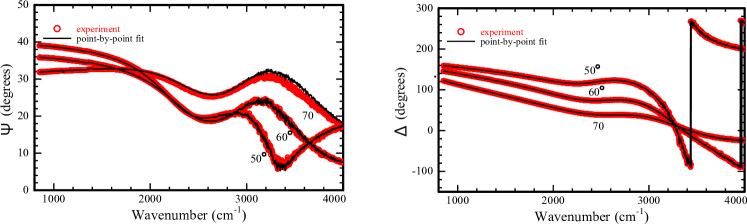
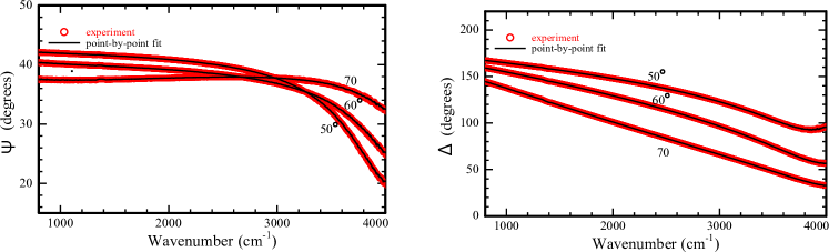
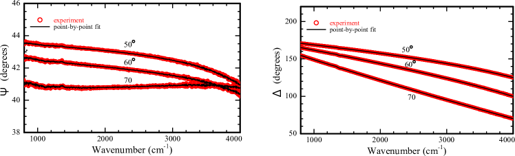
In addition, we present the point-by-point fits to raw ellipsometric data and . For the (In,Ga)2O3:Sn sample, Fig. S5, Fig. S6 and Fig. S7 show the infrared data for the as-grown, oxygen-annealed and vacuum-annealed sample, respectively.
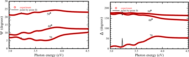
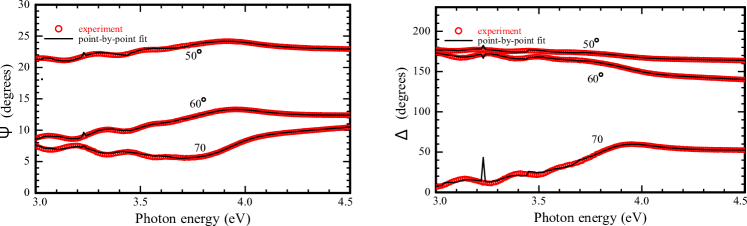
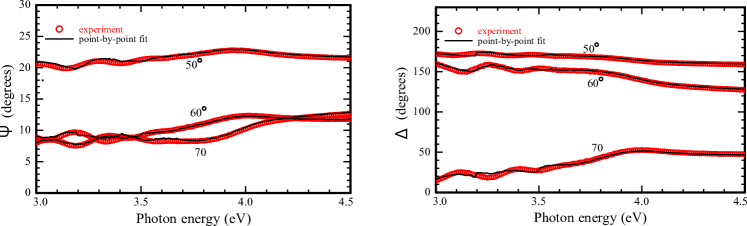
Corresponding data for the visible & UV spectral range can be found in Fig. S8, Fig. S9 and Fig. S10 for the thin films with Ga content of 0.05, 0.08 and 0.1 respectively. The surface roughness layer thicknesses obtained by model fitting agree well with the atomic force microscopy data presented by Papadogianni e. al.(Papadogianni et al., 2021)
Figure S5: Infrared point-by-point fit of raw ellipsometric data and of the as-grown (In,Ga)2O3:Sn with a carrier concentration of cm-3.Figure S6: Infrared point-by-point fit of raw ellipsometric data and of the oxygen-annealed (In,Ga)2O3:Sn with a carrier concentration of cm-3.Figure S7: Infrared point-by-point fit of raw ellipsometric data and of the vacuum-annealed (In,Ga)2O3:Sn with a carrier concentration of cm-3.Figure S8: Point-by-point fits of raw ellipsometric data and in the visible & UV spectral range for the thin film with . A surface roughness layer of 3.0 nm was obtained.Figure S9: Point-by-point fits of raw ellipsometric data and in the visible & UV spectral range for the thin film with . A surface roughness layer of 3.3 nm was obtained.Figure S10: Point-by-point fits of raw ellipsometric data and in the visible & UV spectral range for the thin film with . A surface roughness layer of 7.5 nm was obtained.
Papadogianni et al. (2021)A. Papadogianni, C. Wouters, R. Schewski,
J. Feldl, J. Lähnemann, T. Nagata, E. Kluth, M. Feneberg, R. Goldhahn, M. Ramsteiner, M. Albrecht, and O. Bierwagen, ArXiv210609612 Cond-Mat (2021), arXiv:2106.09612 [cond-mat]
.