Multiple energy scales and anisotropic energy gap in the charge-density-wave phase of kagome superconductor CsV3Sb5
Abstract
Kagome metals V3Sb5 ( = K, Rb, and Cs) exhibit superconductivity at 0.9-2.5 K and charge-density wave (CDW) at 78-103 K. Key electronic states associated with the CDW and superconductivity remain elusive. Here, we investigate low-energy excitations of CsV3Sb5 by angle-resolved photoemission spectroscopy. We found an energy gap of 50-70 meV at the Dirac-crossing points of linearly dispersive bands, pointing to an importance of spin-orbit coupling. We also found a signature of strongly Fermi-surface and momentum-dependent CDW gap characterized by the larger energy gap of maximally 70 meV for a band forming a saddle point around the M point, the smaller (0-18 meV) gap for a band forming massive Dirac cones, and a zero gap at the /A-centered electron pocket. The observed highly anisotropic CDW gap which is enhanced around the M point signifies an importance of scattering channel connecting the saddle points, laying foundation for understanding the nature of CDW and superconductivity in V3Sb5.
pacs:
71.18.+y, 71.20.-b, 79.60.-iKagome lattice, consisting of transition metal ions with two-dimensional (2D) network of corner-sharing triangles, provides an excellent platform to explore novel quantum phenomena originating from electron correlation and nontrivial band topology. While insulating kagome lattice has been intensively studied in relation to geometric frustration and quantum magnetism RamirezARMS1994 ; ShoresJACS2005 ; PollmannPRL2008 ; BalentsNature2010 ; YanScience2011 ; HanNature2012 ; HanPRL2012 ; FuScience2015 , metallic kagome lattice is currently attracting particular attention because of its unique band structure characterized by the nearly flat band and Dirac-cone band that promote strong-correlation and topological effects. Depending on the electron filling of the kagome-lattice bands, various intriguing quantum states have been predicted, e.g. Weyl magnet NayakSA2016 ; YangNJP2017 ; KurodaNM2017 ; YeNature2018 ; LiuNP2018 ; MoraliScience2019 ; LiuScience2019 , density wave orders IsakovPRL2006 ; GuoPRB2009 ; WangPRB2013 , charge fractionalization OBrienPRB2010 ; RueggPRB2011 , and superconductivity WangPRB2013 ; KoPRB2009 ; KieselPRB2012 ; KieselPRL2013 .
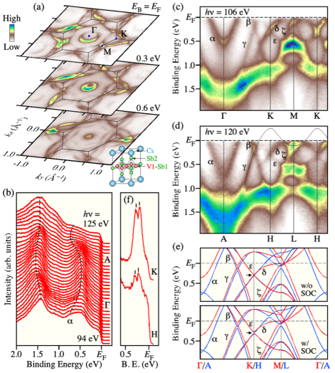
Recently, a family of V3Sb5 ( = K, Rb, and Cs) was discovered to be a kagome superconductor OrtizPRM2019 ; OrtizPRL2020 ; OrtizPRM2021 with superconducting transition temperature of 0.93-2.5 K, despite the fact that kagome metals rarely become a superconductor. V3Sb5 crystallizes in a layered structure consisting of alternately stacked V kagome-lattice layer with hexagonally arranged Sb atoms (V1 and Sb1), graphene-like Sb layer (Sb2), and hexagonal layer [see Fig. 1(a)]. Besides superconductivity, V3Sb5 commonly undergoes a charge-density wave (CDW) transition at = 78-103 K accompanied with three-dimensional (3D) 222 charge order LiAX2021 ; LiangAX2021 . Angle-resolved photoemission spectroscopy (ARPES) clarified that the kagome-lattice bands participate in the states near the Fermi level (), by observing the Dirac-cone-like bands forming a large hexagonal Fermi surface (FS) centered at the point and a saddle point near at the M point, together with an electron pocket at the point of 2D Brillouin zone (BZ), consistent with the density-functional-theory (DFT) calculations OrtizPRL2020 ; YangSA2020 ; LiAX2021 ; LiuAX2021 .
While overall electronic structure of V3Sb5 is almost established, the mechanism of superconductivity and CDW is highly controversial. topological invariant in the normal state suggested by the DFT calculation OrtizPRL2020 ; OrtizPRM2021 may point to unconventional (topological) superconductivity. Existence of a saddle point in the calculated band structure was discussed to promote the -wave pairing associated with the scattering between saddle points via = (, 0) vector NandkishoreNP2012 . Weak electron-phonon coupling suggested by the DFT calculation TanAX2021 also supports an unconventional pairing. In the experiment, conventional vs. unconventional nature of superconductivity is far from reaching a consensus, as represented by contradictory reports on the presence/absence of gap nodes DuanAX2021 ; CZhaoAX2021 . And very recently, a nematic electronic state and a two-fold symmetry superconductivity was observed in CsV3Sb5 Xiang AX2021 .
The electronic states relevant to the CDW formation are also under intensive debate. Apparent CDW-gap opening was not observed in previous ARPES studies on RbV3Sb5 and CsV3Sb5 OrtizPRL2020 ; LiuAX2021 , whereas scanning tunneling microscopy/spectroscopy (STM/STS) on KV3Sb5 and CsV3Sb5 reported a gap opening JiangAX2020 ; ChenAX2021 ; HZhaoAX2021 . While the calculation suggested that the CDW is triggered by the Peierls instability due to the FS nesting TanAX2021 , x-ray scattering on RbV3Sb5 and CsV3Sb5 suggested an electronic-driven mechanism because of the absence of expected phonon anomaly LiAX2021 . In contrast, optical spectroscopy on CsV3Sb5 suggested the FS-nesting mechanism by observing the reduction of Drude weight below for the saddle-point-related feature ZhouAX2021 . Thus, the mechanism of CDW and superconductivity is still far from being established.
In this article, we report a high-resolution ARPES study of CsV3Sb5 single crystals. We established the low-energy excitations in the CDW phase, and found (i) the gap opening at the Dirac points due to the spin-orbit coupling (SOC) and (ii) the strongly FS and momentum () dependent CDW gap characterized by multiple energy scales. We discuss implications of the present results in relation to the mechanism of CDW and superconductivity in V3Sb5.
We at first present the overall band structure of CsV3Sb5 (see Supplemental Material for details of the experimental condition and the band-calculation method SM ). Figure 1(a) shows the ARPES-intensity map at representative binding energy () slices as a function of and , obtained with 106-eV photons which probe the 0 plane of the bulk BZ [the value was determined by the periodicity of band dispersion as a function of photon energy (); variation of the band in the normal-emission measurement is highlighted in Fig. 1(b) and Supplementary Fig. 5 SM ]. We found that the overall intensity pattern in Fig. 1(a) is consistent with the previous ARPES reports on V3Sb5 OrtizPRL2020 ; YangSA2020 ; LiAX2021 ; LiuAX2021 . One can identify a circular pocket centered at the point. This pocket originates from an electron band (called here the band) as visible from ARPES-intensity plot along the KM cut in Fig. 1(c). According to the DFT calculations LiuAX2021 ; JiangAX2020 ; JZhaoAX2021 , this band is attributed to the band of Sb1 atoms embedded in the kagome-lattice plane. One can recognize in Fig. 1(a) triangular shaped intensity pattern centered at each K point which connects to each other around the M point and forms a large hexagonal FS centered at the point. As shown in Fig. 1(c), this pocket originates from a band located at 1 eV at the K point (the band) that displays an overall linear dispersion toward on approaching the point and crosses at of the K interval. This band is reproduced in the calculation in Fig. 1(e) and attributed to the kagome-lattice band with mainly V- character LiuAX2021 ; JZhaoAX2021 . This band intersects other two linearly dispersive bands ( and bands) at 0.1 eV and 0.5 eV, and the band also intersects the linearly dispersive band at the K point, forming multiple Dirac points (note that the Dirac point associated with the - band crossing is predicted to form a nodal line along when the SOC is neglected JZhaoAX2021 ). The band rapidly disperses toward on approaching the M point and participates in forming the saddle point. At the M point, there is another holelike band ( band) with the top of dispersion below .
At = 120 eV that corresponds to the = plane, there are several similarities in the band dispersions with those at the = 0 plane, e.g. linear dispersions of the , , , and bands and their Dirac-cone formation [compare Figs. 1(c) and 1(d)]. Besides such similarities, one can recognize a clear difference in energy position of the -band bottom, i.e. it is located at 0.5 and 0.75 eV at = 0 and , respectively. One can also find that a shallow electron pocket centered at the L point appears only at the = plane. According to the calculation [Fig. 1(e)], this band is connected to the band as indicated by a guide in Fig. 1(d). The observed band structures including finite dispersions reasonably agree with the bulk band calculation, supporting their bulk nature. It is noted that, while the existence of topological surface state at the point was predicted OrtizPRL2020 ; OrtizPRM2021 , we found no evidence for such a surface state below .
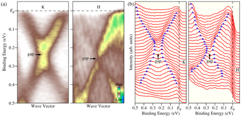
As shown in Fig. 1(c), the intensity of the band is weakened at which the band intersects at the K point at 0.3 eV. This is also the case for the band-crossing point at the H point [Fig. 1(d)]. To better visualize the band modulation associated with the intensity weakening, we plot in Fig. 1(f) the EDCs at the K and H points. These EDCs commonly exhibit two-peaked structure around the Dirac point, signifying an energy gap (called Dirac gap; see also Fig. 6 of Supplemental Material SM ). From the energy separation of two peaks, we have estimated the magnitude of Dirac gap to be 50-70 meV. The Dirac gap is associated with the SOC because the calculations predict a spin-orbit gap at the Dirac point (note that, by referring to the calculation without SOC, the gap at the K and H points is purely of SOC origin, whereas those at other k points are additionally affected by the band hybridization). Given the fact that some Dirac points are predicted to be located at very close to in V3Sb5 OrtizPRM2019 , our observation suggests that the SOC needs to be taken into account when the connection between the Dirac-fermion and transport properties (such as anomalous Hall effect YangSA2020 ; YuAX2021 ) is discussed.
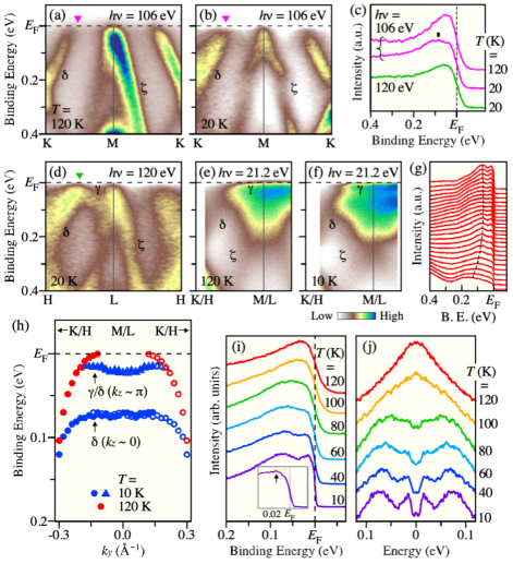
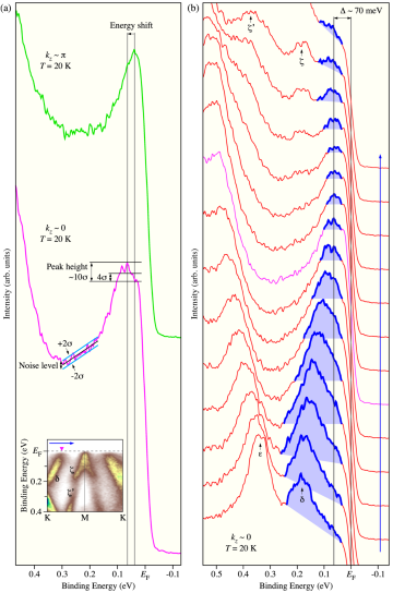
Next we present the electronic states associated with the CDW. Figures 2(a) and 2(b) show the ARPES-intensity plot near measured along the MK cut at temperature above (120 K) and below (20 K) , respectively. In the normal state [Fig. 2(a)], the band crosses at the midway of the MK line and forms a saddle point slightly above at the M point. There also exists the band which forms another saddle point at the M point, while it does not cross along the MK cut. In the CDW phase [Fig. 2(b)], the intensity of the band is modulated at 0.2 eV likely due to band hybridization by CDW. More importantly, a hump structure at 70 meV is observed at the kF point of the band [see magenta curves in Fig. 2(c); see also Fig. 7 of Supplementary Material SM ]. Since the kF point of the band is well isolated from the -band top, the 70-meV hump is unlikely attributed to the saddle point of the band but most probably reflects a CDW-gap opening on the band. To clarify the 3D nature of CDW, the near- ARPES intensity at 20 K along the LH cut is plotted in Fig. 2(d). Here, a shallow electron pocket is seen around near the kF point of the band. Intriguingly, unlike the MK cut, EDC near kF of the / band does not show a clear hump structure [green curve in Fig. 2(c)], suggesting the bulk origin of the hump structure and the reduction of the CDW-gap size around the LH line.
To gain further insights into the electronic structure in the CDW phase, we have performed higher-resolution ( = 7 meV) measurements by utilizing low-energy photons ( = 21.2 eV) [Figs. 2(e)-2(f)]. We found that, while 21.2-eV photons are expected to probe 0.8 by referring to the estimated value, the ARPES data simultaneously reflect the band structures at around = 0 and due to a broadening effect (for details, see Fig. 8 of Supplemental Material SM ). In the CDW phase, one can see a broad hump in the EDCs at 150 meV around the K/H point [dashed curve in Fig. 2(g)] which disperses toward on approaching the M/L point and stays at 70 meV around the M/L point to form a nearly flat band. This hump feature is attributed to the gapped band at = 0 seen in Figs. 2(b) and 2(c). There exists another sharp peak near , separated from the hump by a dip at 35 meV. This band is assigned to the electron pocket at = with a finite mixture of the band ( = component) near kF. In fact, as shown by a plot of experimental band dispersion at 10 K obtained by tracing the peak position of EDCs in Fig. 2(h), the low-energy branch has an electronlike dispersion. Thus, the characteristic peak-dip-hump structure in the EDCs is attributed to the existence of two types of bands at different ’s, the hump and peak, called here the saddle-point band and Dirac band, respectively. We found that the peak-dip-hump structure vanishes above [Fig. 2(e); for the experimental band dispersion, see red circles in Fig. 2(h)]. To examine whether this change is associated with the CDW, we show in Fig. 2(i) the temperature dependence of EDC at the kF point of Dirac band. The hump survives up to 80 K (below ) and disappears at 100 K (above ), demonstrating that the hump is indeed associated with the formation of CDW and reflects the CDW gap for the saddle-point band.
An important finding manifests itself by a careful inspection of the EDCs in Fig. 2(i). The sharp peak at = 10 K is not located at but at slightly higher (15 meV) as seen from the magnified EDCs in the inset (see arrow). Symmetrized EDC in Fig. 2(j) reveals spectral-weight suppression in the narrow energy region of 15 meV within the sharp peaks, indicative of the small gap opening at the Dirac band (note that this small gap is not resolved in Figs. 2(b) and 2(c) because of insufficient energy resolution for higher ’s). This gap is associated with the CDW, because it is gradually weakened on elevating temperature and disappears above , in accordance with the behavior of saddle-point band at 70 meV. These results indicate that the CDW of CsV3Sb5 is characterized by at least two energy scales.
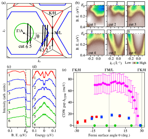
Throughout the whole 2D BZ, we have investigated the CDW gap for the saddle-point and Dirac bands, and found that the gap is strongly k dependent. Figure 3(b) shows the ARPES intensity plotted along several k cuts shown as cuts 1-6 in the FS mapping in Fig. 3(a) which covers the kF points of the shallow electron band (cut 1), the hexagonal pocket associated with the Dirac band (cuts 2-4), and the electron pocket at /A (cuts 5-6). The dip-originated spectral weight suppression, which is a measure of the CDW gap opening for the saddle-point band, is most prominent along cut 1 (MK/LH cut) and gradually becomes less prominent on moving away from the M/L point, as visible from a systematic change in the ARPES intensity along cuts 2-4. We have extracted the EDCs at representative kF points on the Dirac band (points 1-4) in Fig. 3(c), and found that the hump gradually approaches on moving away from the M point. This signifies the strong k dependence of the CDW gap. It is noted that the temperature-induced band energy shift in Fig. 2(h) is another measure of the gap size for the saddle-point band; one can confirm that the band shift becomes smaller (i.e., the gap becomes smaller) as moving away from the M point. The symmetrized EDC at = 10 K in Fig. 3(d) further reveals that the Dirac band near also shows anisotropic CDW gap; the gap is 16 meV at point 1 but it vanishes at point 4 (along the K/AH line). Another important finding is that there exists no obvious spectral anomaly for the /A-centered electron pocket [see cuts 5 and 6 in Fig. 3(b)]. Also, the hump is absent at points 5 and 6 in Figs. 3(c) and 3(d). These results indicate that the CDW gap is absent in the electron pocket at /A. We have estimated the size of CDW gap at = 10 K at various kF points and plotted the as a function of FS angle in Fig. 3(e) (see Fig. 9 of Supplemental Material for a full data set SM ). As clearly seen, the CDW gap is larger for the saddle-point band (maximally 70 meV) and smaller for the Dirac band (maximally 18 meV), whereas it is absent on entire electron pocket at /A. Intriguingly, the CDW gap has a strong anisotropy and takes a maximum around = 0∘ (along the M/AL cut) and a minimum around = 30∘ (along the K/AH cut) for both the saddle-point and Dirac bands.
The ARPES-determined CDW gap has a good correspondence to the unusual behavior in the DOS observed by other spectroscopic techniques. STM/STS reported a broad hump feature at 70 meV and V-shaped DOS within 10-20 meV of at low temperatures JiangAX2020 ; ChenAX2021 ; HZhaoAX2021 . These features likely correspond to the CDW gaps for the saddle-point and Dirac bands, respectively. STM/STS also found residual DOS at zero bias voltage, and it could be contributed from the electron pocket at and the gapless portion of the Dirac band. Recent optical spectroscopy of CsV3Sb5 revealed a marked suppression of the Drude weight below ZhouAX2021 . This would be also related to the CDW gap for the saddle-point band because its energy scale ( 86.5 meV) is similar to the hump energy in ARPES. Thus, our ARPES data definitely help interpreting characteristic spectroscopic signatures seen by other experiments.
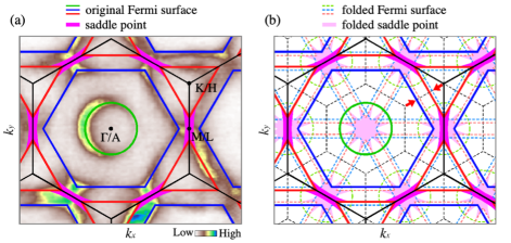
Our observation also sheds light on the mechanism of CDW and superconductivity in V3Sb5. Theoretical studies predicted that the inter-band scattering between saddle points promote CDW or unconventional density waves TanAX2021 ; FengAX2021 , but direct experimental proof was elusive. The observed large CDW gap at the saddle-point band around the point supports this prediction and suggests that the electron scattering via = (, 0) connecting saddle points contributes largely to the energy gain for stabilizing the CDW with in-plane 22 component. To understand this point in more detail, we plot a schematic of the reconstructed FS in Fig.4. Original and folded FSs are indicated by solid and dashed curves, respectively, with orbital-dependent colorings [original FSs were determined by tracing the ARPES intensity at in Fig. 4(a)]. Also, original and folded saddle-point regions of the band are shown by magenta and light magenta paintings, respectively. One can see that original and folded saddle points around the M point overlap well, whereas the FSs along the K cut show a finite mismatch as marked by red arrows. Such a difference in the band/FS overlaps via the 22 vector qualitatively explains the observed CDW-gap anisotropy; the gap size is larger around the M point due to the overlap of the original and folded saddle points. A remaining issue is the origin of additional 3D component of CDW (with 222 periodicity), which is puzzling because the CDW vector connects the M point to the L point where no saddle point exists. This necessitates further selective experiments. It is also predicted that the scattering between saddle points may promote unconventional superconductivity, depending on the degree of competition with CDW NandkishoreNP2012 . However, the observed large CDW gap suggests substantial reduction of DOS responsible for the superconducting pairing on the saddle-point band. Microscopic theories of superconductivity must be constructed based on such a largely gapped saddle-point band and the CDW-gap nodes for the Dirac bands. In this regard, one can even suggest that major superconducting carriers could originate from the Sb bands at the point rather than the V bands participating in the 2D kagome network.
In conclusion, the present ARPES study of CsV3Sb5 has revealed two key signatures in the band structure, (i) the energy gap on the multiple Dirac points due to the SOC, and (ii) the modification of band structure associated with the CDW-gap opening. We found that the CDW-induced band modification is categorized into three types, the larger CDW gap for the saddle point around the M point, the smaller CDW gap for the Dirac band, and the absence of CDW gap for the electron band at /A. The CDW gap also displays a strong anisotropy. The present result opens a pathway toward understanding the mechanisms of CDW and superconductivity in V3Sb5.
Note Added: During the preparation of this manuscript, we became aware of WangAX2021 , which also reports a CDW gap opening on CsV3Sb5.
Acknowledgements.
This work was supported by JST-CREST (No. JPMJCR18T1), JST-PRESTO (No. JPMJPR18L7), and Grant-in-Aid for Scientific Research (JSPS KAKENHI Grant No. JP17H01139, JP18H01160). The work at Beijing was supported by the National Key R&D Program of China (Grant No. 2020YFA0308800), the Natural Science Foundation of China (Grant No. 92065109), the Beijing Natural Science Foundation (Grant No. Z190006), and the Beijing Institute of Technology (BIT) Research Fund Program for Young Scholars (Grant No. 3180012222011). Z.W thanks the Analysis & Testing Center at BIT for assistances in facility support.References
- (1) A. P. Ramirez, Annu. Rev. Mater. Sci. 24, 453-480 (1994).
- (2) M. P Shores, E. A Nytko, B. M. Bartlett, and D. G. Nocera, J. Am. Chem. Soc. 127, 13462-13463 (2005).
- (3) F. Pollmann, P. Fulde, and K. Shtengel, Phys. Rev. Lett. 100, 136404 (2008).
- (4) L. Balents, Nature 464, 199-208 (2010).
- (5) S. Yan, D. A. Huse, and S. R. White, Science 332, 1173-1176 (2011).
- (6) T.-H. Han, J. S. Helton, S. Chu, D. G. Nocera, J. A. Rodriguez-Rivera, C. Broholm, and Y. S. Lee, Nature 492, 406-410 (2012).
- (7) T. Han, S. Chu, and Y. S. Lee, Phys. Rev. Lett. 108, 157202 (2012).
- (8) M. Fu, T. Imai, T.-H. Han, and Y. S. Lee, Science 350, 655-658 (2015).
- (9) A. K. Nayak, J. E. Fischer, Y. Sun, B. Yan, J. Karel, A. C. Komarek, C. Shekhar, N. Kumar, W. Schnelle, J. K. bler, C. Felser, and S. S. P. Parkin, Sci. Adv. 2, e1501870 (2016).
- (10) H. Yang, Y. Sun, Y. Zhang, W.-J. Shi, S. S. P. Parkin, and B. Yan, New J. Phys. 19, 015008 (2017).
- (11) K. Kuroda, T. Tomita, M.-T. Suzuki, C. Bareille, A. A. Nugroho, P. Goswami, M. Ochi, M. Ikhlas, M. Nakayama, S. Akebi, R. Noguchi, R. Ishii, N. Inami, K. Ono, H. Kumigashira, A. Varykhalov, T. Muro, T. Koretsune, R. Arita, S. Shin, T. Kondo, and S. Nakatsuji, Nat. Mater. 16, 1090-1095 (2017).
- (12) L. Ye, M. Kang, J. Liu, F. v. Cube, C. R. Wicker, T. Suzuki, C. Jozwiak, A. Bostwick, E. Rotenberg, D. C. Bell, L. Fu, R. Comin, and J. G. Checkelsky, Nature 555, 638-642 (2018).
- (13) E. Liu, Y. Sun, N. Kumar, L. Muechler, A. Sun, L. Jiao, S.-Y. Yang, D. Liu, A. Liang, Q. Xu, J. Kroder, V. Sü, H. Borrmann, C. Shekhar, Z. Wang, C. Xi, W. Wang, W. Schnelle, S. Wirth, Y.-L. Chen, S. T. B. Goennenwein, and C. Felser, Nat. Phys. 14, 1125-1131 (2018).
- (14) N. Morali, R. Batabyal, P. K. Nag, E. Liu, Q. Xu, Y. Sun, B. Yan, C. Felser, N. Avraham, and H. Beidenkopf, Science 365, 1286-1291 (2019).
- (15) D. F. Liu, A. J. Liang, E. K. Liu, Q. N. Xu, Y. W. Li, C. Chen, D. Pei, W. J. Shi, S. K. Mo, P. Dudin, T. Kim, C. Cacho, G. Li, Y. Sun, L. X. Yang, Z. K. Liu, S. S. P. Parkin, C. Felser, and Y. L. Chen, Science 365, 1282-1285 (2019).
- (16) S. V. Isakov, S. Wessel, R. G. Melko, K. Sengupta, and Y. B. Kim, Phys. Rev. Lett. 97, 147202 (2006).
- (17) W.-S. Wang, Z.-Z. Li, Y.-Y. Xiang, and Q.-H. Wang, Phys. Rev. B 87, 115135 (2013).
- (18) H.-M. Guo and M. Franz, Phys. Rev. B 80, 113102 (2009).
- (19) A. O’Brien, F. Pollmann, and P. Fulde, Phys. Rev. B 81, 235115 (2010).
- (20) A. Rüegg and G. A. Fiete, Phys. Rev. B 83, 165118 (2011).
- (21) W.-H. Ko, P. A. Lee, and X.-G. Wen, Phys. Rev. B 79, 214502 (2009).
- (22) M. L. Kiesel and R. Thomale, Phys. Rev. B 86, 121105(R) (2012).
- (23) M. L. Kiesel, C. Platt, and R. Thomale, Phys. Rev. Lett. 110, 126405 (2013).
- (24) B. R. Ortiz, L. C. Gomes, J. R. Morey, M. Winiarski, M. Bordelon, J. S. Mangum, I. W. H. Oswald, J. A. Rodriguez-Rivera, J. R. Neilson, S. D. Wilson, E. Ertekin, T. M. McQueen, and E. S. Toberer, Phys. Rev. Mater. 3, 094407 (2019).
- (25) B. R. Ortiz, S. M. L. Teicher, Y. Hu, J. L. Zuo, P. M. Sarte, E. C. Schueller, A. M. Milinda Abeykoon, M. J. Krogstad, S. Rosenkranz, R. Osborn, R. Seshadri, L. Balents, J. He, and S. D. Wilson, Phys. Rev. Lett. 125, 247002 (2020).
- (26) B. R. Ortiz, P. M. Sarte, E. M. Kenney, M. J. Graf, S. M. L. Teicher, R. Seshadri, and S. D. Wilson, Phys. Rev. Mater. 5, 034801 (2021).
- (27) H. X. Li, T. T. Zhang, T. Yilmaz, Y. Y. Pai, C. Marvinney, A. Said, Q. Yin, C. Gong, Z. Tu, E. Vescovo, R. G. Moore, S. Murakami, H. C. Lei, H. N. Lee, B. Lawrie, and H. Miao, arXiv:2103.09769 (2021).
- (28) Z. Liang, X. Hou, W. Ma, F. Zhang, P. Wu, Z. Zhang, F. Yu, J.-J. Ying, K. Jiang, L. Shan, Z. Wang, and X.-H. Chen, arXiv:2103.04760 (2021).
- (29) Z. Liu, N. Zhao, Q. Yin, C. Gong, Z. Tu, M. Li, W. Song, Z. Liu, D. Shen, Y. Huang, K. Liu, H. Lei, and S.-C. Wang, arXiv:2104.01125 (2021).
- (30) S.-Y. Yang, Y. Wang, B. R. Ortiz, D. Liu, J. Gayles, E. Derunova, R. Gonzalez-Hernandez, L. Šmejkal, Y. Chen, S. S. P. Parkin, S. D. Wilson, E. S. Toberer, T. McQueen, and M. N. Ali, Sci. Adv. 6, eabb6003 (2020).
- (31) R. Nandkishore, L. S. Levitov, and A. V. Chubukov, Nat. Phys. 8, 158-163 (2012).
- (32) H. Tan, Y. Liu, Z. Wang, and B. Yan, arXiv:2103.06325 (2021).
- (33) W. Duan, Z. Nie, S. Luo, F. Yu, B. R. Ortiz, L. Yin, H. Su, F. Du, A. Wang, Y. Chen, X. Lu, J. Ying, S. D. Wilson, X. Chen, Y. Song, and H. Yuan, arXiv:2103.11796 (2021).
- (34) C. C. Zhao, L. S. Wang, W. Xia, Q. W. Yin, J. M. Ni, Y. Y. Huang, C. P. Tu, Z. C. Tao, Z. J. Tu, C. S. Gong, H. C. Lei, Y. F. Guo, X. F. Yang, and S. Y. Li, arXiv:2102.08356 (2021).
- (35) Y. Xiang, Q. Li, Y. Li, W. Xie, H. Yang, Z. Wang, Y. Yao, and H. H. Wen, arXiv:2104.06909 (2021).
- (36) Y.-X. Jiang, J.-X. Yin, M. M. Denner, N. Shumiya, B. R. Ortiz, J. He, X. Liu, S. S. Zhang, G. Chang, I. Belopolski, Q. Zhang, M. S. Hossain, T. A. Cochran, D. Multer, M. Litskevich, Z.-J. Cheng, X. P. Yang, Z. Guguchia, G. Xu, Z. Wang, T. Neupert, S. D.Wilson, and M. Z. Hasan, arXiv:2012.15709 (2020).
- (37) H. Chen, H. Yang, B. Hu, Z. Zhao, J. Yuan, Y. Xing, G. Qian, Z. Huang, G. Li, Y. Ye, Q. Yin, C. Gong, Z. Tu, H. Lei, S. Ma, H. Zhang, S. Ni, H. Tan, C. Shen, X. Dong, B. Yan, Z. Wang, and H.-J. Gao, arXiv:2103.09188 (2021).
- (38) H. Zhao, H. Li, B. R. Ortiz, S. M. L. Teicher, T. Park, M. Ye, Z. Wang, L. Balents, S. D. Wilson, and I. Zeljkovic, arXiv:2103.03118 (2021).
- (39) X. Zhou, Y. Li, X. Fan, J. Hao, Y. Dai , Z. Wang , Y. Yao, and H.-H. Wen, arXiv:2104.01015 (2021).
- (40) See Supplemental Material for details of the experimental condition and the band-calculation method, the normal-emission measurements, the SOC-induced Dirac-gap opening, the hump structure at 70 meV in the CDW phase, -broadening effect, and a full set of ARPES intensities and EDCs for the CDW-gap measurements.
- (41) Z. Wang, Y.-X. Jiang, Y. Li, J.-X. Yin, G.-Y. Wang, H.-L. Huang, J. Liu, P. Zhu, N. Shumiya, M. S. Hossain, H. Liu, Y. Shi, J. Duan, X. Li, G. Chang, P. Dai, H. Zheng, J. Jia, M. Z. Hasan, and Y. Yao, Phys. Rev. B 104, 075148 (2021).
- (42) P. Blaha, K. Schwarz, G. K. H. Madsen, D. Kvasnicka and J. Luitz, WIEN2K, An Augmented Plane Wave + Local Orbitals Program for Calculating Crystal Properties (Karlheinz Schwarz, Technische Universitat Wien, Austria 2013).
- (43) J. P. Perdew, K. Burke, and M. Ernzerhof, Phys. Rev. Lett. 77, 3865 (1996).
- (44) J. P. Perdew, K. Burke, and M. Ernzerhof, Phys. Rev. Lett. 78, 1396 (1997).
- (45) J. Zhao, W. Wu, Y. Wang, and S. A. Yang, arXiv:2103.15078 (2021).
- (46) F. H. Yu, T. Wu, Z. Y. Wang, B. Lei, W. Z. Zhuo, J. J. Ying, and X. H. Chen, arXiv:2102.10987 (2021).
- (47) X. Feng, K. Jiang, Z. Wang, and J. Hu, arXiv:2103.07097 (2021).
- (48) Z. Wang, S. Ma, Y. Zhang, H. Yang, Z. Zhao, Y. Ou, Y. Zhu, S. Ni, Z. Lu, H. Chen, K. Jiang, L. Yu, Y. Zhang, X. Dong, J. Hu, H.-J. Gao, and Z. Zhao, arXiv:2104.05556 (2021).
I Supplemental Material
I.1 Experimental condition and band-calculation method
High-quality single crystals of CsV3Sb5 were synthesized with the self-flux method OrtizPRM2019 ; ZWangAX2021 . ARPES measurements were performed using Scienta-Omicron SES2002, DA30, and SES2002 spectrometers at Tohoku University, BL-28A, and BL-2A in Photon Factory (PF), KEK, respectively. We used the He discharge lamp ( = 21.218 eV) at Tohoku University and energy tunable photons of the vacuum ultraviolet (VUV) region ( = 85-125 eV) at BL-28A and the soft-x-ray (SX) region ( = 230-350 eV) at BL-2A in PF. The energy resolution () was set to be 7-30 meV at Tohoku University, and 35-100 meV at PF. Specifically, the ARPES data shown in Figs. 2(e)-2(j), 3(b)-3(d), and Supplementary Figs. 8(e) and 9 were obtained at Tohoku University with = 7 meV, those in Supplementary Figs. 8(a)-8(d) were obtained at Tohoku University with = 30 meV, those in Figs. 1, 2(a)-2(d), 3(a), and Supplementary Figs. 5(a), 5(b), 6, 7, 8(f), and 8(g) were obtained at BL-28A in PF with = 35 meV, and those in Figs. 5(c) and 8(h) were obtained at BL-2A in PF with = 100 meV. The angular resolution was set to be 0.2∘ at Tohoku University as well as BL-2A in PF and 0.3∘ at BL-28A in PF. Crystals were cleaved in-situ in an ultrahigh vacuum of 110-10 Torr. of the sample was referenced to that of a gold film evaporated onto the sample holder. The first-principles band-structure calculations were carried out using the full-potential linearized augmented plane-wave method implemented in the WIEN2K code Blaha2013 with generalized gradient approximation (GGA) PerdewPRL1996 and the Perdew-Burke-Ernzerhof (PBE) PerdewPRL1997 type exchange-correlation potential. Spin-orbit coupling was included self-consistently, and the lattice parameters were directly obtained from experiments OrtizPRM2019 . k-points mesh for the irreducible BZ is 171710. The Muffin-tin radii (RMT) are 2.50 a.u. for Cs and V and 2.60 a.u. for Sb, respectively. The maximum modulus for the reciprocal vectors Kmax was chosen to satisfy RMTKmax = 8.0.
I.2 Normal-emission measurement
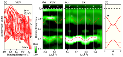
Figure 5(a) shows energy distribution curves (EDCs) measured with synchrotron radiation in the VUV region at the normal-emission set up, reproduced from Fig. 1(b). One can recognize that the energy location of the -band bottom shows a systematic variation as a function of and such variation is also visualized in the second-derivative intensity plot in Fig. 5(b). From the periodicity of band dispersion together with the normal-emission ARPES data obtained with SX photons [Fig. 5(c)], we have estimated the inner-potential value to be = 10.0 eV.
I.3 SOC-induced gap opening on a Dirac band
Figures 6(a) and 6(b) show the magnified view of the APRES intensity around the Dirac gap and the corresponding EDCs, respectively, in which the gapped nature of Dirac cones is clearly visible.
I.4 Hump structure in the CDW phase
In Fig. 7(a), we reproduce two EDCs from Fig. 2(c) in the main text; the magenta and green curves were recorded at 20 K at = 0 and , respectively. The peak position of the magenta curve (70 meV) is shifted toward higher binding energy compared with that of the green curve (40 meV), indicative of a CDW-gap opening at = 0 (note that the CDW gap at = is not visible due to the limited resolution of synchrotron-based ARPES). To confirm that the observed peak-energy shift is not due to noise, we have evaluated the noise level of the spectrum. We have estimated the standard deviation () in the linear fit to a feature-less energy region (black line) and obtained the noise level of 2 (see light blue lines; note that the linear fit would give the upper limit for the noise level because the inclusion of additional parameters commonly gives a better fit). It is remarked here that the peak height of the magenta curve [roughly 10, see Fig. 7(a)], as defined by the difference in the spectral intensity at 70 meV and 40 meV, is more than twice larger than the noise level (4). This demonstrates that the observed peak-energy shift is not an artifact due to noise, but reflects the CDW-gap opening. To further corroborate the CDW-gap opening, we plot in Fig. 7(b) the EDCs measured at 20 K along a k cut including the point [blue arrow in the inset to Fig. 7(a)]. One can see that the band (blue shade) dispersing from the high binding energy side reaches the binding energy of 70 meV at (magenta curve) and then almost flattens, in agreement with the CDW-gap opening in the band.
I.5 -broadening effect
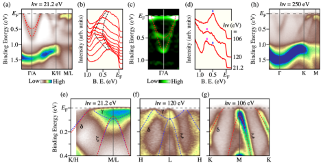
Figure 8(a) shows the ARPES intensity measured along the KM/AHL cut with the He-I photons ( = 21.2 eV). One can identify electron-like band ( band) centered at the /A point. A closer look at the EDCs around the /A point reveals that the band consists of two branches each bottomed at of 0.5 and 0.75 eV [see Fig. 8(b); also see the second-derivative intensity around the /A point in Figs. 8(c)]. These branches are attributed to the band at the = 0 (KM) plane and at the = (AHL) plane, respectively, as supported by the observation of the -band bottom at 0.5 eV at = 0 and 0.75 eV at = [Fig. 8(d); also see Figs. 1(c) and 1(d)] which agrees well with the energy position of the two peaks at = 21.2 eV. Considering short photoelectron escape depth (5-10 Å) of 21.2-eV photons and a resultant large broadening effect, the ARPES data reflect the photoelectron signal averaged over a wide area in the bulk BZ so that the band structures at = 0 and planes which have a large contribution to the density of states are simultaneously observed. Such a broadening effect is also seen around the Brillouin-zone corner. Namely, the band dispersions observed along the MK/LH cut with 21.2-eV photons can be explained by a simultaneous observation of the bulk bands at = 0 and [see Figs. 8(e)-8(g)]. It is noted that overall band dispersions in a wide energy range and their ARPES-intensity distributions obtained with He-I photons [Fig. 8(a)] also agree with those for the bulk bands observed with SX photons [Fig. 8(h)] except for the appearance of the second -band branch, supporting the bulk origin of the observed bands. Here, we briefly comment on the amount of the dispersion. Since the -band bottom is located at 0.5 eV and 0.75 eV at = 0 and , respectively, the total dispersion is 0.25 eV in the experiment. This is smaller than the calculated value of 0.4 eV, suggesting that the dispersion is overestimated in the calculation.
I.6
I.7 Full data set for the CDW-gap measurements
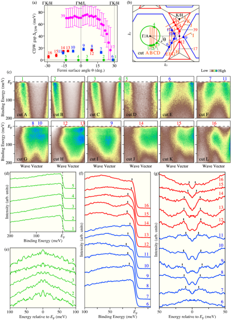
Figure 9(a) shows the gap plot reproduced from Fig. 3(e) but additionally includes the numbering of the k points at which the gap size has been estimated [see Fig. 9(b)]. Figure 9(c) shows the ARPES intensity plots at = 10 K along various k cuts with different Fermi surface angles () [orange lines A-L in Fig. 9(b)]. One can see a general trend that the band dispersion around the M point ( = 0∘) is flattened by an opening of a large CDW gap (e.g, cuts G, H, and J), while a relatively steep dispersion is retained around the K cut ( = 30∘; e.g., E, F, and L) due to a small CDW gap. Figures 9(d)-9(g) display EDCs measured at various points indicated by red triangles in Fig. 9(c), for the band [Fig. 9(d)] and the Dirac band [Fig. 9(f)], as well as the corresponding symmetrized EDCs [Figs. 9(e) and 9(g) for the and Dirac band, respectively]. For the band, one can recognize the absence of a clear gap opening irrespective of . For the Dirac band, blue curves in Figs. 9(e) and 9(f) were obtained on the large hexagonal Fermi surface centered at the /A point, whereas red ones were obtained on the triangular Fermi surface centered at the K/H point. The gap size estimated on these Fermi surfaces is almost the same in magnitude and shows a similar anisotropy; it shows the maximum of 16-18 meV along the M/AL line ( = 0∘), while it shows the minimum of 0-5 meV along the K/AH line ( = 30∘). EDCs for the saddle-point band are displayed in Fig. 2(g) of the main text.