Interplay of charge noise and coupling to phonons in adiabatic electron transfer between quantum dots
Abstract
Long-distance transfer of quantum information in architectures based on quantum dot spin qubits will be necessary for their scalability. One way of achieving it is to simply move the electron between two quantum registers. Precise control over the electron shuttling through a chain of tunnel-coupled quantum dots is possible when interdot energy detunings are changed adiabatically. Deterministic character of shuttling is however endangered by coupling of the transferred electron to thermal reservoirs: sources of fluctuations of electric fields, and lattice vibrations. We theoretically analyse how the electron transfer between two quantum dots is affected by electron-phonon scattering, and interaction with sources of and Johnson charge noise in both detuning and tunnel coupling. The electron-phonon scattering turns out to be irrelevant in Si quantum dots, while a competition between the effects of charge noise and Landau-Zener effect leads to an existence of optimal detuning sweep rate, at which probability of leaving the electron behind is minimal. In GaAs quantum dots, on the other hand, coupling to phonons is strong enough to make the phonon-assisted processes of interdot transfer dominate over influence of charge noise. The probability of leaving the electron behind depends then monotonically on detuning sweep rate, and values much smaller than in silicon can be obtained for slow sweeps. However, after taking into account limitations on transfer time imposed by need for preservation of electron’s spin coherence, minimal probabilities of leaving the electron behind in both GaAs- and Si-based double quantum dots turn out to be of the same order of magnitude. Bringing them down below requires temperatures mK and tunnel couplings above eV.
I Introduction
In quantum computing architectures based on voltage-controlled quantum dots (QDs), developed in GaAs/AlGaAs [1, 2, 3], Si/SiGe [4, 5], and silicon MOS [6, 7, 8, 9] structures, scalability will be possible only if quantum information is transferred between few-qubit registers, separated by distances much larger than the typical QD size. This is caused by short-distance character of exchange interaction needed for two-qubit gates, and spatial extent of wiring needed for controlled application of voltages to the gates defining the dots, which together put limits on density of a qubit array [10]. Coupling of electron spins to microwave photons is a possible mean of coherent coupling of spin qubits in GaAs [11] and silicon [12, 13, 14, 15]. A conceptually simpler alternative, which has been recently pursued in experiments [16, 17, 18, 19, 20, 21, 22, 23, 24, 25, 26, 27, 28], is to simply transfer an electron spin qubit over a large (at least a few micrometer) distance.
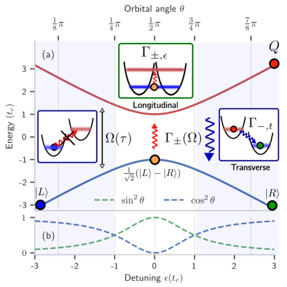
We focus here on electron transfer along a chain of tunnel-coupled QDs [22, 23, 24, 25, 26, 27, 28]. The shuttling is then caused by controlled tilting of energy levels of neighboring QDs that makes an electron move from one dot to the other. The basic step in such a process is single electron transfer between two tunnel-coupled QDs. In a simplified situation, in which we neglect spin and valley (in case of Si) degrees of freedom of the electron, the basic physics is captured by the Hamiltonian acting in a two-dimensional Hilbert space spanned by states, corresponding to electron localized in a local ground states of energy in left (right) dot:
| (1) |
where is the so-called interdot detuning of energy, is the tunnel coupling between the QDs, , and . For the lowest energy state is localized in the dot, and this is the state that we take as an initial one in all the considerations below. For the lowest-energy state is localized in the dot, and one of course expects that for very slow change of from negative to positive values, the evolution will be adiabatic and the system will end up in this state. For a linear sweep, , where is the rate of change of detuning, and constant , we are dealing with classical Landau-Zener model [29], for which the probability of having the electron in an exited state for (i.e. leaving the electron behind in the L dot) is given by
| (2) |
so that a near-perfect adiabatic transfer occurs when , i.e. when the sweep rate is low.
Changing the interdot detunings slowly is thus an obvious way to perform an on-demand deterministic transfer of an electron spin qubit. Of course, the total shuttling time should be much shorter than the spin coherence time of a moving electron, and according to Eq. (2) this requirement will put a lower bound on values of characterizing the chain of QDs. However, another issue needs to be addressed before we can claim to have a realistic estimate of sweep rate giving the smallest possible probability of error in transfer between a pair of dots. Electrons are affected by charge noise unavoidable in semiconductor nanostructures, and coupled to lattice vibrations. As we show in this paper, interactions with sources of electric field noise and phonons in realistic Si- and GaAs-based structures are dominating the physics of charge transfer in a wide range of sweep rates, with nonadiabatic effects described by Landau-Zener theory being relevant only for very fast sweeps.
Since our focus here is on open system character of an electron tunneling between two quantum dots, we use the above-described simplest possible two-level model of the closed system. Taking into account the spin degree of freedom and spin-orbit cupling that affects its dynamics during the electron motion in GaAs [30] (and to a smaller extent in silicon [30, 31]), and then a valley degree of freedom in Si [32, 33, 34], leads to 4- or 8-level models with multiple anticrossings of states [30, 35, 36, 37, 38, 39, 31, 40, 41]. The two-level model used here exhibits a simpler behavior in closed system case, and using it will typically lead to an underestimation of unwanted effects due to not-slow-enough sweeps (for a closed system), and coupling to environment (for an open system). The results given in this paper consequently correspond to the best-case scenario for given and assumed magnitudes of charge noise and temperature.
The physics of Landau-Zener effect in presence of coupling to environment has obviously been a subject of multiple works. Dissipative adiabatic evolution affected by coupling to bosonic baths having Ohmic spectrum was most often considered [42, 43, 44, 45, 46, 47]. It is known [48, 49] that coupling to zero-temperature bath suppresses the final occupation of the higher-energy state (“the electron being left behind in the initial dot” in the physical scenario of interest here), while at finite temperature this occupation can be enhanced [50, 51, 52, 43, 53]. Such effects of coupling to low-temperature reservoirs were discussed in many physical contexts [54, 42, 55]. Stochastic modifications of LZ parameters were also considered [56, 57, 58], including fast classical fluctuations [59] and noise characterized by non-trivial spectral density [60, 61, 62, 63, 39], including 1/f type noise, the tail of which also resulted in incoherent transitions between the states [64, 39, 65]. In this paper we focus on quantum dots based on silicon and GaAs, and employ realistic models of charge noise (having both Johnson/Ohmic and type spectra, and coupling to both and ), and phonon interaction with an electron confined in a double quantum dot. We use the Adiabatic Master Equation [66, 53, 42], in which the influence of the environment (actually a few distinct reservoirs in the case discussed here) is modeled with energy-dependent rates of transitions between instantaneous eigenstates of the slowly changing Hamiltonian of the system. For negligible probability of coherent Landau-Zener excitation, this approached reduces to a simple differential rate equation [67, 68]), which we solve in a way analogous to the one described in [53].
During the detuning sweep, the energy gap between eigenstates of instantaneous Hamiltonian varies between eV and largest value of meV. With temperatures in experiments typically around mK, corresponding to thermal energy of eV, we should expect a nontrivial role of temperature dependence of rates of energy absorption and emission by the reservoirs. Note that in our previous work [39] we have focused on influence of classical (i.e. high-temperature) charge noise on electron transfer. Here we address the situation of lower temperatures/larger tunnel couplings, taking into account the quantum limit [69] of both noise from two-level fluctuators present in the nanostructure, and Johnson noise from reservoirs of free electrons, while furthermore considering the coupling of the moving electron to phonons. Coupling to all these thermal reservoirs gives transition rates, for transfer of energy from/to the environment, that nontrivially depend on . The detailed balance between them, which reads , has the following general consequence for the dynamics of the system. With the system initially in ground state, transitions into an excited are exponentially suppressed for large negative detunings, and they start to become increasingly efficient as we approach the anticrossing of levels, at which the gap is minimal and equal to . This effect of enhancement of excitation rate at the anticrossing is additionally strengthened in the considered system by the fact that an electron delocalized between the two dots is more susceptible to both charge noise and interaction with phonons (as the transitions between states localized in each dot that govern the dynamics in far-detuned regimes are suppressed by small overlap of wavefunctions). The finite occupation of the “wrong” dot generated during passing through region can then be diminished (“healed” in the terminology used below) by processes of energy emission into the reservoirs that dominate over processes of energy absorption by them when . Arriving at the final result of interplay between environment-induced excitation near the anticrossing, and the subsequent energy relaxation (the environment-assisted dissipative tunneling into the “correct” final state), requires consideration of realistic coupling to all the reservoirs at temperatures and sweep rates relevant for experiments in quantum dots. Such a careful consideration is the goal of this paper.
Our key qualitative result concerning application to realistic quantum dots, is that in Si-based structures (both Si/SiGe and SiMOS) the dominant process disturbing the adiabatic evolution close to anticrossing of levels is due to charge noise (with coupling to phonons giving transition rates order of magnitude smaller than those estimated for charge noise), and the finite probability of leaving the electron behind is subsequently diminished by relaxation processes due to charge noise and phonons that occur at large detunings only when the transfer is very slow. On the other hand, in GaAs/AlGaAs structures the piezoelectric coupling to phonons dominates over coupling to charge noise over a wide range of detunings, and consequently the processes involving energy exchange between the transferred electron and lattice vibrations dominate the physics of the problem. The longer the charge transfer takes, the more time the system spends in far-detuned regime in which the energy gap exceeds thermal energy, and the closer it gets to a thermalized state characterized by small occupation of higher-energy level, i.e. of the electron being in the wrong dot. Phonons thus help in maintaining a deterministic character of the charge transfer. These conclusions are quite robust against modifications of parameters of high-frequency properties of Johnson and type charge noises considered here.
The article is organized in the following way, in Sec. II we set up the problem for the closed system and discuss the adiabatic condition for its dynamics, introduce the Adiabatic Master Equation as an approach to open system dynamics, and discuss a few physically transparent (and, as we show later, relevant for the case of electron transfer in silicon- and GaAs-based quantum dots) approximate solutions of this equation. In Section III we calculate the detuning-dependent transition rates between instantaneous eigenstates of the two-level Hamiltonian. We perform calculations for coupling to phonons, and finite-temperature environments that cause charge noise of both Johnson and type in detuning and tunnel coupling. We give there a discussion of expected amplitude of noise at GHz frequencies relevant for transitions during electron transfer in realistic GaAs- and silicon-based quantum dots. Finally, in Section IV we use these rates to calculate the dynamics of the electron driven adiabatically through an anticrossing of levels associated with the two dots, and show a qualitative difference between resulting probability of “leaving the electron behind” between GaAs- and silicon-based quantum dots. In the last Section we discuss some of the implications of these results for experimental efforts aimed at using chains of quantum dots for coherent shuttling of electron spin qubits.
II Model of System’s dynamics
II.1 Adiabatic condition for closed system
We consider two energy levels that in the double quantum dot case correspond to the lowest-energy orbital states localized in each of the two dots, and . In case of silicon QDs we assume that the valley splitting is large enough for us to consider a single anticrossing of two lowest-energy valley-orbital levels. We also neglect the spin degree of freedom - interplay between the nonadiabatic effects in charge transfer and dynamics of the spin of the transferred electron will be discussed elsewhere [70]. We therefore work with the model defined by Hamiltonian from Eq. (1), in which we now assume that and depend on time .
For any value of and tunnel coupling , the Hamiltonian has eigenstates
| (3) |
where . The discussion of nonadiabatic effects due to time-dependence of and , or effects of interaction with the environment, is most transparent if we transform the state of the system into an “adiabatic frame” [71]: instead of working with which fulfills we work with , where a time-dependent unitary operator
| (4) |
transforms the states into the instantaneous eigenstates of : . One can see that for a perfectly adiabatic evolution of the system, for which an initial superposition of eigenstates of at given evolves into the same superposition of eigenstates of at the final time , the transformed state is time-independent. Indeed, the evolution in the adiabatic frame is controlled by
| (5) |
which for the system discussed here reads
| (6) |
where , are Pauli operators in basis of instantaneous eigenstates of the time-dependent Hamiltonian , , and the instantaneous energy splitting is
| (7) |
We assume the electron is initialized in the ground state at large negative detuning , such that the initial state . Due to non-negligible coupling between the adiabatic states during the system’s evolution (i.e. a nonzero term in Eq. (6)), a non-zero occupation of excited state can be generated. When the detuning sweep terminates at large , the occupation of excited state defines the transfer error, i.e. the probability of the electron being left behind in the dot:
| (8) |
The calculation of for an electron coupled to environments relevant for semiconductor-based gated quantum dots is the main goal of this paper.
For constant tunnel coupling , and for we are dealing with the well-known Landau-Zener model [72], in which is given by from Eq. (2). We concentrate here on the adiabatic regime, defined by , which implies , and means that the ratio of “transverse” and “longitudinal” terms in the effective Hamiltonian, Eq. (6), fulfills
| (9) |
This is the adiabatic condition for the dynamics of closed and noise-free system. When it is fulfilled during detuning sweep, the electron remains at all times in the ground state , which means it physically moves from the state initially localized in the left dot , to a final state , located in the right dot.
II.2 Dynamics of an open system
We use here Adiabatic Master Equation (AME) approach [51, 66, 53, 55], in which transitions caused by the environment occur between the instantaneous eigenstates of , which are given by Eqs. (II.1). Our focus on the adiabatic regime (), combined with relatively weak coupling to charge noise (with noise RMS ) and short intrinsic correlation time of phonon bath allow us to use here a Lindbladian form of AME [43, 42], which reads:
| (10) |
where and is the density matrix of the system before switching the description to the “adiabatic” frame, , , and
| (11) |
is the Linbladian associated with operator and time-dependent relaxation/excitation rate . In this approach these rates depend on time though their dependence on the value of instantaneous energy splitting from Eq. (7), i.e. . Below we will use both notations, and , depending on context. In particular, if noise-induced excitations dominate over the Landau-Zener effect due to deterministic time-dependence of , i.e. , the unitary evolution can be safely neglected and Eq. (10) reduces to a simple rate equation
| (12) |
where denotes occupation of the higher energy state at time .
II.3 Approximate solutions
Let us now discuss a few physically motivated approximate solutions for the probability of ending up in the excited state at the end of the sweep , i.e. the probability that the electron remains in the initial dot. We start with a simplest perturbative approach to rate equation (12), assuming . In the lowest order one can write:
| (15) |
As the energy needed for transition from ground to excited state comes from thermal fluctuations of environment, the excitation rate is strongly suppressed at low temperatures, when . At these temperatures the rate of energy relaxation into the environment, , is temperature-independent, as the thermal occupation factor for environmental states of energy is zero, and depends then only on density of environmental states and coupling matrix elements. For all the environments considered in this paper, these dependencies lead to a power-law behavior of the rates, with depending on the transition mechanism and range of , see derivations in the next Section. As we assume the environment to be in thermal equlibrium, the detailed balance condition, which reads , leads to with at low temperatures.
The excitation process takes then place in a narrow range of detunings around the avoided crossing, as very quickly decreases when increases. As for , we neglect in this regime the dependence of and replace it with value for (equivalently: for ), while we keep it in the thermal factor. The integrand in (15) can then be approximated as , and the integration can be done over a range of . In this way we obtain the Single Excitation Approximation Limit (SEAL):
| (16) |
which assumes that at most a single quantum jump from ground to excited state takes place in the avoided crossing region.
The SEAL approximation does not take into account possibility of electron transition in the opposite direction, i.e. from excited to ground state, which would lead to partial recovery of ground state occupation - an effect that we will refer to as a “healing” of excitation that occurred close to the anticrossing. This effect is captured by the factor in Eq. (II.2) with , given in Eq. (14)), evaluated in the low-temperature limit of . The effect of transitions occuring during the part of the sweep when is captured by a Healed Excitation Approximation Limit (HEAL):
| (17) |
The physical picture expected to hold at low is thus the following. A finite is generated due to coupling to a thermal reservoir near the anticrossing, and then processes of emission of energy into this reservoir lead to a diminishing of its final value at the end of the sweep, making the final state of the system closer to the one following from an ideal adiabtic evolution. Such a healing process results in environment-assisted inelastic tunneling into ground state at the end of the driving, see Fig. 1. In Sec. IV we will demonstrate in which regimes of parameters the SEAL/HEAL solutions are applicable for realistic DQD devices.
Note that up to this moment we have not specified any particular form of relaxation/excitation rates , which makes above approximations suitable also for other systems described in terms of the L-Z Hamiltonian (1), in the adiabatic limit () and coupled to environment at relatively low-temperature ().
III Transition rates for an adiabatically transferred electron
III.1 General properties
We consider now a transfer of an electron between two quantum dots that is driven by a detuning sweep slow enough to be adiabatic in the closed system limit. After turning on a weak coupling to an environment, the transition rates in the Adiabatic Master Equation (AME) from Eq. (10) are evaluated at given as if the system described by the instantaneous Hamiltonian from Eq. (1), was subjected to an off-diagonal coupling with an environment for a long enough time for Fermi Golden Rule (FGR) calculation to be applicable. Thus the general form of electron-environment coupling in the basis, at given should be expressed in the basis of eigenstates of instantaneous Hamiltonian, , using , which leads to
| (18) |
where and . This means that at every we do the FGR calculation for coupling, where acts in basis of eigenstates of the instantaneous . With the environmental Hamiltonian given by , we calculate then the quantum spectral density for the operator , given by [73, 69]
| (19) |
where is the averaging over the environmental density matrix . The rate of excitation of the system, i.e. a transition that involves taking energy from the environment, is then given by [73, 69]
| (20) |
while the relaxation rate is
| (21) |
For an environment in thermal equilibrium which we consider here, we have and the detailed balance condition, , and thus , is fulfilled.
As the longitudinal and transverse couplings in dots basis are often of different physical origin, we assume , so that the transition rate can be written as , where we introduced
| (22) |
contributions, defined using spectral densities of and operators, and . The coupling that is longitudinal in the basis (the dot basis) appears due to fluctuations of detuning or phonons coupling to the operator . It is most efficient at causing transitions between states when the latter have a molecular-orbital character, i.e. , , , and . On the other hand, the transverse coupling is due to fluctuations of tunnel coupling or phonons coupling to the operator . It leads to transitions of interdot character between the states that correspond to states at and (i.e. and , respectively), see Fig. 7b. Below we will see that for all the considered mechanisms, the transverse processes are weaker than the longitudinal ones, i.e. , so the latter could become relevant only in a very far-detuned regime.
For an electron in a double quantum dot, the relevant mechanisms of transitions between the eigenstates are due to coupling of electron charge to two reservoirs: lattice vibrations (phonons) and sources of fluctuations of electric fields – free electrons in metallic electrodes and ungated regions of semiconductor quantum well being the sources of Johnson noise, and bound charges switching between a discrete number of states being the sources of type noise [74]. Due to their distinct physical origin, we neglect correlations between different transition mechanisms and write the relaxation rate as:
| (23) |
In the above, we separated charge noise contribution into due to tail of 1/f-like noise from two-level fluctuators [65] in the quantum well interface and due to Johnson’s noise caused by wiring in vicinity of quantum dots [75]. As a direct consequence of Eq. (23) the exact formula for leaving electron in the initial dot reads:
| (24) |
where indices stands for phonon, 1/f or Johnson’s mechanisms, while .
Let us discuss now the quantum noise spectra relevant for the two types of reservoirs being the sources of charge noise, and the lattice vibrations.
III.2 Charge noise
The way in which sources of charge noise couple to the electron in a DQD is most easily visible if we consider the high-temperature (or low energy transfer) limit of . The quantum spectral density becomes then symmetric in frequency, (so that ), and it can be identified with a classical power spectral density of a classical stochastic process describing the fluctuations of the electric fields caused by the dynamics of the reservoir. These processes manifest themselves as time-dependent corrections to parameters of : and for detuning and tunnel coupling noise, respectively. As long as the amplitude of the noise is small (), the modification of the instantaneous splitting is negligible. However, time variation of and activates coupling between the eigenstates of the instantaneous Hamiltonian from Eq. (6)), as in the lowest order in and we have
| (25) |
where , and the last approximation relies on assumption to neglect contributions not larger than the noiseless coupling , see Eq. (9). As we neglect correlations between and , we treat the transitions induced by these two noises independently. Taking then into account that the classical spectrum (where denotes now averaging over realizations of noise) is related to the classical spectrum of noise by , and that and , we have
| (26) | ||||
| (27) |
In these equations the arguments can be, of course, replaced by , as the classical spectra are symmetric in frequency. In Appendix A we give an alternative derivation of these results (in the spirit of methods used previously in [39, 61]). We also show there that the AME calculation using these rates agrees very well with direct averaging of evolution due to averaged over realizations of classical noise with experimentally relevant parameters (discussed below in this Section). In this way we check the applicability of AME to the system of interest in this paper in the classical noise/high temperature regime.
Eqs. (26) and (27) connect the rates as given with (classical) spectra of appropriate noise at frequencies. Extension of AME to regime of lower temperatures/higher amounts then to replacing the classical spectra, , by their quantum counterparts, . Let us now discuss the classical and quantum regimes for the two charge noise spectra relevant for semiconductor quantum dots in GHz range ( eV) of energies.
First we consider electric fluctuations from electron gas in metallic gates, the Johnson-Nyquist noise of general form [76, 69, 77]:
| (28) |
where is the inverse of conductance quantum and is the impedance of a noise source, which we model here as an ideal resistor (R) of the impedance given by typical for microwaves . The temperature-dependent part of Eq. (28) reduces to Bose-Einstein distribution for negative frequencies (absorption) and for (stimulated and spontaneous emission). In the GHz frequency range relevant here, Johnson noise from a lossy transmission line discussed in [78] for Si/SiGe quantum dot, gives at most an order of magnitude larger noise power.
Next, we consider -type fluctuations of electric field due to two-level fluctuators (TLFs) localized in the insulating regions of the nanostructure [74]. We focus first on noise in detuning, as there are numerous measurements of spectrum of this noise in DQDs. Due to very high spectral weight at low frequencies such a noise dominates the dephasing of qubits the energy splitting of which depends on electric fields [74, 79]. Here, however, we focus on high (GHz range) positive and negative frequency behavior of that is of character at very low frequencies. The behavior of quantum noise caused by an ensemble of TLFs at such frequencies depends on microscopic details of these fluctuators and the distribution of their parameters, see [65] and references therein.
Here, as in [80], where Si/SiGe charge qubit in a DQD was considered, we take with noise amplitude directly extrapolated from the low-frequency regime, i.e. for positive-frequency quantum spectrum we have
| (29) |
where /s and is a commonly reported classical spectral density at Hz, which at electron temperature of mK in typical Si/SiGe device is given by eV2/Hz [81, 82, 83, 84, 85]. As scaling was observed in experiments on quantum dots [83, 85, 84], we assume here . The negative-frequency quantum spectrum follows from Eq. (29) using the detailed balance condition. It is commonly believed that charge disorder in Si-MOS should have larger amplitude, for example mKeV2/Hz was measured in [86] at mK. However, following [87] and references therein, we assume that the noise amplitude in Si-MOS can be made comparable or even smaller then Si/SiGe [83].
Let us stress that the character of noise generated by an ensemble of TLFs above MHz frequency is not universal, as its amplitude and exponent varies between the DQDs materials and devices. In particular, recent measurements of charge noise in Si/SiGe [88] and Si-MOS [89] showed and scaling up to MHz and MHz respectively, which contrasted with few orders of magnitude weaker amplitude of charge noise at MHz frequencies in some of GaAs singlet-triplet qubits [90, 91]. Additionally, in neither experiment a linear scaling of spectral density with temperature was seen at highest frequencies, and in particular the Si/SiGe case showed only weak dependence on the temperature, confirmed also elsewhere for SiMOS [92, 87], which stood in contrast to GaAs device, where and the spectrum became flat, i.e as was increased [90]. A recent theoretical study [65] of qubit relaxation caused by interaction with an ensemble of TLFs coupled to thermal bath (which create noise at low frequencies) showed that at high positive frequencies (between MHz and GHz, depending on temperature), a crossover first to , and then to a flat or Ohmic spectrum (depending on details of distribution of energy splitting of the TLFs) occurs. One can thus expect that in measurement of high-frequency quantum noise, it is difficult to distinguish the noise caused by TLFs from other sources of electric field fluctuations, as a flat spectrum has been observed already at MHz frequency in SiMOS QD spectroscopy [93]. Let us note that one of the models of distribution of energies of TLFs considered in [65] led to at high frequencies. In light of the above discussion, we use the above model to estimate the relevance of the tail of 1/f noise in silicon-based devices and set eV2/Hz. We will use the same spectrum for GaAs, probably overestimating the noise in this case, but below we will show that for GaAs quantum dots the influence of electron-phonon coupling dominates over that of charge noise having even such a large amplitude.
For the charge noise in tunnel coupling, we assume that it is uncorrelated with the noise in detuning, as the two are caused by TLFs from distinct spatial regions. We parametrize the ratio of rms of fluctuations of the noise in and by , with its value motivated by semiconductor quantum dots experiments [94, 95, 90, 88], and typical values of level arm used to control the electronic gates during shuttling [25]. We conclude this section by giving the explicit forms of longitudinal and transverse contributions to relaxation rates due to charge noise
| (30) | ||||
| (31) |
which are applicable for both and Johnson noise. The corresponding excitation rates are obtained via detailed balance condition .
III.3 Electron-phonon interaction
In semiconductors, another mechanism responsible for transitions between the states is associated with energy exchange between the electron and lattice vibrations. Phonons are assumed to be in thermal equilibrium, with their free Hamiltonian given by , where and represents phonon polarizations and wavevector respectively. The electron-phonon interaction is given by [96]:
| (32) |
in which denotes crystal density, the crystal volume, and is the speed of -polarized phonons. The coupling stands for piezoelectric () and deformation potential (), evaluated for transverse () and longitudinal () polarizations of phonons:
| (33) |
where is piezoelectric constant, while , are dilatation and shear deformation potentials respectively. In GaAs and Si the coupling to phonons takes a very different form, namely Si lacks the dominant in the GaAs piezoelectric coupling [97], while the opposite is true for shear deformation potential since .
We evaluate the matrix elements of interaction from Eq. (32) in the two-dimensional space spanned by states (see Appendix B for details), obtain the form of coupling discussed in Sec. III.1, and arrive at quantum spectra associated with longitudinal () and transverse () couplings to phonons:
| (34) |
where the matrix elements read , and , while the temperature-dependent term reduces to Bose-Einstein distribution for (absorption) and to for (emission). The transition rates are given by
| (35) | ||||
| (36) |
For further calculation we need to specify a model of wavefunctions localized in the uncoupled dots. We assume that they are separable and Gaussian:
| (37) |
where the full width at half maximum (FWHM) of electron wavefunction, which defines dots diameter, is given by in planar, and in the growth direction of structure, while the gives the distance between the dots. Next we use Hund-Mulliken approximation [98, 99], to generate a set of orthogonal states in DQDs system that fulfill , which can be done by setting:
| (38) |
where .
As the energy quanta exchanged between the electron and the lattice are meV, we take into acocunt only the acoustic phonons with . The relaxation rates due to electronphonon interaction are then given by:
| (39) | ||||
| (40) |
where the integration over solid angle of resonant wavevector , with length was denoted by , while the form factors read:
| (41) |
The common term is the Fourier transform of the electron wavefunction, while the main difference between the longitudinal and transverse relaxation is the overlap of bare dots wavefunctions, which makes the transverse relaxation mechanism orders of magnitude weaker, i.e. , unless detuning is so large that is close enough to for term in Eq. (35) suppresses to the degree that is becomes smaller than .
| Quantity | Symbol | Values |
|---|---|---|
| Tunnel coupling | eV | |
| Effective electron temperature | mK | |
| Detuning sweep rate | eV/ns | |
| Initial detuning | eV | |
| Final detuning | eV | |
| Time of detuning sweep | ns | |
| Transverse/longitudinal noise ratio | ||
| Resistance of noisy resistor (Johnson noise) | ||
| 1/f noise amplitude at K | K | |
| Dots separation | nm (GaAs), nm (SiGe), nm (Si-MOS) | |
| Spread of electron wavefunction in XY plane | nm (GaAs), nm (Si/SiGe, Si-MOS) | |
| Width of quantum well | nm (GaAs),nm (Si/SiGe, Si-MOS) |

As the size of quantum dot in planar direction is larger then size in the direction, , its value can be extracted from splitting between the ground and first excited dot state , i.e. . In Si at meV an estimate of nm is consistent with reported values of nm [100], nm [82] in Si/SiGe and nm [101], nm [86] in Si-MOS. The GaAs dots are typically larger (nm [102], nm [103]), mostly due to smaller effective mass, i.e. . The typically reported values of nm [102] in GaAs are also larger than those in Si/SiGe, nm [104], nm [82]. We assume here the extent of electron’s wavefunction in the direction in Si-MOS is similar to that in Si/SiGe, and for both we take it as nm. Finally, smaller dots allow for decreasing the distance between the sites from typical for GaAs nm [102], nm [103] to Si/SiGe values of nm [5], to Si-MOS nm [5]. The distances between the dots are correlated with reported values of , the largest of which are achieved in SiMOS structures, with examples of eV and eV for dots separated by nm [28] and nm [101] respectively. However, recently eV was achieved in Si/SiGe across an array of quantum dots with nm and nm [25]. In GaAs, tunnel coupling of eV was measured in an array of eight quantum dots with nm [2] for array of 8 QDs. Representative parameters for each nanostructure that we will use in subsequent calculations are given in Tab.1.
We now evaluate numerical values of relaxation rates from Eqs. (39) and(40) for above-discussed parameters of “typical” GaAs, Si/SiGe and Si-MOS double quantum dots given in table 1, In Fig. 2 we plot zero-temperature electron relaxation rate due to scattering with phonons, , as a function of detuning (let us recall that ) for three values of tunnel coupling, eV. It is clear that the scattering of a single electron in a DQD in each of considered nanostructures is dominated by a different mechanisms. In polar GaAs, the piezoelectric coupling dominates over the deformation potential one, with the fastest relaxation at low detuning, where the transitions occur between molecular-orbital type states. The relaxation rate, for the energies below shows oscillatory behaviour due to term, see Eq. (III.3). For larger detunings, when the energy transfer , the relaxation rate decreases as its mostly longitudinal character that makes it , is combined with phonon spectral density and piezoelectric coupling , to produce an overall scaling in the far detuned regime , until eV when phonon bottleneck effects start to become strongly viisble. On the other hand, in Si/SiGe a weaker deformation potential scattering gives that first increases with , and then becomes suppressed by phonon bottleneck effect at large detunings. The relaxation time falls below 100 ns for eV only for the largest considered eV. Finally, in Si-MOS the smaller interdot distance makes the transverse relaxation more efficient. Due to its scaling up to phonon bottleneck energy of about meV, it becomes the dominant process at larger detunings. Such a transverse relaxation rate weakly depends on tunnel coupling (note the presence of single blue lines in Fig. 3, and requires overlap between wavefunctions of L/R dots, which is not large enough in the other nanostructures: might be relevant in GaAs only at highest detunings, see Fig. 3a, and the transverse process never becomes of similar order of magnitude as the longitudinal one in the considered Si/SiGe structures.
III.4 Comparison of the transition rates
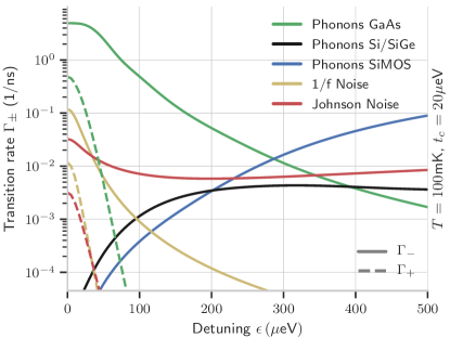
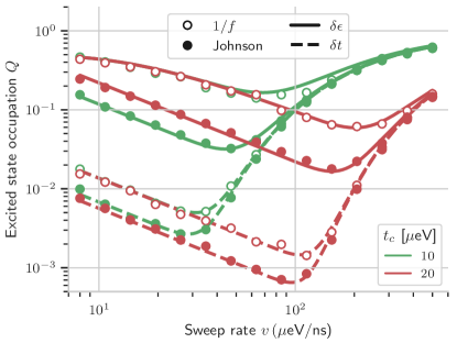
Let us know use the results of the previous Sections and compare the relative importance of various types of environments on the discussed DQD structures. In Fig. 3 we plot the relaxation rate (the excitation rate ) with solid (dashed) lines as functions of detuning for all the considered mechanisms using the above-discussed representative parameters for GaAs, Si/SiGe, and SiMOS structures, and temperature mK and tunnel coupling eV. As expected from discussion in Sec. II.3, the excitation rates are the largest at the anticrossing, and they become suppressed exponentially with increasing above . In that regime the relaxation overwhelmingly dominates over excitation, but the dynamics of the electron will depend on the value of total : the electron tranfer error will depend on the ratio of timescale of environment-assisted inelastic tunneling between the dots in the far-detuned regime, , and the duration of the detuning sweep. Note that for eV the requirement of means eV/ns, so the total time of detuning sweep over a meV range is ns. This will give a ballpark estimate what timescales we should compare to.
In GaAs the coupling to phonons (the green line in Fig. 3 dominates the relaxation, with influence of Johnson noise possibly becoming dominant at highest considered detunings. As discussed above, for most of the considered range of , so for the healing of excitation to be significant the time spent at moderate detunings, up to about 200 eV (see Fig. 3), has to be larger than average relaxation time in this range, ns.
The situation is more complex in Si nanostructures. For parameters of Si/SiGe DQDs it is the Johnson noise - red line in Fig. 3 - that dominates (more visibly at lower ) over the relaxation due to deformation potential coupling to phonons (the black line in Fig. 3). The detuning dependence of this process is rather weak. When (in Fig. 3 we have ), the Johnson noise from resistor gives for stronger longitudinal process, and and in case of weaker transverse one. For their assumed ratio, the relaxation the rates become equal at , which means slowly decreases as up to eV, and then it starts to slowly increase with . The relaxation time for the assumed amplitude of Johnson noise is ns in the relevant detuning range.
Finally, for SiMOS the smaller interdot distance assumed for this architecture makes the dominant relaxation process at large detunings: as show in Fig. 3 this relaxation channel dominates over the one due to Johnson noise for eV. The relaxation times at large detunings approach ns, so phonon-assisted interdot tunneling might be an efficient mechanism of healing of charge noise-induced excitation that occurred close to the anticrossing in SiMOS.
The other mechanisms only weakly contribute to relaxation, as longitudinal 1/f noise relaxation rate is strongly attenuated with increasing detuning, as at , while small overall strength and weak detuning dependence of longitudinal phonon processes in Si/SiGe, , produces relaxation times above ns only approaching the order of magnitude of contribution of Johnson noise around eV.
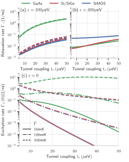
Let us now discuss the tunnel coupling and temperature dependence of the total rate at , and of the total rate at moderate and high detunigs, and eV, respectively. The relaxation rates at moderate detuning have a common dependence on inherited from the tunneling dependence of the dominant there longitudinal process, i.e. . This is not the case at larger detuning, where transverse processes that are weakly dependent on can dominate. Similarly for considered here , temperature dependence of relaxation is very weak. We illustrate both statements in Fig. 4a and 4b where we plot relaxation rates at eV as a function of tunnel coupling. As it can be seen difference between Si/SiGe and SiMOS is visible at large detuning where for small tunnel couplings interdot phonons provide order of magnitude faster relaxation rate in the latter.
In Fig. 4c we illustrate the relevant excitation rate , computed at the avoided-crossing at mK. In GaAs the only relevant mechanism is the coupling between orbital states provided by the phonons, which has a strong scaling with tunnel coupling as long as eV, wher dependence is provided by the piezoelectric coupling () and the resonance term (). As a result, at smaller temperatures, excitation rate in GaAs shows a non-monotonic behaviour as a function of tunnel coupling. In Si, the excitation at is caused only by charge noise, and hence for amplitude of this noise used here for both Si/SiGe and SiMOS, it results in the same rate, in which contributions from and are combined. The latter becomes more relevant at larger , for which however the overall charge noise is attenuated due to exponential factor, as it can be seen in Fig. 4c by a decrease of excitation rate in Si.
IV Probability of leaving the electron behind
Let us use now the above-derived transition rates to calculate the central quantity of this paper – occupation of higher energy state after detuning sweep , i.e. the probability of leaving the electron in the initial dot.
.
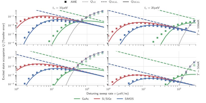
We assume the relevant part of detuning sweep starts and terminates at eV, since at the dots become uncoupled, i.e. the approximation of constant breaks down [94, 105], and the detuning sweep rate used in an experiment can be increased [25]. In Fig. 5 we compare the results of a numerical solution of Adiabatic Master Equation (AME) from Eq. (10), depicted as squares, against the approximation of single excitation at avoided crossing without relaxation process, from Eq. (15), shown as dashed lines, and the approximation of an excitation followed by relaxation processes only, from Eq. (17), shown as solid lines. The dotted line is the Landau-Zener formula from Eq. (2). In the four panels we show results for combinations of tunnel coupling and temperatures: eV (columns), K (rows). With hollow squares we mark the AME results in the region where and are no longer an upper and a lower bound on , as probability of Landau-Zener transition dominates. We stress that in this region the applicability of AME in secular approximation used here is limited [42, 43], however a correction to the L-Z formula computed using different methods correction is expected to be small for prediminantly longitudinal relaxation [51, 53, 45].
Let us now concentrate on the region in which is dominated by effects related to interaction with the thermal environment, where the AME results are plotted as filled squares. For both Si-based devices in a region of moderate we observe that . This suggests that the value of follows from a finite excitation probability in a limited range of detunings (near the anticrossing), and the occupation of the excited state grows with increased time spent in this region. In agreement with this picture, (dashed line), and the electron undergoes a single transition from ground to excited state in vicinity of the anticrossing. We note such a transition from ground to excited state at in SI-based devices is caused solely by charge noise. As the sweep rate is decreased, an increasing time spent during the electron trasnfer in the far-detuned regime, , allows for a significant recovery of ground state occupation by the relaxation mechanism, which is reflected by a deviation from a SEAL approximation and (solid lines) for smallest sweep rates. The healing effect is stronger for the SiMOS device, due to effective phonon relaxation between the dot-like eigenstates at large detunings. The agreement between the result of evaluation of AME, and the approximation is more visible at lower (higher ), since this agreement is expected to improve as . In contrast, in GaAs device, (plotted in green color) decreases monotonically as the sweep rate gets smaller. This is a consequence of a much stronger coupling to environment (specifically piezoelectric coupling to phonons), which on one hand increases probability of transition from ground to excited state in vicinity of the avoided crossing (dashed line), but on the other hand allows for subsequent relaxation even for not-too-high . As a result there is no region in which , however as long as , i.e. the probability of excitation-relaxation-excitation sequence is relatively low (), the result can be well approximated by taking into account only relaxation processes modifying the excitation generated at the anticrossing, i.e. . Finally, when the electron transfer time is long enough to allow for a second transition from ground to excited state, i.e. when , the HEAL formula gives only a lower bound for results of the AME, as visible at low when comparing the squares and solid lines.
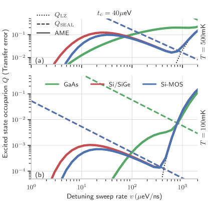
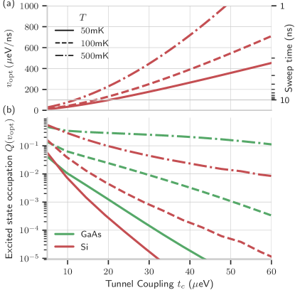
An obvious way to increase the efficiency of charge transfer, or equivalently decrease , would be to bring the result down, as for it gives an upper bound of excited state occupation induced by environmental fluctuations, i.e. in the adiabatic regime where . This can be achieved by lowering the temperature or increasing the tunnel coupling. In Fig. 6 we show a rather optimistic result of probability of leaving the electron in the left dot evaluated for the largest reported in the array of Si/SiGe quantum dots [25], eV. As a reference we compare it to the other materials considered, and plot results for mK, as larger tunnel couplings should in principle allow for working at higher temperatures [106, 107, 108]. We stress that a calculation for mK (not shown) gives for eV/ns. For Si nanostructures the behaviour at higher temperatures is qualitatively similar to than shown in Fig. 5, with a local minimum of , at eV/ns, eV/ns for mK, mK respectively. In GaAs the large value of results in strong coupling between transferred electron and the environment, which at higher temperatures causes flattening of as a function of . This effect can be attributed to reaching thermal equilibrium of around the avoided crossing, followed by slower relaxation at larger .
A local minimum of is thus expected in both Si-based nanostructures considered here. The value of at this minimum can be estimated as the intersection of and , i.e.
| (42) |
the solution to which is expressed in terms of Lambert function [109] as where satisfies equation for . Since typically , the asymptotic form of in the low temperature limit allows to write . As the value of is independent of coupling to environment at larger detunings, the sweep rate which minimizes depends on the charge noise amplitude at , which is assumed here to be the same in Si/SiGe and Si-MOS.
In Fig. 7a we show how in Si varies with for mK. We see that increases as the curve shifts to higher (due to an increase of ), or noise-induced excitations become stronger (here due to an increase of ). Next, in Fig. 7b we use to compare the corresponding transfer error in Si (red) against analogous quantity in GaAs (green), as a function of eV. In the Figure we have put together results of the AME (solid, dashed, dotted dashed lines) for three different temperatures mK. The probability of losing the electron in SiGe appears to be below the value for GaAs for the tunnel couplings apart from the smallest ones of eV, where the corresponding optimal sweep rate (eVns depending on the temperature) is large enough to make the Landau-Zener probability stay above the phonon-induced . Of course, in GaAs can be made lower by using , but there are other factors that are limiting from below in GaAs devices (see discussion in the next Section). Similarly, in Si quantum dots charge transfer can be in principle improved by going to much lower sweep rates ev/ns, however it would make the few-nanosecond transfer impossible as it has been demonstrated by showing the sweep time interval on the right y-axis of Fig. 7a.
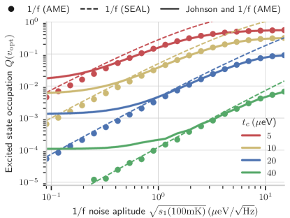
The value of optimal sweep rate and corresponding minimum of transfer error in Si depends on the amplitude of charge noise at frequency corresponding to tunnel coupling (which is in the GHz range), where its influence dominates over that of phonons. We concentrate here on the amplitude of noise, the amplitude of which can vary by at least an order of magnitude between different Si DQD devices. In Fig. 8 we plot a minimal transfer error at typical electron temperature mK as a function of square root of spectral density evaluated at Hz and at mK, which we have previously taken as constant eV/ (see Sec. III.2). We plot the results for range of considered here, and emphasize that noise amplitude can be directly related to excitation rate at with the following formula:
| (43) |
where for brevity and square brackets denoted units in which the quantities should be substituted. The excitation rate obtained using this Equation can be directly used in the SEAL formula, given by Eq. (16), the result of which was illustrated in Fig. 8 using dashed lines. As expected, agrees well with the results of adiabatic Master equation (dots) for relatively small error . Next we analyze transition between and Johnson noise dominated excitations. The latter can be seen in Fig. 8 as a flattening of the solid lines, which represents results of adiabatic master equation with both and Johnson noise, from resistor, contributions. By comparing solid and dashed lines, we conclude that amplitude of noise at which it starts to dominate over Johnson noise becomes larger when the tunnel coupling is increased, which can be deduced from scaling of respective excitation rates, i.e. and for . As the optimal sweep rate is too high to allow for any phonon-mediated suppression of in Si DQDs, the difference between AME and SEAL visible for large noise amplitude is attributed to subsequent relaxation (and further transitions) caused by noise of either large amplitude (eV) or at relatively high temperature (eV, for which ).
V Discussion and summary
We have presented a theory of the dynamics of a system undergoing a Landau-Zener transition in presence of weak transverse and longitudinal couplings to thermal environments: sources of noise of and Johnson type, and a bath of noninteracting bosons, specifically acoustic vibrations of a three-dimensional crystal. Our focus was on the regime in which the deterministic change of parameters of the Hamiltonian is slow enough to neglect the Landau-Zener coherent excitation, and the effectively nonadiabatic character of the evolution can be caused only by interaction with the environment. A general theory based on adiabatic Master equation (AME) was then applied to a case of electron transfer between a pair of voltage-controlled semiconductor quantum dots, for which we took into account realistic parameters for electron-phonon interaction and both Johnson and charge noise. We have calculated transition rates between system’s eigenstates as function of interdot detuning , and used them in AME calculation to obtain the probability of failure of charge transfer between the two dots, , as a function of detuning sweep rate .
When is below the value at which the Landa-Zener transition is activated, only a finite temperature of environment allows for energy absorption necessary for modification of , since otherwise electron would stay in the ground state. This absorption most likely takes place in the vicinity of the anticrossing, where the thermal energy needed for transition is the smallest. A specific feature of the system under consideration is that the dominant coupling to the environment is most effective at the anticrossing, making this effect even stronger. Consequently during the process of electron transfer caused by sweeping the detuning, a finite Q is generated at the anticrossing, when . Then, for larger positive detunings the electron relaxation processes dominate over the excitation processes, and suppression of is expected.
In the considered DQDs there are two possible scenarios. In Si-based dots, coupling to charge noise dominates, and the transition timescale are longer than the typical transfer times, so that the final is very close to the value generated near the anticrossing, which is (proportional to the time spent neart the anticrossing), so it exhibits a dependence on qualitatively opposite to the one for Landau-Zener effect dominating at large . Only at lowest the energy relaxation starts to be efficient at lowering , with this effect being stronger in SiMOS compared to Si/SiGe structures. The competition between the environment-induced excitation and Landau-Zener effect leads then to appearance of optimal , at which is minimal. In GaAs, on the other hand a strong piezoelectric coupling to phonons dominates, transition timescales are shorter than the charge transfer time and consequently many transitions take place, and the final monotonically decreases with decreasing , approaching a value exponentially small in final , reflecting approaching a thermal occupation of the ground state.
The main qualitative theoretical result of the paper, which could also apply to systems other than double quantum dots, is thus that a system described by a Landau-Zener model, when coupled to a thermal environment can realize two possible scenarios: one qualitatively similar to the Landau-Zener effect, but with dependence of on renormalized by environment, and another in which dependence of on is nomonotonic, and there is an optimal sweep rate that minimizes . The main conclusion specific to the considered case of GaAs and Si-based quantum dots is that for mK, in GaAs case can be made smaller than by choosing smaller than eV/ns for eV, while in case of Si having requires eV, and optimal of a few tens of eV/ns. Large tunnel couplings and low temperatures are crucial for having small . In Si-based DQDs there is a possibility of further suppression of by decreasing the level of charge noise at GHz frequencies, corresponding to eV energy splitting at the anticrossing.
A process of a controlled electron transfer between two quantum dots is relevant for ongoing attempts at construction of quantum buses based on chains of many tunnel-coupled dots [23, 25, 28, 40, 70]. Let us now discuss the implications of the results of this paper for prospects of coherent shuttling of electron-based spin qubits across quantum dots. This number of dots in a 1D chain is motivated by requirement of having m distance between few-qubit registers in a realistic architecture of a quantum computer based on gate-controlled QDs [10] and typical interdot separation nm.
When the goal of charge shuttling is an on-demand transfer of qubits, which should be highly coherent, and which are to take part in further coherent manipulations after being moved from one register to another, the deterministic character of the shuttling is necessary. Any randomness in qubit arrival times will complicate the application of subsequent coherent operations involving that qubit. Furthermore, any stochastic component in the duration of the qubit transfer will introduce a random contribution to the phase of the qubit. More in-depth discussion of relationship between the indeterministic character of electron shuttling and spin qubit dephasing will be given in [70]; here it is enough to realize that large probability of electron arriving at the end of -dot chain at a time other than the desired one, will cause major problems in the context of quantum information processing, and we will treat it here as an error probability. Assuming that , the probability of the electron arriving at the end of the chain not at the desired time, i.e the probability of qubit transfer-associated error, is .
Our results for Si-based quantum dots show that for tunnel couplings in eV range, as recently reported in first experimental realizations of electron shuttling over a few dots, achieving will be possible for eV and at mK. Note that a high-fidelity charge transfer between two dots in Si MOS structure was demonstrated experimentally using eV [28], but maintaining such a strong tunnel coupling in a 1D array of quantum dots will be challenging.
In GaAs, on the other hand, can be made much smaller by decreasing the detuning sweep rate , so that the time of interdot transfer becomes longer than ns. This in fact also holds for Si-based dots, only has to be made at least a further order of magnitude smaller. However, for such slow transfers one has to start worrying about well-known mechanisms of spin dephasing that affect the coherence of a static electron localized in a QD. In both the considered materials interaction with nuclei leads to dephasing time of the order or ns for GaAs [110] and a few hundreds of ns for natural Si [111, 112, 113] (and up to tens of microsecond for isotopically purified silicon with about ppm of spinful 29Si [111, 114, 82]). For isotopically purified Si QDs in vicinity of micromagnets, their spatially inhomogeneous magnetic fields together with charge noise lead to s. Let us use now ns ( s) for GaAs and Si. In order to avoid significant spin dephasing during the interdot charge transfer, the time of the latter has to be much shorter than . Assuming that the range of detuning sweep corresponding to the transfer is meV, the sweep rates have to fulfill eV/ns for Si, and eV/ns in GaAs. In Fig. 5 we see that it means that in GaAs this lower bound on severely restricts the possibility of lowering by making the transfer slower, and in fact a tradeoff between amount of spin dephasing and a finite value of due to Landau-Zener effect that dominates the behavior of for eV/ns has to be made. In silicon, the lower bound on is much smaller than , so a local minimum of visible in the Figure is attainable - but the viability of strategy of lowering by using eV/ns depends on the efficiency of electron relaxation due to charge noise and electron-phonon relaxation (compare red and blue lines, corresponding to Si/SiGe and SiMOS in the Figure) and an exact value of . All these observations suggest that from the point of view of coherent transfer of a spin qubit, Si-based quantum dot architectures could have an advantage over GaAs-based ones.
Let us finish by stressing the main message following from our calculations for realistic GaAs and Si-based quantum dots: the dynamics of inter-dot electron transfer is very strongly affected by electron’s interaction with charge noise in Si-based systems and phonons in case of GaAs-based ones. Effects of energy exchange with these environments have to be taken into account to correctly describe the basic physics of electron transfer in the currently available devices. More subtle effects appearing in closed-system description, associated with spin-orbit and valley-orbit (in case of Si) interactions, could become relevant if levels of charge noise are significantly suppressed compared to the currently encountered ones.
Acknowledgements.
We would like to thank Lars Schreiber and Lieven Vandersypen for discussions that motivated us to focus on the problem addressed in the paper, and Piotr Szańkowski for multiple comments on earlier versions of this manuscript. This work has been funded by the National Science Centre (NCN), Poland under QuantERA programme, Grant No. 2017/25/Z/ST3/03044. This project has received funding from the QuantERA Programme under the acronym Si QuBus.Appendix A Correction due to dynamics of classical noise
Here we provide detailed calculations of occupation of excited state in the classical limit, i.e. where the fluctuations of detuning and tunnel coupling can be modeled by stochastic contribution to Hamiltonian (1), i.e.
| (44) |
As pointed out in the main text, in the limit of weak noise corrections comes from noise dynamics, which in the adiabatic frame modifies off-diagonal element of Hamiltonian (6), written explicitly as
| (45) |
where , , and .
A.1 Leading order perturbation theory
We evaluate the leading order excitation probability due to the noisy term. We use first order time-dependent perturbation theory in adiabatic basis , and assuming , we compute leading order the correction to occupation of excited state as , which equals
| (46) |
where denotes classical averaging over noise realizations. The substitution of Eq. (25) into Eq. (46) results in four distinct contributions:
| (47) |
which correspond to auto- or cross-correlation function of respective noise derivative , where or . For assumed here stationary noises, it is convenient to use the Fourier transform of correlation function, which for the noise derrivative can be expressed in terms of power spectral density of noise (PSD) , i.e. [76]. This allows us to write the correction as
| (48) |
in which we introduced filtering function using Eq. (46):
| (49) |
with and .
A.2 Stationary Phase approximation
We evaluate the integral (49) for , in leading order of stationary phase approximation, where we seek for time at which the argument of exponent is stationary, i.e. , from that , which takes place at . Additionally since , the is strictly negative and smaller then . The second derivative, of the phase evaluated at reads . In the leading order, the integral (49) reads:
| (50) | ||||
| (51) |
Now we perform Gaussian integration, , using which integrand terms differ by a phase . Since the result can be written as
| (52) |
First we consider diagonal part () of Eq. (48), in which and . Due to rapidly oscillating nature of both functions, we replace them by average values of and equal 1/2, which leads to:
| (53) |
where the strictly negative value of , reflects absorption of energy quanta. Finally we conclude by showing that cross-correlation is negligibly small. We use the argument that is strictly imaginary, and as a result we have
| (54) |
where the integrand is equivalent to imaginary part of cross-spectrum, and hence vanishes for . Non-trivial imaginary part of cross-spectrum results only from causal relation between , [115], however even in such special case we argue that which due to zero average is expected to be much smaller than auto-correlation contributions. As a result corrections to occupation of excited state due to weak classical noise can be written as:
| (55) |
using which we recovered high frequency limit of [61] where lower bound of the integrals reflects the minimal energy needed for the excitation to occur. Due to the dominant role of longitudinal component we omit here contributions from frequencies below , which are relevant only for transverse noise [61, 60]. In particular corrections from quasi-static noise in tunnel coupling vanishes in assumed here weak noise () and adiabatic () limits [57].
A.3 Transition rates
The first order calculation can be interpreted as a probability of single transition from ground to excited state during adiabatic transfer, and as such can be written as an integral of transition rate , see Eq. (15). An explicit form of can be deduced from Eq. (A.2) as
| (56) |
Finally, we prove that a result obtained by substituting into rate equation Eq. (12), which results in high temperature solution:
| (57) |
is equivalent to an evolution driven by Hamiltonian Eq. (1), averaged over realizations of classical fluctuations of parameters. In Fig. 9 we have separately plotted contributions from detuning noise (solid line), and tunnel coupling noise (dashed line), as a result of noise (hollow dots) and white noise (filled dots). Independently of the considered noise type, in the fast sweep rate limit () we recover the Landau-Zener solution, for which depends on the relation between and only, and thus for sufficiently large the results group according to tunnel couplings eV (green) and eV (red). In the low sweep rate limit, for noise in detuning (solid line, hollow dots) we obtain results from [39], for which ( with ) is independent of . The same applies to noise in tunnel coupling (dashed lines, hollow dots), for which a 10-fold decreased noise amplitude (compared to the case of detuning noise) translates into almost 2 orders of magnitude lower . For the white part of Johnson’s noise, distinction between different is much more visible for noise in detuning (solid lines, filled dots), since larger significantly increases the time spent in vicinity of avoided crossing , during which the longitudinal transitions are most effective. In the case of noise in tunnel coupling the opposite is true, since larger only slightly decreases time spent outside of the avoided crossing region, while .
Appendix B Details of phonon relaxation rate
We now turn to evaluation of zero-temperature phonon relaxation rate in more details. First we show how orbital and interdot phonon-related processes emerge when using the basis of eigenstates of instantaneous Hamiltonian. Next we investigate the elements for Gaussian choice of electron wavefunctions, and discuss the role of harmonic and Hund-Muliken approximation.
B.1 Interdot and orbital processes
We start with the Phonon spectral density, given by Eq. (34), which predicts . We now evaluate the matrix element, by pluging in adiabatic basis given by Eq. (II.1), which results in:
| (58) |
where , and consecutive terms corresponds to interdot (, ) and orbital coupling in dots basis respectively. In absence of large magnetic field in direction, wavefunctions can be assumed real, hence . The exact form of matrix element depends on the assumed form of wavefunctions, i.e. , which will be investigated below.
B.2 Hund-Mulliken approximation
Before invoking concrete form of wavefunction of an electron localized in a QD, let us comment on the so called Hund-Mulliken approximation, in which one uses orthogonalized orbitals built from bare wavefunction of electrons in isolated quantum dots: , with being normalization constant. The parameter is a function of the overlap , with its value given by the orthogonality condition:
| (59) |
from which for . Consistently we concentrate on leading order in or , according to which and we take . Assuming real wavefunction , we substitute the orthogonalized states into Eq. (B.1) from which we obtain:
| (60) |
where in the latter term correction linear in the overlap cancels.
B.3 Harmonic approximation
Finally we substitute concrete form of isolated wavefunctions, and evaluate matrix element . We assume the wavefunction is indepedent in all three directions () and in has a Gaussian shape:
| (61) |
such that for electron wavefunction, FWHM and FWHM. In such case Eq. (B.2) reads:
| (62) |
where we used that in harmonic approximation . Interdot and orbital relaxation are given by real and imaginary part of above matrix element and hence cause relaxation independently.
References
- Hanson et al. [2007] R. Hanson, L. P. Kouwenhoven, J. R. Petta, S. Tarucha, and L. M. K. Vandersypen, Spins in few-electron quantum dots, Rev. Mod. Phys. 79, 1217 (2007).
- Volk et al. [2019] C. Volk, A. M. J. Zwerver, U. Mukhopadhyay, P. T. Eendebak, C. J. van Diepen, J. P. Dehollain, T. Hensgens, T. Fujita, C. Reichl, W. Wegscheider, and L. M. K. Vandersypen, Loading a quantum-dot based “Qubyte” register, npj Quantum Information 5, 29 (2019).
- Kuemmeth and Bluhm [2020] F. Kuemmeth and H. Bluhm, Roadmap for gaas spin qubits, arXiv:2011.13907 (2020).
- Watson et al. [2018] F. Watson, S. G. J. Philips, E. Kawakami, D. R. Ward, P. Scarlino, M. Veldhorst, D. E. Savage, M. G. Lagally, M. Friesen, S. N. Coppersmith, M. A. Eriksson, and L. M. K. Vandersypen, A programmable two-qubit quantum processor in silicon, Nature 555, 633 (2018).
- Lawrie et al. [2020] W. I. L. Lawrie, H. G. J. Eenink, N. W. Hendrickx, J. M. Boter, L. Petit, S. V. Amitonov, M. Lodari, B. Paquelet Wuetz, C. Volk, S. G. J. Philips, G. Droulers, N. Kalhor, F. van Riggelen, D. Brousse, A. Sammak, L. M. K. Vandersypen, G. Scappucci, and M. Veldhorst, Quantum dot arrays in silicon and germanium, Applied Physics Letters 116, 080501 (2020).
- Veldhorst et al. [2017] M. Veldhorst, H. G. Eenink, C. H. Yang, and A. S. Dzurak, Silicon CMOS Architecture for a Spin-Based Quantum Computer, Nature Communications 8, 1766 (2017).
- Huang et al. [2019] W. Huang, C. H. Yang, K. W. Chan, T. Tanttu, B. Hensen, R. C. Leon, M. A. Fogarty, J. C. Hwang, F. E. Hudson, K. M. Itoh, A. Morello, A. Laucht, and A. S. Dzurak, Fidelity Benchmarks for Two-Qubit Gates in Silicon, Nature 569, 532 (2019).
- Gonzalez-Zalba et al. [2020] M. F. Gonzalez-Zalba, S. de Franceschi, E. Charbon, T. Meunier, M. Vinet, and A. S. Dzurak, Scaling silicon-based quantum computing using cmos technology: State-of-the-art, challenges and perspectives, arXiv:2011.11753 (2020).
- Chanrion et al. [2020] E. Chanrion, D. J. Niegemann, B. Bertrand, C. Spence, B. Jadot, J. Li, P.-A. Mortemousque, L. Hutin, R. Maurand, X. Jehl, M. Sanquer, S. De Franceschi, C. B äuerle, F. Balestro, Y.-M. Niquet, M. Vinet, T. Meunier, and M. Urdampilleta, Charge detection in an array of CMOS quantum dots, arXiv:2004.01009 (2020).
- Vandersypen et al. [2017] L. M. K. Vandersypen, H. Bluhm, J. S. Clarke, A. S. Dzurak, R. Ishihara, A. Morello, D. J. Reilly, L. R. Schreiber, and M. Veldhorst, Interfacing Spin Qubits in Quantum Dots and Donors—Hot, Dense, and Coherent, npj Quantum Information 3, 34 (2017).
- Scarlino et al. [2019] P. Scarlino, D. J. van Woerkom, U. C. Mendes, J. V. Koski, A. J. Landig, C. K. Andersen, S. Gasparinetti, C. Reichl, W. Wegscheider, K. Ensslin, T. Ihn, A. Blais, and A. Wallraff, Coherent microwave-photon-mediated coupling between a semiconductor and a superconducting qubit, Nature Communications 10, 3011 (2019).
- Mi et al. [2017] X. Mi, J. V. Cady, D. M. Zajac, P. W. Deelman, and J. R. Petta, Strong Coupling of a Single Electron in Silicon to a Microwave Photon, Science 355, 156 (2017).
- Benito et al. [2017] M. Benito, X. Mi, J. M. Taylor, J. R. Petta, and G. Burkard, Input-output theory for spin-photon coupling in Si double quantum dots, Phys. Rev. B 96, 235434 (2017).
- Mi et al. [2018a] X. Mi, M. Benito, S. Putz, D. M. Zajac, J. M. Taylor, G. Burkard, and J. R. Petta, A Coherent Spin-Photon Interface in Silicon, Nature 555, 599 (2018a).
- Samkharadze et al. [2018] N. Samkharadze, G. Zheng, N. Kalhor, D. Brousse, A. Sammak, U. C. Mendes, A. Blais, G. Scappucci, and L. M. K. Vandersypen, Strong Spin-Photon Coupling in Silicon, Science 359, 1123 (2018).
- Hermelin et al. [2011] S. Hermelin, S. Takada, M. Yamamoto, S. Tarucha, A. D. Wieck, L. Saminadayar, C. Baüerle, and T. Meunier, Electrons surfing on a sound wave as a platform for quantum optics with flying electrons, Nature 477, 435 (2011).
- McNeil et al. [2011] R. P. G. McNeil, M. Kataoka, C. J. B. Ford, C. H. W. Barnes, D. Anderson, G. A. C. Jones, I. Farrer, and D. A. Ritchie, On-demand single-electron transfer between distant quantum dots, Nature 477, 439 (2011).
- Bertrand et al. [2016] B. Bertrand, S. Hermelin, S. Takada, M. Yamamoto, S. Tarucha, A. Ludwig, A. D. Wieck, C. Bäuerle, and T. Meunier, Fast spin information transfer between distant quantum dots using individual electrons, Nature Nanotechnology 11, 672 (2016).
- Takada et al. [2019] S. Takada, H. Edlbauer, H. V. Lepage, J. Wang, P.-A. Mortemousque, G. Georgiou, C. H. W. Barnes, C. J. B. Ford, M. Yuan, P. V. Santos, X. Waintal, A. Ludwig, A. D. Wieck, M. Urdampilleta, T. Meunier, and C. Bäuerle, Sound-driven single-electron transfer in a circuit of coupled quantum rails, Nature Communications 10, 4557 (2019).
- Mortemousque et al. [2021] P.-A. Mortemousque, B. Jadot, E. Chanrion, V. Thiney, C. Bäuerle, A. Ludwig, A. D. Wieck, M. Urdampilleta, and T. Meunier, Enhanced spin coherence while displacing electron in a 2D array of quantum dots, arXiv:2101.05968 (2021).
- Jadot et al. [2020] B. Jadot, P.-A. Mortemousque, E. Chanrion, V. Thiney, A. Ludwig, A. D. Wieck, M. Urdampilleta, C. Bäuerle, and T. Meunier, Distant spin entanglement via fast and coherent electron shuttling, arXiv:2004.02727 (2020).
- Baart et al. [2016] T. A. Baart, M. Shafiei, T. Fujita, C. Reichl, W. Wegscheider, and L. M. K. Vandersypen, Single-Spin CCD, Nature Nanotechnology 11, 330 (2016).
- Fujita et al. [2017] T. Fujita, T. A. Baart, C. Reichl, W. Wegscheider, and L. M. K. Vandersypen, Coherent shuttle of electron-spin states, npj Quantum Information 3, 22 (2017).
- Flentje et al. [2017] H. Flentje, P.-A. Mortemousque, R. Thalineau, A. Ludwig, A. D. Wieck, C. Bäuerle, and T. Meunier, Coherent long-distance displacement of individual electron spins, Nature Communications 8, 501 (2017).
- Mills et al. [2019] A. R. Mills, D. M. Zajac, M. J. Gullans, F. J. Schupp, T. M. Hazard, and J. R. Petta, Shuttling a Single Charge across a One-Dimensional Array of Silicon Quantum Dots, Nature Communications 10, 1063 (2019).
- Nakajima et al. [2018a] T. Nakajima, M. R. Delbecq, T. Otsuka, S. Amaha, J. Yoneda, A. Noiri, K. Takeda, G. Allison, A. Ludwig, A. D. Wieck, X. Hu, F. Nori, and S. Tarucha, Coherent transfer of electron spin correlations assisted by dephasing noise, Nature Communications 9, 2133 (2018a).
- van Diepen et al. [2021] C. J. van Diepen, T.-K. Hsiao, U. Mukhopadhyay, C. Reichl, W. Wegscheider, and L. M. K. Vandersypen, Electron cascade for distant spin readout, Nature Communications 12, 77 (2021).
- [28] J. Yoneda, W. Huang, M. Feng, C. H. Yang, K. W. Chan, T. Tanttu, W. Gilbert, R. C. C. Leon, F. E. Hudson, K. M. Itoh, A. Morello, S. D. Bartlett, A. Laucht, A. Saraiva, and A. S. Dzurak, Coherent spin qubit transport in silicon, arXiv:2008.04020 .
- Shevchenko et al. [2010a] S. N. Shevchenko, S. Ashhab, and F. Nori, Landau-Zener-Stückelberg Interferometry, Phys. Rep. 492, 1 (2010a).
- Li et al. [2017] X. Li, E. Barnes, J. P. Kestner, and S. Das Sarma, Intrinsic errors in transporting a single-spin qubit through a double quantum dot, Phys. Rev. A 96, 012309 (2017).
- Ginzel et al. [2020] F. Ginzel, A. R. Mills, J. R. Petta, and G. Burkard, Spin shuttling in a silicon double quantum dot, Phys. Rev. B 102, 195418 (2020).
- Friesen et al. [2007] M. Friesen, S. Chutia, C. Tahan, and S. N. Coppersmith, Valley splitting theory of sige/si/sige quantum wells, Phys. Rev. B 75, 115318 (2007).
- Culcer et al. [2010] D. Culcer, X. Hu, and S. Das Sarma, Interface roughness, valley-orbit coupling, and valley manipulation in quantum dots, Phys. Rev. B 82, 205315 (2010).
- Zwanenburg et al. [2013] F. A. Zwanenburg, A. S. Dzurak, A. Morello, M. Y. Simmons, L. C. L. Hollenberg, G. Klimeck, S. Rogge, S. N. Coppersmith, and M. A. Eriksson, Silicon quantum electronics, Rev. Mod. Phys. 85, 961 (2013).
- Zhao and Hu [2018a] X. Zhao and X. Hu, Toward high-fidelity coherent electron spin transport in a gaas double quantum dot, Sci. Rep. 8, 13968 (2018a).
- Zhao and Hu [2018b] X. Zhao and X. Hu, Coherent electron transport in silicon quantum dots, arXiv:1803.00749 arXiv:1803.00749v1 (2018b).
- Cota and Ulloa [2018] E. Cota and S. E. Ulloa, Spin-orbit interaction and controlled singlet-triplet dynamics in silicon double quantum dots, J. Phys.: Condens. Matter 30, 295301 (2018).
- Shevchenko et al. [2018] S. N. Shevchenko, A. I. Ryzhov, and F. Nori, Low-frequency spectroscopy for quantum multi-level systems, Phys. Rev. B 98, 195434 (2018).
- Krzywda and Cywiński [2020] J. A. Krzywda and L. Cywiński, Adiabatic electron charge transfer between two quantum dots in presence of noise, Phys. Rev. B 101, 035303 (2020).
- Buonacorsi et al. [2020] B. Buonacorsi, B. Shaw, and J. Baugh, Simulated coherent electron shuttling in silicon quantum dots, Phys. Rev. B 102, 125406 (2020).
- Malla et al. [2021] R. K. Malla, V. Y. Chernyak, and N. A. Sinitsyn, Nonadiabatic transitions in Landau-Zener grids: Integrability and semiclassical theory, arXiv:2101.04169 (2021).
- Yamaguchi et al. [2017] M. Yamaguchi, T. Yuge, and T. Ogawa, Markovian quantum master equation beyond adiabatic regime, Phys. Rev. E 95, 012136 (2017).
- Arceci et al. [2017] L. Arceci, S. Barbarino, R. Fazio, and G. E. Santoro, Dissipative Landau-Zener problem and thermally assisted Quantum Annealing, Phys. Rev. B 96, 054301 (2017).
- Leggett et al. [1987] A. J. Leggett, S. Chakravarty, A. T. Dorsey, M. P. A. Fisher, A. Garg, and W. Zwerger, Dynamics of the dissipative two-state system, Rev. Mod. Phys. 59, 1 (1987).
- Javanbakht et al. [2015] S. Javanbakht, P. Nalbach, and M. Thorwart, Dissipative Landau-Zener quantum dynamics with transversal and longitudinal noise, Phys. Rev. A 91, 052103 (2015).
- Huang and Zhao [2018] Z. Huang and Y. Zhao, Dynamics of dissipative Landau-Zener transitions, Phys. Rev. A 97, 013803 (2018).
- Zueco et al. [2008] D. Zueco, P. Hänggi, and S. Kohler, Landau–Zener tunnelling in dissipative circuit QED, New J. Phys. 10, 115012 (2008).
- Saito et al. [2007] K. Saito, M. Wubs, S. Kohler, Y. Kayanuma, and P. Hänggi, Dissipative Landau-Zener transitions of a qubit: Bath-specific and universal behavior, Phys. Rev. B 75, 214308 (2007).
- Wubs et al. [2006] M. Wubs, K. Saito, S. Kohler, P. Hänggi, and Y. Kayanuma, Gauging a Quantum Heat Bath with Dissipative Landau-Zener Transitions, Phys. Rev. Lett. 97, 200404 (2006).
- Ao and Rammer [1991] P. Ao and J. Rammer, Quantum dynamics of a two-state system in a dissipative environment, Phys. Rev. B 43, 5397 (1991).
- Pokrovsky and Sun [2007] V. L. Pokrovsky and D. Sun, Fast quantum noise in the Landau-Zener transition, Phys. Rev. B 76, 024310 (2007).
- Kayanuma and Nakayama [1998] Y. Kayanuma and H. Nakayama, Nonadiabatic Transition at a Level Crossing with Dissipation, Phys. Rev. B 57, 13099 (1998).
- Nalbach [2014] P. Nalbach, Adiabatic-Markovian bath dynamics at avoided crossings, Phys. Rev. A 90, 042112 (2014).
- Benseny and Mølmer [2020] A. Benseny and K. Mølmer, All’s well that ends well: The unexpectedly good performance of adiabatic passage, arXiv:2010.05093 (2020).
- Chen and Lidar [2020] H. Chen and D. A. Lidar, Why and When Pausing is Beneficial in Quantum Annealing, Phys. Rev. Appl. 14, 014100 (2020).
- Kayanuma [1984] Y. Kayanuma, Nonadiabatic Transitions in Level Crossing with Energy Fluctuation. I. Analytical Investigations, Journal of the Physical Society of Japan 53, 108 (1984).
- Kayanuma [1985] Y. Kayanuma, Stochastic Theory for Nonadiabatic Level Crossing with Fluctuating Off-Diagonal Coupling, Journal of the Physical Society of Japan 54, 2037 (1985).
- Dodin et al. [2014] A. Dodin, S. Garmon, L. Simine, and D. Segal, Landau-Zener transitions mediated by an environment: Population transfer and energy dissipation, J. Chem. Phys. 140, 124709 (2014).
- Pokrovsky and Sinitsyn [2003] V. L. Pokrovsky and N. A. Sinitsyn, Fast noise in the Landau-Zener theory, Phys. Rev. B 67, 144303 (2003).
- Luo and Raikh [2017] Z. X. Luo and M. E. Raikh, Landau-Zener transition driven by slow noise, Phys. Rev. B 95, 10.1103/PhysRevB.95.064305 (2017).
- Malla et al. [2017] R. K. Malla, E. G. Mishchenko, and M. E. Raikh, Suppression of the Landau-Zener Transition Probability by Weak Classical Noise, Phys. Rev. B 96, 075419 (2017).
- Sinitsyn and Prokof’ev [2003] N. A. Sinitsyn and N. Prokof’ev, Nuclear spin bath effects on Landau-Zener transitions in nanomagnets, Phys. Rev. B 67, 134403 (2003).
- Vestgarden et al. [2008] J. I. Vestgarden, J. Bergli, and Y. M. Galperin, Nonlinearly driven Landau-Zener transition with telegraph noise, Phys. Rev. B 77, 014514 (2008).
- Amin and Averin [2008] M. H. S. Amin and D. V. Averin, Macroscopic Resonant Tunneling in the Presence of Low Frequency Noise, Phys. Rev. Lett. 100, 197001 (2008).
- You et al. [2021] X. You, A. A. Clerk, and J. Koch, Positive- and negative-frequency noise from an ensemble of two-level fluctuators, Phys. Rev. Research 3, 013045 (2021).
- Albash et al. [2012] T. Albash, S. Boixo, Daniel A Lidar, and Paolo Zanardi, Quantum adiabatic Markovian master equations, New J. Phys. 14, 123016 (2012).
- Vogelsberger et al. [2006] M. Vogelsberger, D. A. Garanin, and R. Schilling, Butterfly hysteresis curve is a signature of adiabatic Landau-Zener transition, Phys. Rev. B 73, 092412 (2006).
- Haikka and Molmer [2014] P. Haikka and K. Molmer, Dissipative Landau-Zener level crossing subject to continuous measurement: Excitation despite decay, Phys. Rev. A 89, 052114 (2014).
- Clerk et al. [2010] A. A. Clerk, M. H. Devoret, S. M. Girvin, F. Marquardt, and R. J. Schoelkopf, Introduction to quantum noise, measurement, and amplification, Rev. Mod. Phys. 82, 1155 (2010).
- V. Langrock et al. [2021] V. Langrock et al., Proposal of a scalable quantum bus device for coherent mid-range qubit transfer in disordered si/sige/sio2, unpublished (2021).
- Demirplak and Rice [2003] M. Demirplak and S. A. Rice, Adiabatic Population Transfer with Control Fields, J. Phys. Chem. A 107, 9937 (2003).
- Shevchenko et al. [2010b] S. Shevchenko, S. Ashhab, and F. Nori, Landau–Zener–Stückelberg interferometry, Phys. Rep. 492, 1 (2010b).
- Schoelkopf et al. [2003] R. J. Schoelkopf, A. A. Clerk, S. M. Girvin, K. W. Lehnert, and M. H. Devoret, Qubits as spectrometers of quantum noise, in Quantum Noise in Mesoscopic Physics, edited by Y. V. Nazarov (Kluwer, Dordrecht, 2003) pp. 175–203, (cond-mat/0210247).
- Paladino et al. [2014] E. Paladino, Y. M. Galperin, G. Falci, and B. L. Altshuler, noise: Implications for solid-state quantum information, Rev. Mod. Phys. 86, 361 (2014).
- Marquardt and Abalmassov [2005] F. Marquardt and V. A. Abalmassov, Spin relaxation in a quantum dot due to Nyquist noise, Phys. Rev. B 71, 165325 (2005).
- Huang and Hu [2014] P. Huang and X. Hu, Spin Relaxation due to Charge Noise, Phys. Rev. B 89, 195302 (2014).
- Weiss [1999] U. Weiss, Quantum Dissipative Systems (World Scientific, Singapore, 1999).
- Hollmann et al. [2020] A. Hollmann, T. Struck, V. Langrock, A. Schmidbauer, F. Schauer, T. Leonhardt, K. Sawano, H. Riemann, N. V. Abrosimov, D. Bougeard, and L. R. Schreiber, Large, tunable valley splitting and single-spin relaxation mechanisms in a / quantum dot, Phys. Rev. Applied 13, 034068 (2020).
- Szańkowski et al. [2017] P. Szańkowski, G. Ramon, J. Krzywda, D. Kwiatkowski, and Ł. Cywiński, Environmental noise spectroscopy with qubits subjected to dynamical decoupling, Journal of Physics: Condensed Matter 29, 333001 (2017).
- Yang et al. [2019] Y.-C. Yang, S. N. Coppersmith, and M. Friesen, Achieving high-fidelity single-qubit gates in a strongly driven charge qubit with 1/f charge noise, npj Quantum Information 5, 12 (2019).
- Mi et al. [2018b] X. Mi, S. Kohler, and J. R. Petta, Landau-Zener Interferometry of Valley-Orbit States in Si/SiGe Double Quantum Dots, Phys. Rev. B 98, 161404 (2018b).
- Struck et al. [2020] T. Struck, A. Hollmann, F. Schauer, O. Fedorets, A. Schmidbauer, K. Sawano, H. Riemann, N. V. Abrosimov, Ł. Cywiński, D. Bougeard, and L. R. Schreiber, Low-frequency spin qubit energy splitting noise in highly purified 28Si/SiGe, npj Quantum Information 6, 40 (2020).
- Freeman et al. [2016] B. M. Freeman, J. S. Schoenfield, and H. Jiang, Comparison of Low Frequency Charge Noise in Identically Patterned Si/SiO2and Si/SiGe Quantum Dots, Appl. Phys. Lett. 108, 253108 (2016).
- Connors et al. [2019] E. J. Connors, J. J. Nelson, H. Qiao, L. F. Edge, and J. M. Nichol, Low-frequency charge noise in Si/SiGe quantum dots, Phys. Rev. B 100, 165305 (2019).
- Petit et al. [2018] L. Petit, J. M. Boter, H. G. Eenink, G. Droulers, M. L. Tagliaferri, R. Li, D. P. Franke, K. J. Singh, J. S. Clarke, R. N. Schouten, V. V. Dobrovitski, L. M. Vandersypen, and M. Veldhorst, Spin Lifetime and Charge Noise in Hot Silicon Quantum Dot Qubits, Phys. Rev. Lett. 121, 076801 (2018).
- Kim et al. [2019] J.-S. Kim, T. M. Hazard, A. A. Houck, and S. A. Lyon, A low-disorder metal-oxide-silicon double quantum dot, Applied Physics Letters 114, 043501 (2019).
- Kranz et al. [2020] L. Kranz, S. K. Gorman, B. Thorgrimsson, Y. He, D. Keith, J. G. Keizer, and M. Y. Simmons, Exploiting a Single‐Crystal Environment to Minimize the Charge Noise on Qubits in Silicon, Advanced Materials 32, 2003361 (2020).
- Connors et al. [2021] E. J. Connors, J. J. Nelson, and J. M. Nichol, Charge-noise spectroscopy of Si/SiGe quantum dots via dynamically-decoupled exchange oscillations, arXiv:2103.0244 (2021).
- Jock et al. [2021] R. M. Jock, N. T. Jacobson, M. Rudolph, D. R. Ward, M. S. Carroll, and D. R. Luhman, A silicon singlet-triplet qubit driven by spin-valley coupling, arXiv:2102.12068 (2021).
- Dial et al. [2013] O. E. Dial, M. D. Shulman, S. P. Harvey, H. Bluhm, V. Umansky, and A. Yacoby, Charge Noise Spectroscopy Using Coherent Exchange Oscillations in a Singlet-Triplet Qubit, Phys. Rev. Lett. 110, 146804 (2013).
- Cerfontaine et al. [2020] P. Cerfontaine, T. Botzem, J. Ritzmann, S. S. Humpohl, A. Ludwig, D. Schuh, D. Bougeard, A. D. Wieck, and H. Bluhm, Closed-loop control of a GaAs-based singlet-triplet spin qubit with 99.5% gate fidelity and low leakage, Nat. Comm. 11, 4144 (2020).
- Petit et al. [2020a] L. Petit, H. G. J. Eenink, M. Russ, W. I. L. Lawrie, N. W. Hendrickx, S. G. J. Philips, J. S. Clarke, L. M. K. Vandersypen, and M. Veldhorst, Universal quantum logic in hot silicon qubits, Nature 580, 355 (2020a).
- Chan et al. [2018] K. W. Chan, W. Huang, C. H. Yang, J. C. C. Hwang, B. Hensen, T. Tanttu, F. E. Hudson, K. M. Itoh, A. Laucht, A. Morello, and A. S. Dzurak, Assessment of a silicon quantum dot spin qubit environment via noise spectroscopy, Phys. Rev. Appl. 10, 044017 (2018).
- Nakajima et al. [2018b] T. Nakajima, M. R. Delbecq, T. Otsuka, S. Amaha, J. Yoneda, A. Noiri, K. Takeda, G. Allison, A. Ludwig, A. D. Wieck, X. Hu, F. Nori, and S. Tarucha, Coherent transfer of electron spin correlations assisted by dephasing noise, Nat. Comm. 9, 2133 (2018b).
- Shi et al. [2013] Z. Shi, C. B. Simmons, D. R. Ward, J. R. Prance, R. T. Mohr, T. S. Koh, J. K. Gamble, X. Wu, D. E. Savage, M. G. Lagally, M. Friesen, S. N. Coppersmith, and M. A. Eriksson, Coherent quantum oscillations and echo measurements of a Si charge qubit, Phys. Rev. B 88, 075416 (2013).
- Raith et al. [2012] M. Raith, P. Stano, F. Baruffa, and J. Fabian, Theory of spin relaxation in two-electron lateral coupled quantum dots, Phys. Rev. Lett. 108, 246602 (2012).
- Yu and Cardona [2010] P. Y. Yu and M. Cardona, Fundamentals of Semiconductors, Graduate Texts in Physics (Springer Berlin Heidelberg, Berlin, Heidelberg, 2010).
- Burkard et al. [1999] G. Burkard, D. Loss, and D. P. DiVincenzo, Coupled quantum dots as quantum gates, Phys. Rev. B 59, 2070 (1999).
- Li et al. [2010] Q. Li, L. Cywiński, D. Culcer, X. Hu, and S. Das Sarma, Exchange coupling in silicon quantum dots: Theoretical considerations for quantum computation, Phys. Rev. B 81, 085313 (2010).
- Wang and Takahashi [2013] Z.-H. Wang and S. Takahashi, Spin decoherence and electron spin bath noise of a nitrogen-vacancy center in diamond, Phys. Rev. B 87, 115122 (2013).
- Eenink et al. [2019] H. G. J. Eenink, L. Petit, W. I. L. Lawrie, J. S. Clarke, L. M. K. Vandersypen, and M. Veldhorst, Tunable Coupling and Isolation of Single Electrons in Silicon Metal-Oxide-Semiconductor Quantum Dots, Nano Letters 19, 8653 (2019).
- Malinowski et al. [2017] F. K. Malinowski, F. Martins, Ł. Cywiński, M. S. Rudner, P. D. Nissen, S. Fallahi, G. C. Gardner, M. J. Manfra, C. M. Marcus, and F. Kuemmeth, Spectrum of the Nuclear Environment for GaAs Spin Qubits, Phys. Rev. Lett. 118, 177702 (2017).
- Srinivasa et al. [2013] V. Srinivasa, K. C. Nowack, M. Shafiei, L. M. K. Vandersypen, and J. M. Taylor, Simultaneous Spin-Charge Relaxation in Double Quantum Dots, Phys. Rev. Lett. 110, 196803 (2013).
- Wang et al. [2013] K. Wang, C. Payette, Y. Dovzhenko, P. W. Deelman, and J. R. Petta, Charge Relaxation in a Single-Electron Si / SiGe Double Quantum Dot, Phys. Rev. Lett. 111, 046801 (2013).
- Medford et al. [2013] J. Medford, J. Beil, J. M. Taylor, E. I. Rashba, H. Lu, A. C. Gossard, and C. M. Marcus, Quantum-dot-based resonant exchange qubit, Phys. Rev. Lett. 111, 050501 (2013).
- Ono et al. [2019] K. Ono, T. Mori, and S. Moriyama, High-temperature operation of a silicon qubit, Scientific Reports 9, 469 (2019).
- Petit et al. [2020b] L. Petit, M. Russ, H. G. J. Eenink, W. I. L. Lawrie, J. S. Clarke, L. M. K. Vandersypen, and M. Veldhorst, High-fidelity two-qubit gates in silicon above one Kelvin, arXiv:2007.09034 (2020b).
- Yang et al. [2020] C. H. Yang, R. C. C. Leon, J. C. C. Hwang, A. Saraiva, T. Tanttu, W. Huang, J. Camirand Lemyre, K. W. Chan, K. Y. Tan, F. E. Hudson, K. M. Itoh, A. Morello, M. Pioro-Ladrière, A. Laucht, and A. S. Dzurak, Operation of a silicon quantum processor unit cell above one kelvin, Nature 580, 350 (2020).
- Abramowitz and Stegun [1964] M. Abramowitz and I. A. Stegun, Handbook of Mathematical Functions with Formulas, Graphs, and Mathematical Tables, ninth dover printing, tenth gpo printing ed. (Dover, New York City, 1964).
- Chekhovich et al. [2013] E. A. Chekhovich, M. N. Makhonin, A. I. Tartakovskii, A. Yacoby, H. Bluhm, K. C. Nowack, and L. M. K. Vandersypen, Nuclear spin effects in semiconductor quantum dots, Nature Materials 12, 494 (2013).
- Assali et al. [2011] L. V. C. Assali, H. M. Petrilli, R. B. Capaz, B. Koiller, X. Hu, and S. D. Sarma, Hyperfine interactions in silicon quantum dots, Phys. Rev. B 83, 165301 (2011).
- Maune et al. [2012] B. M. Maune, M. G. Borselli, B. Huang, T. D. Ladd, P. W. Deelman, K. S. Holabird, A. A. Kiselev, I. Alvarado-Rodriguez, R. S. Ross, A. E. Schmitz, M. Sokolich, C. A. Watson, M. F. Gyure, and A. T. Hunter, Coherent singlet-triplet oscillations in a silicon-based double quantum dot, Nature 481, 344 (2012).
- Kawakami et al. [2014] E. Kawakami, P. Scarlino, D. R. Ward, F. R. Braakman, D. E. Savage, M. G. Lagally, M. Friesen, S. N. Coppersmith, M. A. Eriksson, and L. M. K. Vandersypen, Electrical control of a long-lived spin qubit in a si/sige quantum dot, Nature Nanotechnology 9, 666 (2014).
- Yoneda et al. [2018] J. Yoneda, K. Takeda, T. Otsuka, T. Nakajima, M. R. Delbecq, G. Allison, T. Honda, T. Kodera, S. Oda, Y. Hoshi, N. Usami, K. M. Itoh, and S. Tarucha, A quantum-dot spin qubit with coherence limited by charge noise and fidelity higher than 99.9%, Natute Nanotechnology 13, 102 (2018).
- Szańkowski et al. [2016] P. Szańkowski, M. Trippenbach, and Ł. Cywiński, Spectroscopy of cross correlations of environmental noises with two qubits, Phys. Rev. A 94, 012109 (2016).